
 Open Access Article
 This Open Access Article is licensed under a Creative Commons Attribution-Non Commercial 3.0 Unported Licence
Selection of the two enantiotropic polymorphs of diF-TES-ADT in solution sheared thin film transistors†
Tommaso
Salzillo‡
 ab,
Nieves
Montes‡
a,
Raphael
Pfattner
a and
Marta
Mas-Torrent
*a
ab,
Nieves
Montes‡
a,
Raphael
Pfattner
a and
Marta
Mas-Torrent
*a
aDepartment of Molecular Nanoscience and Organic Materials, Institut de Ciència de Materials de Barcelona (ICMAB-CSIC), Campus de la UAB, 08193 Bellaterra, Spain. E-mail: mmas@icmab.es
bUniversitat Autònoma de Barcelona, Bellaterra (Cerdanyola del Vallès), Spain
First published on 4th September 2020
Abstract
We report the effect of solution shearing speed on the performances of diF-TES-ADT-based OFETs. X-ray diffraction reveals that the low-temperature phase is predominant at low shearing speed, while, upon increasing the speed, the high-tempertature phase prevails. The effect of polymorph composition on the electrical performances is reported with the best mobilities found in a mixture of the two polymorphs.
1. Introduction
Since the advent of organic electronics, both academic and industrial research efforts have led to a dramatic improvement of the electrical performance of a new generation of low-cost electronic devices. This has partly been due to the emphasis placed on the design and synthesis of novel stable and soluble organic semiconductors (OSCs).1,2 In the past decades, in the category of small molecule OSCs, pentacene and rubrene were extensively studied and considered as benchmarks in the field due to the high performances in single crystal organic field-effect transistors (OFETs).3,4 The search for solution-processable materials has moved the attention to newly synthesized classes of heteroacenes mainly based on pentacene derivatives like di-fluorinated triethylsilylethynyl anthradithiophene (diF-TES-ADT)5,6 and fused thiophene rings in a ladder-shaped molecular structure, such as [1]benzothieno[3,2-b][1]benzothiophene (BTBT) and dinaphtho[2,3-b:20,30-f]thieno[3,2-b]thiophene (DNTT) derivatives.7–9Solution processable OSCs are required for fabricating devices employing low-cost printing techniques at ambient conditions.10 One of the most recently explored technique used to deposit soluble OSCs for OFET fabrication is solution shearing, which has been explored employing bare OSCs and OSCs blended with binding polymers.11–16 This family of techniques has been proved to result in homogenous and highly crystalline thin films exhibiting an enhanced electrical performance.
The crystallisation of small molecule OSCs can lead to a variety of polymorphs due to the interplay of weak intermolecular interactions, which give rise to different device properties.17,18 The formation of a specific thin film polymorph can be controlled by modifying the coating experimental conditions. For instance, tuning the speed, temperature and ink formulation in solution shearing depositions has been demonstrated to impact on the molecular packing.12,19–22 Further, polymorphs can also be induced by a post-treatment of a film by time/solvent annealing23 or by the modification of different physical parameters.24 Crystal structures can also be reversibly interconverted by the modification of temperature or pressure driven by enantiotropic transitions.
In particular, and similarly to many other OSCs, diF-TES-ADT (Fig. 1a), displays polymorphism. Two enantiotropic phases, high-temperature (HT) and low-temperature (LT), have been identified and resolved in the literature, with a phase transition temperature at 21 °C.25 Both phases belong to triclinic structure, space group P![[1 with combining macron]](https://www.rsc.org/images/entities/char_0031_0304.gif) with one molecule per unit cell, and have analogous layered structures with cofacially packed molecules (Fig. 1b). However, upon transition, a slight expansion along the a and b directions takes place apace with a slim contraction along the c axis. Resemblance between crystallographic parameters of both structures makes their differentiation a challenging task. Jurchescu et al. reported the evolution with temperature of the polymorph transition in single crystal and thin film OFETs by monitoring the (001) X-ray peak. They found that there was coexistence of the two polymorphs over a broad temperature range (especially in thin films) and that the devices based on the HT polymorph exhibited a higher mobility.25
with one molecule per unit cell, and have analogous layered structures with cofacially packed molecules (Fig. 1b). However, upon transition, a slight expansion along the a and b directions takes place apace with a slim contraction along the c axis. Resemblance between crystallographic parameters of both structures makes their differentiation a challenging task. Jurchescu et al. reported the evolution with temperature of the polymorph transition in single crystal and thin film OFETs by monitoring the (001) X-ray peak. They found that there was coexistence of the two polymorphs over a broad temperature range (especially in thin films) and that the devices based on the HT polymorph exhibited a higher mobility.25
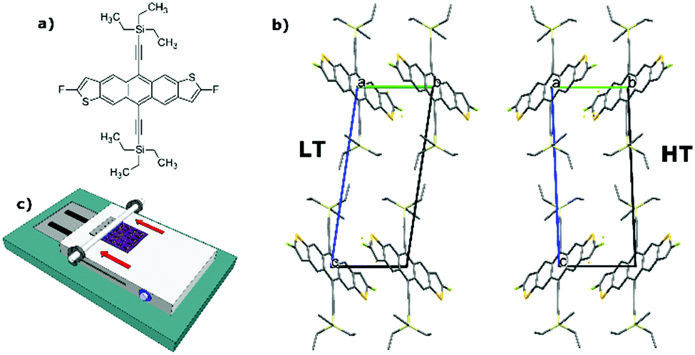 | ||
| Fig. 1 (a) Molecular structure of diF-TES-ADT; (b) comparison of the two unit cells of the HT and LT polymorphs of diF-TES-ADT; (c) schematic representation of the BAMS apparatus. | ||
Due to the outstanding performance of diF-TES-ADT, with mobility values up to 6 cm2 V−1 s−1 in single crystals5 and 20 cm2 V−1 s−1 in thin films with polymeric dielectrics,26,27 combined with its easily processability in common organic solvents, this molecule has been a point of focus in the fabrication of thin-film OFETs by solution-based techniques.28 However, very limited efforts have been devoted to the understanding of its polymorphism scenario, despite the fact that the phase transition occurring near room temperature anticipates that both LT and HT polymorphs could be easily accessible in normal conditions.
Recently, we reported the preparation of crystalline thin films from blends of diF-TES-ADT and polystyrene (PS) by bar-assisted meniscus shearing (BAMS).29 The resulting devices displayed mobilities around 1.5 cm2 V−1 s−1, threshold voltage close to 0 V and on/off current ratio ≈107. Here, we report how by fine tuning the shearing speed of the diF-TES-ADT:PS blend, we were able to control the LT/HT polymorph ratio and check the impact of the phase mixing and of the thin film morphology on the OFET electrical response. Selected shearing conditions allowed for the fabrication of highly oriented films of pure LT polymorph, which gave the possibility to study the strong anisotropy of the charge transport in this system. Importantly, we demonstrate that the two so-called high/low-T polymorphs can be accessed at room temperature by playing with the deposition parameters that influence the kinetics and thermodynamics of the crystallisation process.
2. Experimental
Solutions of diF-TES-ADT (Lumtec, purity >99%, 50/50 mixture of anti and syn isomers) blended with PS of molecular weight 10 kg mol−1 (Sigma-Aldrich) in chlorobenzene (CB, Sigma-Aldrich HPLC grade) were prepared.The solution concentration and diF-TES-ADT:PS ratio were fixed at 2% w/w and 4![[thin space (1/6-em)]](https://www.rsc.org/images/entities/char_2009.gif) :1, respectively.
:1, respectively.
Bottom gate/bottom contact (BGBC) OFETs were fabricated starting from heavily p-doped Si/SiO2 wafers from Si-Mat (SiO2 of thickness 200 nm, C = 17.25 nF cm−2). Interdigitated electrodes of various channel lengths (L = 25, 50, 75 and 100 μm, with W/L 100) were fabricated by photolithography (Micro-Writer ML3 from Durham Magneto Optics Ltd, resolution 5 μm). To check the anisotropy effect on the electrical performances, two orthogonal device orientations were defined.
Before depositing the OSC layer, the gold electrodes were exposed for 25 minutes to ozone for the surface activation and then functionalized with a self-assembled monolayer (SAM) of pentafluorobenzothiol (PFBT, Sigma-Aldrich) by immersion in a 2 μl ml−1 isopropanol solution for 15 min.
All the films were deposited by the previously reported BAMS technique.30 During the deposition, the substrate temperature was kept constant at 105 °C, and the shearing speed was varied between 0.1 and 20 mm s−1.
The thin film morphology was investigated with Olympus BX51 microscope equipped with polarizer and analyzer at 90° in reflection mode for observation in crossed polarizers configuration.
Film topography and thickness were extracted by atomic force microscopy (AFM) images (Keysight 5100 system from Agilent) taken in constant amplitude dynamic mode. The images were analyzed with the Gwyddion 2.52 software.
Film crystallinity and polymorphism was examined with X-ray diffraction (XRD) out-of-plane measurements in θ/2θ configuration (Siemens D-5000 diffractometer) employing Cu-Kα1 radiation (λ = 1.5406 Å) at ambient conditions. The (001) peaks were fitted to a Voigt function, which is a common model for XRD peak analysis.31
The electrical characteristics were assessed under ambient conditions using an Agilent B1500A semiconductor parameter analyzer connected to the sample with a Karl SÜSS probe station. Transfer characteristics were measured in the linear and saturation regimes, with VD fixed at −5 V and −15 V, respectively, while VG was swept between +5 V and −20 V forward and backward. Output characteristics were also measured under constant VG = +5, −5, −15 and −25 V, while VD was swept between +5 V and −25 V, also forward and backward. The mobility and threshold voltage were extracted in the saturation regime. The mobility was calculated using the following equation:
The threshold voltage (Vth) was calculated from the linear fit of |ID|1/2vs. VG at the interception with the x-axis.
3. Results and discussion
Thin films of diF-TES-ADT:PS were deposited by BAMS following the previous reported methodology (Fig. 1c).29 A mixture of 50/50 of anti/syn diF-TES-ADT isomers were employed in these experiments.32 The substrate temperature was always kept at 105 °C during deposition, while the shearing speed applied was 0.1, 1, 10, 15 and 20 mm s−1. In the following, we describe how the coating speed impact on the thin film structure and, in turn, on the OFET device properties.The solution shearing speed is known to determine the crystallization regime.20 At fast shearing rate (typically ≥10 mm s−1) a wet film is formed and then nuclei can grow in all directions while the solvent evaporates. This is the so-called Landau–Levich regime, which leads to thicker films when increasing the coating speed. In contrast, when the bar displaces slowly (i.e., ≤1 mm s−1) the crystallisation follows a convective regime, where the solvent evaporates simultaneously to the solution deposition. Thus, nuclei grow preferentially in one direction, because the material in the backward region is already dry. In this case, the film thickness increases when lowering the speed. For all the sets of devices prepared here, we observed the same tendency of thickness as a function of the shearing speed. Slower shearing speeds produce much thicker films, ranging from less than 30 nm at 10 mm s−1, to 80 nm at 1 mm s−1 and to 160 nm at 0.1 mm s−1. However, above 10 mm s−1 the trend changes and increasing the speed results in an increase of the thickness again, reaching 50 nm at 15 mm s−1 and 60 nm at 20 mm s−1 (Table S1, ESI†). This is in agreement with the two crystallisation mechanisms described above, where at 10 mm s−1 we find the thinnest films and the transition from the convective to the Landau–Levich regime.33 These different crystallisation processes can significantly impact on the thin film morphology and crystal structure. Previously, it was found that at the transition region between the two regimes, higher quality films were formed giving a better OFET performance.20,21
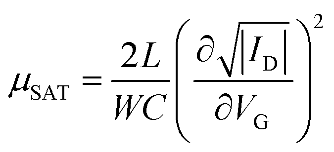
Comparison of optical polarised microscope (POM) images and AFM topography images of diF-TES-ADT:PS thin films are shown in Fig. 2. The film at 10 mm s−1 shows large petal-like crystallites with clear boundaries that can be appreciated in its corresponding AFM topography image. This type of morphology is consistent with previous reports of spin-cast blends of this OSC with PS.34 The grains are smaller in the channel area than on the SiO2 regions far from the electrodes. This can be attributed to higher nucleation density taking place on the PFBT-treated electrodes than on the polar dielectric. It has been previously reported that the F⋯F and F⋯S interactions between the PFBT SAM and the OSC facilitate the nucleation of diF-TES-ADT on the modified source/drain electrodes.35,36
 | ||
| Fig. 2 POM (top panels) and AFM topography (bottom panels) images of the diF-TES-ADT:PS thin film OFETs prepared at different solution shearing speeds. In all these films the shearing directions coincides with the channel length. The scale bars in the AFM images correspond to 10 μm. | ||
At 10 mm s−1 shearing speed, the films are isotropic formed by randomly oriented crystal domains between the source–drain interdigitated contacts (Fig. 2). However, as the speed decreases to 1 and 0.1 mm s−1, the morphologies become distinctly oriented along the shearing direction. Further, in the films fabricated at these lower rates, the electrodes do not appear to play a significant role in the nucleation process. The AFM images of films fabricated at 0.1 and 1 mm s−1 show long plate-like crystal domains (Fig. 2) almost perfectly orientated, separated by more pronounced boundaries at the lower speed. When increasing the thin film deposition speed (i.e., 15 and 20 mm s−1), the film morphology retains the same shape of the randomly oriented crystallites obtained at 10 mm s−1 but with increased crystal domain dimensions.
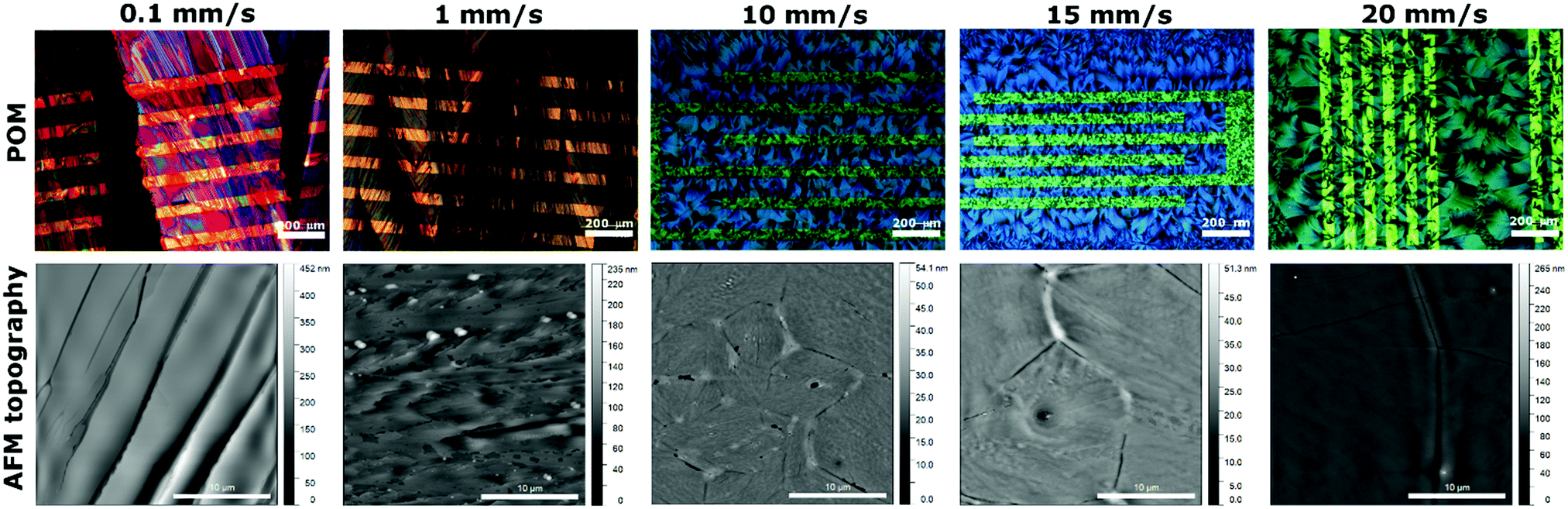
As previously introduced diF-TES-ADT has two enantiotropic polymorphs which have an almost room temperature transition. Therefore, the structural characterisation of the films was pursued in order to establish possible structural differences for the samples fabricated at different shearing speed. The complete experimental XRD spectrum of the sample sheared at 10 mm s−1 is displayed in Fig. S1 (ESI†) alongside the predicted powder patterns of both diF-TES-ADT polymorphs for comparison. Only (00l) reflections are discernible in the XRD indicating that the samples are preferentially oriented with the c axis perpendicular to the substrates. The crystal structure of the samples was analysed through the (001) peak since this is the most intense one, as observed in the film sheared at 10 mm s−1 which is reported in the ESI† (Fig. S2). Despite the XRD is not conclusive for micrometric spatial distribution of the polymorphs, some observations can be realised. All samples prepared with a shearing speed of 10 mm s−1 appear to be composed of phase mixture since the (001) peak unfolds into two contributions: a 2θ peak around 5.39°, compatible with the LT polymorph, and another one appearing at a higher value around 5.45°, in agreement with the HT structure. The heights of the two peaks can be directly comparable because both LT and HT structures have a similar structure factor for the (001) reflection: |F|(001) = 64.2424 for the HT phase and |F|(001) = 63.5043 for the LT phase. The structure factors have been calculated for the Cu-Kα1 wavelength with the VESTA software37 from the structure files published by Jurchescu and coworkers.25
With the aim to investigate how the shearing speed affects the crystallization process of the films, we analysed the (001) peak in all the films since it can be used to discriminate between LT and HT phases, as previously reported.25 According to the reported structures of the two polymorphs, the (001) peak positions for the working wavelength are 2θLT = 5.37° and 2θHT = 5.41°. Considering this, the complete set of XRD diffractograms with the deconvolution analysis, when needed, was realised and is reported in Fig. 3. In cases where a one-peak fit yields a higher R2 than a two-peak fit, the former was chosen.
 | ||
| Fig. 3 (001) peak fits of the films fabricated with diF-TES-ADT:PS at 0.1, 1, 10, 15 and 20 mm s−1. | ||
At the lowest shearing speed only one peak, centred at 5.39°, is observed and attributed to the LT polymorph. Generally speaking, at this lower speed the most thermodynamically stable polymorph should be favoured. At the highest speed (i.e., 20 mm s−1) where the kinetic phase is more favoured, the peak becomes broader and shifts to 5.49° compatible with the formation of the HT polymorph.25 In the intermediate speeds we find a phase mixing of the two polymorphs with different ratios according to the applied velocity. Noticeably, the phase mixture is not distinguished by a different crystal morphology (see Fig. 2). This can be ascribed to the similarity of the two polymorphs, which can hence be coexisting without distorting the film homogeneity. Therefore, we succeed in controlling the formed diF-TES-ADT polymorphs not by heating/cooling the films but instead by modifying the deposition conditions. In this way, both HT and LT phases can be accessed and stabilised at the same ambient conditions.
The effect of the thin films structure on the OFET performance was explored by analysing sets of at least 30 devices for each fabrication condition. Comparison of the electrical performance of samples were assessed using the saturation regime mobility as figure of merit. No clear dependence of the mobility with channel length was observed for all the fabrication conditions. The average mobility of the samples as a function of shearing speed is displayed in Fig. 4a. Devices fabricated at 1 and 0.1 mm s−1 display strong transport anisotropy, as it will be discussed later. For these samples, only data from devices with the channel parallel to the shearing direction are included in the plot, as their mobility are remarkably higher than those perpendicularly oriented (see below for further discussion).
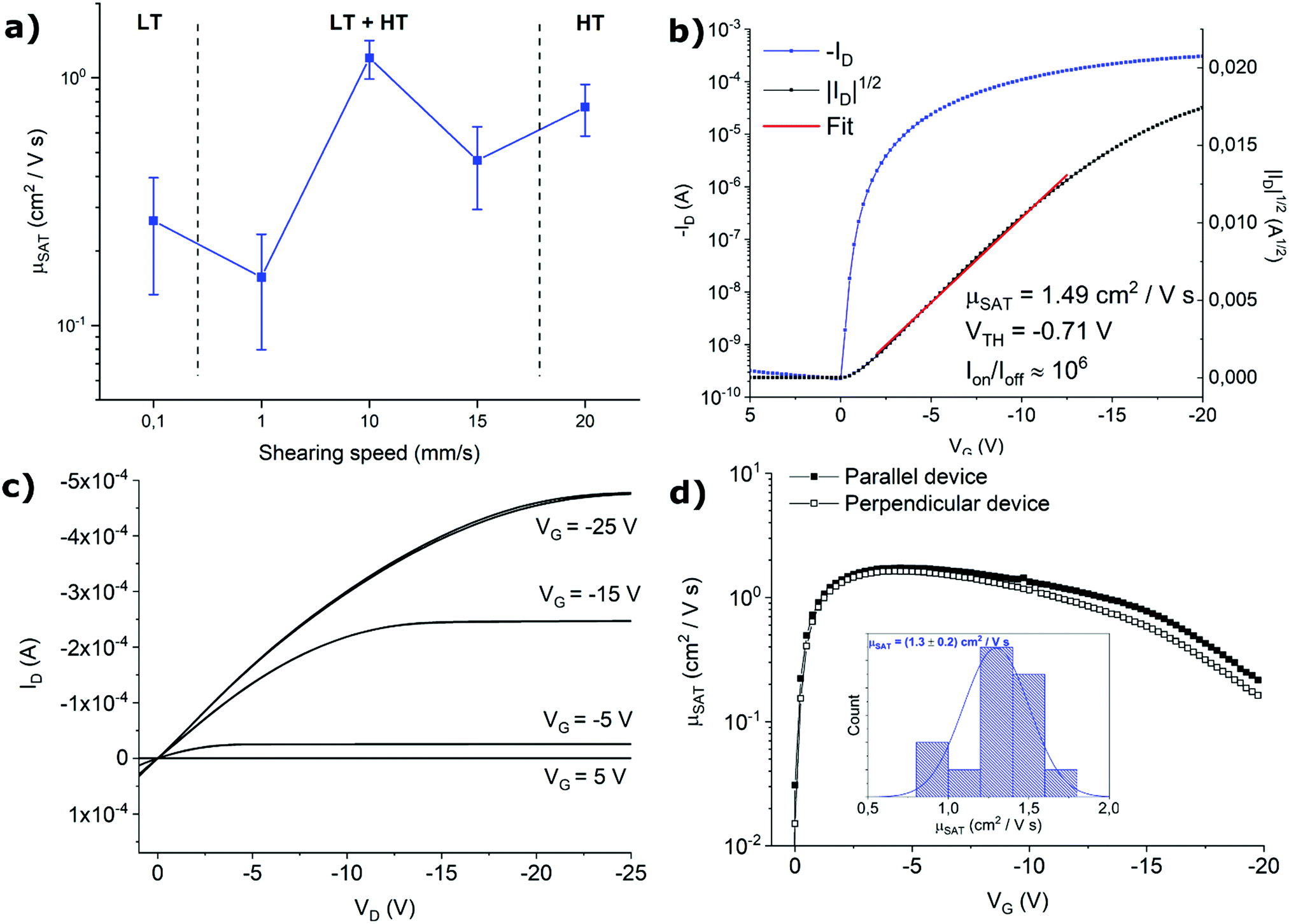 | ||
| Fig. 4 (a) Mobility vs. shearing speed plot. Representative transfer (b) and output (c) characteristics for a diF-TES-ADT:PS film deposited at 10 mm s−1. (d) Mobility profiles for films coated with the channel parallel (filled squares) and perpendicular (empty squares) to the shearing direction (inset: device mobility statistics). | ||
Previously, it was reported that the HT polymorph exhibited a greater OFET mobility than the LT polymorph.25 Accordingly, here we found that at lower shearing speeds of 0.1 and 1 mm s−1, where the films are based or enriched with the LT polymorph, a lower mobility is found around 0.1–0.3 cm2 V−1 s−1. Contrary, in the other extreme, the films based on only or with a larger proportion of the HT polymorph prepared at high coating speeds of 20 and 15 mm s−1, respectively, the mobility is increased to 0.5–0.8 cm2 V−1 s−1. Remarkably, the best performance is found in the devices prepared at 10 mm s−1, that is in the transition between the two crystallisation regimes. At this point, a phase mixture is clearly present in the films. These results were unexpected since phase mixing has typically a detrimental effect on the devices performances due to the stress occurring in the grain boundaries.38,39 We believe that here there is an interplay between morphological and structural effects taking place. As mentioned, typically the films prepared in the transition area between the two crystallisation regimes are thinner and exhibit a higher device performance. Here, this effect might be the dominant one considering that the two polymorphs are very similar and can hence coexist without hampering excessively the device mobility.
In Fig. 4b and c representative transfer and output characteristics curves for the films prepared at 10 mm s−1 are reported. The samples processed with this condition reveal a high performance with an average μSAT of 1.3 cm2 V−1 s−1 and a VTH close to zero, showing close-to-ideal performance, with a very sharp switch-on, leading to efficient operation. The devices showed little device-to-device variation (Fig. 4d inset) and negligible anisotropy. The mobility profile versus VG shows a relatively low voltage dependence for devices both oriented parallel and perpendicular to the shearing direction, especially in the range VG = −2 − (−10) V (Fig. 4d).
As mentioned above, samples fabricated at 1 and 0.1 mm s−1 display strong anisotropy in charge transport. To illustrate this result, representative transfer curves of devices with orthogonal orientations with respect to the solution shearing direction fabricated at 1 mm s−1 are presented in Fig. 5 (Fig. S3 (ESI†), shows the devices fabricated at 0.1 mm s−1). From the output characteristics it can be observed that all the parallel-oriented devices exhibit more contact resistance than perpendicular-oriented ones, as indicated by the shape of the output curves at low VD (Fig. S4, ESI†). The transport anisotropy is evidenced by the different mobility extracted. Parallel devices exhibit a mobility 4 times larger than perpendicular ones. The perpendicular devices show VTH shifted to more negative values, which can be an indication of more interfacial charge traps. The electrical anisotropy found can be easily rationalized in terms of thin film morphology since, as observed in the POM images, the thin films prepared at low shearing speed exhibit oriented crystalline stripe-like domains grown along the molecular π–π stacking direction. Additionally, in these samples, deep grain boundaries perpendicular to the channel conduction direction are present, which are detrimental to charge transport. Future work will be devoted to understanding the crystallographic directions present in the films.
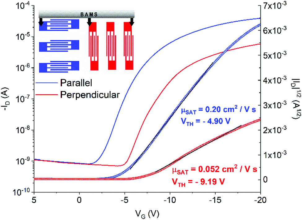 | ||
| Fig. 5 Transfer characteristics of representative OFET devices with channel length parallel (blue line) and perpendicular (red line) with respect to the solution shearing direction, fabricated at 1 mm s−1. | ||
4. Conclusions
In summary, we demonstrated that by tuning the solution shearing speed during the deposition of a blend solution of diF-TES-ADT:PS, the morphology and structure of the films can be tuned. Importantly, it has been found that the polymorphic composition of the so-known HT and LT phases of the OSC can be modulated. At low speed (i.e., at 0.1 mm s−1) the pure LT phase is obtained, while at the highest speed the HT phase is formed. The intermediate speeds lead to a phase mixture.Regarding the OFET performance, the devices in which the LT polymorph predominates exhibit lower mobility than the ones with HT-polymorph, in agreement with previous studies. Surprisingly though, the best performances are found in devices with a mixture of the two polymorphs which were coated at the intermediate shearing speed of 10 mm s−1. These OFETs exhibit isotropic electrical characteristics with a mobility above 1 cm2 V−1 s−1 and a threshold voltage close to 0. This has been attributed to the balance of the morphological and structural effects that are playing a role. Even though phase mixture is generally detrimental for the transport characteristics, this effect might be moderate here due to the similarity of the two diF-TES-ADT polymorphs. On the other hand, the thinner and better quality films formed in the transition region of the two crystallisation regimes, might be responsible for the enhanced OFET performance found.
In conclusion, we demonstrate that modifying the deposition speed in solution sheared films is a very useful tool to control polymorphism. The identification of polymorphism in thin films of OSCs can be quite complex, however, understanding this phenomenon is crucial to realise highly reproducible devices. This is clearly the case of the benchmark diF-TES-ADT semiconductor, since it shows two enantiotropic polymorphs close to room temperature. Therefore, special attention should be paid to control polymorphism in this particular, and widely employed, organic semiconductor.
Conflicts of interest
There are no conflicts to declare.Acknowledgements
This work was funded by the DGI (Spain) project FANCY CTQ2016-80030-R and GENESIS PID2019-111682RB-I00, the Generalitat de Catalunya (2017-SGR-918) and the Spanish Ministry of Economy and Competitiveness, through the “Severo Ochoa” program for Centers of Excellence in R&D (SEV-2015-0496). T. S. acknowledges the H2020-MSCA-COFUND-2014 Programme (P-SPHERE, Grant agreement 665919). We acknowledge support of the publication fee by the CSIC Open Access Publication Support Initiative through its Unit of Information Resources for Research (URICI).References
- M. M. Torrent and C. Rovira, Chem. Soc. Rev., 2008, 37, 827–838 RSC.
- H. Bronstein, C. B. Nielsen, B. C. Schroeder and I. McCulloch, Nat. Rev. Chem., 2020, 4, 66–77 CrossRef CAS.
- O. D. Jurchescu, J. Baas and T. T. M. Palstra, Appl. Phys. Lett., 2004, 84, 3061–3063 CrossRef CAS.
- V. Podzorov, S. E. Sysoev, E. Loginova, V. M. Pudalov and M. E. Gershenson, Appl. Phys. Lett., 2003, 83, 3504–3506 CrossRef CAS.
- O. D. Jurchescu, S. Subramanian, R. J. Kline, S. D. Hudson, J. E. Anthony, T. N. Jackson and D. J. Gundlach, Chem. Mater., 2008, 20, 6733–6737 CrossRef CAS.
- R. J. Kline, S. D. Hudson, X. Zhang, D. J. Gundlach, A. J. Moad, O. D. Jurchescu, T. N. Jackson, S. Subramanian, J. E. Anthony, M. F. Toney and L. J. Richter, Chem. Mater., 2011, 23, 1194–1203 CrossRef CAS.
- M. J. Kang, E. Miyazaki, I. Osaka, K. Takimiya and A. Nakao, ACS Appl. Mater. Interfaces, 2013, 5, 2331–2336 CrossRef CAS.
- H. Ebata, T. Izawa, E. Miyazaki, K. Takimiya, M. Ikeda, H. Kuwabara and T. Yui, J. Am. Chem. Soc., 2007, 129, 15732–15733 CrossRef CAS.
- K. Nakayama, Y. Hirose, J. Soeda, M. Yoshizumi, T. Uemura, M. Uno, W. Li, M. J. Kang, M. Yamagishi, Y. Okada, E. Miyazaki, Y. Nakazawa, A. Nakao, K. Takimiya and J. Takeya, Adv. Mater., 2011, 23, 1626–1629 CrossRef CAS.
- Z. A. Lamport, H. F. Haneef, S. Anand, M. Waldrip and O. D. Jurchescu, J. Appl. Phys., 2018, 124, 071101 CrossRef.
- Y. Diao, B. C. K. Tee, G. Giri, J. Xu, D. H. Kim, H. A. Becerril, R. M. Stoltenberg, T. H. Lee, G. Xue, S. C. B. Mannsfeld and Z. Bao, Nat. Mater., 2013, 12, 665–671 CrossRef CAS.
- Y. Diao, K. M. Lenn, W. Y. Lee, M. A. Blood-Forsythe, J. Xu, Y. Mao, Y. Kim, J. A. Reinspach, S. Park, A. Aspuru-Guzik, G. Xue, P. Clancy, Z. Bao and S. C. B. Mannsfeld, J. Am. Chem. Soc., 2014, 136, 17046–17057 CrossRef CAS.
- A. Rivalta, A. Giunchi, L. Pandolfi, T. Salzillo, S. D’agostino, O. Werzer, B. Schrode, N. Demitri, M. Mas-Torrent, A. Brillante, R. G. D. Valle and E. Venuti, Dyes Pigm., 2020, 172, 107847 CrossRef.
- M. R. Niazi, R. Li, E. Qiang Li, A. R. Kirmani, M. Abdelsamie, Q. Wang, W. Pan, M. M. Payne, J. E. Anthony, D. M. Smilgies, S. T. Thoroddsen, E. P. Giannelis and A. Amassian, Nat. Commun., 2015, 6, 8598 CrossRef CAS.
- S. Riera-Galindo, F. Leonardi, R. Pfattner and M. Mas-Torrent, Adv. Mater. Technol., 2019, 4, 1900104 CrossRef CAS.
- T. Salzillo, A. Campos and M. Mas-Torrent, J. Mater. Chem. C, 2019, 7, 10257–10263 RSC.
- D. Gentili, M. Gazzano, M. Melucci, D. Jones and M. Cavallini, Chem. Soc. Rev., 2019, 48, 2502–2517 RSC.
- H. Chung and Y. Diao, J. Mater. Chem. C, 2016, 4, 3915–3933 RSC.
- S. Riera-Galindo, A. Tamayo and M. Mas-Torrent, ACS Omega, 2018, 3, 2329–2339 CrossRef CAS.
- S. Galindo, A. Tamayo, F. Leonardi and M. Mas-Torrent, Adv. Funct. Mater., 2017, 27, 1700526 CrossRef.
- A. Tamayo, S. Riera-Galindo, A. O. F. Jones, R. Resel and M. Mas-Torrent, Adv. Mater. Interfaces, 2019, 6, 1900950 CrossRef CAS.
- G. Giri, R. Li, D. M. Smilgies, E. Q. Li, Y. Diao, K. M. Lenn, M. Chiu, D. W. Lin, R. Allen, J. Reinspach, S. C. B. Mannsfeld, S. T. Thoroddsen, P. Clancy, Z. Bao and A. Amassian, Nat. Commun., 2014, 5, 3573 CrossRef CAS.
- J. Chen, M. Shao, K. Xiao, A. J. Rondinone, Y. L. Loo, P. R. C. Kent, B. G. Sumpter, D. Li, J. K. Keum, P. J. Diemer, J. E. Anthony, O. D. Jurchescu and J. Huang, Nanoscale, 2014, 6, 449–456 RSC.
- H. Iino, T. Usui and J. I. Hanna, Nat. Commun., 2015, 6, 6828 CrossRef CAS.
- O. D. Jurchescu, D. A. Mourey, S. Subramanian, S. R. Parkin, B. M. Vogel, J. E. Anthony, T. N. Jackson and D. J. Gundlach, Phys. Rev. B: Condens. Matter Mater. Phys., 2009, 80, 085201 CrossRef.
- Z. A. Lamport, K. J. Barth, H. Lee, E. Gann, S. Engmann, H. Chen, M. Guthold, I. McCulloch, J. E. Anthony, L. J. Richter, D. M. DeLongchamp and O. D. Jurchescu, Nat. Commun., 2018, 5130 CrossRef.
- J. Panidi, A. F. Paterson, D. Khim, Z. Fei, Y. Han, L. Tsetseris, G. Vourlias, P. A. Patsalas, M. Heeney and T. D. Anthopoulos, Adv. Sci., 2018, 5, 1700290 CrossRef.
- Q. Zhang, F. Leonardi, S. Casalini, I. Temiño and M. Mas-Torrent, Sci. Rep., 2016, 6, 39623 CrossRef CAS.
- I. Temiño, F. G. Del Pozo, M. R. Ajayakumar, S. Galindo, J. Puigdollers and M. Mas-Torrent, Adv. Mater. Technol., 2016, 1, 1600090 CrossRef.
- F. G. Del Pozo, S. Fabiano, R. Pfattner, S. Georgakopoulos, S. Galindo, X. Liu, S. Braun, M. Fahlman, J. Veciana, C. Rovira, X. Crispin, M. Berggren and M. Mas-Torrent, Adv. Funct. Mater., 2016, 26, 2379–2386 CrossRef CAS.
- T. H. de Keijser, J. I. Langford, E. J. Mittemeijer and A. B. P. Vogels, J. Appl. Crystallogr., 1982, 15, 308–314 CrossRef CAS.
- C. W. Huang, X. You, P. J. Diemer, A. J. Petty, J. E. Anthony, O. D. Jurchescu and J. M. Atkin, Commun. Chem., 2019, 22, 2 Search PubMed.
- D. Grosso, J. Mater. Chem., 2011, 21, 17033–17038 RSC.
- A. B. Naden, J. Loos and D. A. Maclaren, J. Mater. Chem. C, 2014, 2, 245–255 RSC.
- J. W. Ward, M. A. Loth, R. J. Kline, M. Coll, C. Ocal, J. E. Anthony and O. D. Jurchescu, J. Mater. Chem., 2012, 22, 19047–19053 RSC.
- D. J. Gundlach, J. E. Royer, S. K. Park, S. Subramanian, O. D. Jurchescu, B. H. Hamadani, A. J. Moad, R. J. Kline, L. C. Teague, O. Kirillov, C. A. Richter, J. G. Kushmerick, L. J. Richter, S. R. Parkin, T. N. Jackson and J. E. Anthony, Nat. Mater., 2008, 7, 216–221 CrossRef CAS.
- K. Momma and F. Izumi, J. Appl. Crystallogr., 2011, 44, 1272–1276 CrossRef CAS.
- L. L. Chua, J. Zaumseil, J. F. Chang, E. C. W. Ou, P. K. H. Ho, H. Sirringhaus and R. H. Friend, Nature, 2005, 434, 194–199 CrossRef CAS.
- A. L. Briseno, S. C. B. Mannsfeld, M. M. Ling, S. Liu, R. J. Tseng, C. Reese, M. E. Roberts, Y. Yang, F. Wudl and Z. Bao, Nature, 2006, 444, 913–917 CrossRef CAS.
Footnotes |
| † Electronic supplementary information (ESI) available: Additional characterisation information. See DOI: 10.1039/d0tc03222k |
| ‡ T. S. and N. M. equally contributed to this work. |
| This journal is © The Royal Society of Chemistry 2020 |