
 Open Access Article
 This Open Access Article is licensed under a Creative Commons Attribution-Non Commercial 3.0 Unported Licence
Impact of p-type doping on charge transport in blade-coated small-molecule:polymer blend transistors†
Aniruddha
Basu
 *a,
Muhammad Rizwan
Niazi
a,
Alberto D.
Scaccabarozzi
a,
Hendrik
Faber
a,
Zuping
Fei
b,
Dalaver H
Anjum
c,
Alexandra F.
Paterson
a,
Olga
Boltalina
d,
Martin
Heeney
e and
Thomas D.
Anthopoulos
*a
*a,
Muhammad Rizwan
Niazi
a,
Alberto D.
Scaccabarozzi
a,
Hendrik
Faber
a,
Zuping
Fei
b,
Dalaver H
Anjum
c,
Alexandra F.
Paterson
a,
Olga
Boltalina
d,
Martin
Heeney
e and
Thomas D.
Anthopoulos
*a
aKing Abdullah University of Science and Technology (KAUST), KAUST Solar Center (KSC), Thuwal 23955-6900, Kingdom of Saudi Arabia. E-mail: thomas.anthopoulos@kaust.edu.sa; aniruddha.basu@kaust.edu.sa
bInstitute of Molecular Plus, Tianjin Key Laboratory of Molecular Optoelectronic Science, Tianjin University, Tianjin, 300072, P. R. China
cKAUST CoreLabs, King Abdullah University of Science and Technology, Thuwal 23955-6900, Kingdom of Saudi Arabia
dDepartment of Chemistry, Colorado State University, Fort Collins, CO 80523, USA
eDepartment of Chemistry and Centre for Plastic Electronics, Imperial College London, South Kensington, London SW7 2AZ, UK
First published on 3rd September 2020
Abstract
Blade-coating is a roll-to-roll (R2R) compatible processing technique and has the potential to address the industry's needs for scalable manufacturing of future organic electronics. Here we investigate the applicability of blade-coating for the fabrication of organic thin-film transistors (OTFTs) based on best-in-class organic semiconducting blends comprised of the conjugated small-molecule 2,7-dioctyl[1]benzothieno[3,2-b][1]benzothiophene (C8-BTBT), and the conjugated polymer poly(indacenodithiophene-co-benzothiadiazole) (C16IDT-BT). We show that the operating characteristics of blade-coated transistors consistently outperform devices prepared via spin-coating, showcasing the compatibility of the technique. Introducing the molecular p-dopant C60F48 into the binary C8-BTBT:C16IDT-BT blend formulation, in combination with carefully optimized blade-coating conditions, helps to enhance the performance of the ensuing transistors further resulting in a maximum hole mobility of ≈14 cm2 V−1 s−1, and an all-around improvement of the device operating characteristics. Our results show that p-doped blend OTFTs can be manufactured using industry relevant processing techniques without sacrificing their state-of-the-art performance.
1. Introduction
The vast majority of modern day electronics rely on inorganic materials that require complex and costly manufacturing processes.1,2 Emerging semiconductor technologies such as organic semiconductors (OSCs) promise to provide an alternative option for implementation in various future opto-electronics including flexible, foldable, wearable, stretchable and even disposable devices for application in health, security, information, display, sensing and energy generation, among many others.3–8 This has resulted in continuous exploration of OSCs as active layers in printable organic photovoltaics (OPVs), organic light emitting diodes (OLEDs), thermoelectrics, and organic thin-film transistors (OTFTs).3,6,9–12Among the various demonstrated technologies, OTFTs are highly promising as the building blocks for large-area electronics and more broadly for the internet of things (IoT) device ecosystem.13,14 During the past three decades, continuous progress on materials development, interfaces and device engineering have resulted in field-effect mobility (μ), a key figure of merit, of >20 cm2 V−1 s−1.5,15–18 Laboratory-based research often relies on the widely available film deposition method of spin-coating. Unfortunately, the latter is wasteful (90–95% material waste) and incompatible with continuous, high-throughput roll-to-roll (R2R) printing techniques relevant to manufacturing of the envisaged electronics of the future. To this end, meniscus guided R2R compatible techniques such as blade, knife, bar and slot-die coating, are more relevant to the industry offering 95–99% utilization of the OSC ink.5,9,10,19–23 The drying kinetics during solution-phase deposition is known to strongly influence the morphology, crystallinity and microstructure of the resulting layers, ultimately dictating the charge transport properties of the formed OSC films and their devices.5,23–28 Though meniscus guided techniques have been used in the past to deposit OSC films with aim to understand the structure–property–performance relationship for OTFTs,27,29–34 the majority of these studies relied on low to medium coating speeds.27
In recent years, molecular doping of OSCs has emerged as promising method to enhance the performance of solution-processed OTFTs.18,35–48 In this regard, we have recently developed p-doped OTFTs with hole mobility of 13 cm2 V−1 s−1 based on spin-coated blend semiconducting channels based on the small-molecule 2,7-dioctyl[1]benzothieno [3,2-b][1]benzothiophene (C8-BTBT), and the polymer poly(indacenodithiophene-co-benzothiadiazole) (C16IDT-BT).16 Key to our success has been the ink-formulation engineering (solvents, material ratios, etc.), in combination with careful choice of drying kinetics (spin-coating and melt-processing conditions). Using this work as our starting point, we attempt to bridge the existing gap between lab-scale and industry relevant manufacturing of high-performance blend OSCs and their use in OTFTs. We first studied the role of coating method (spin vs. blade coating) on the morphology and charge transport of the blend OSCs and their OTFTs. We find that blade-coated devices consistently outperform their spin-coated counterparts, an observation attributed to the superior morphology of blade-coated layers due to different film formation conditions. By introducing the molecular p-dopant C60F48 into the C8-BTBT:C16IDT-BT blend and blade-coating it at industry relevant speeds of >1 m min−1, we are able to improve the mobility of the OTFTs further reaching a maximum value of 14 cm2 V−1 s−1. The work highlights the compatibility of high performance blend OSCs with the industry-relevant blade-coating technique while providing important guideline for the processing of high quality blend OSC and the realization of state-of-the-art OTFTs.
2. Result and discussion
The molecular structures and corresponding energy levels of C8-BTBT, C16IDT-BT and the p-dopant (C60F48) are shown in Fig. 1a and b, respectively, while Fig. 1c depicts the blade-coating process. Further details on the blade-coating process and the relevant parameters are given in Fig. S1 in the ESI.† Blade-coating involves two main coating regimes: (1) the evaporation regime, and (2) the Landau–Levich (L–L) regime, which depend primarily on the coating speed.25,49,50 For the purpose of this work we optimized and set the coating speed at 50 mm s−1 (3 m min−1) while maintaining the stage temperature at 70 °C. The latter falls within the L–L coating regime (>20 mm s−1) and it is representative of industrial roll-to-roll solution printing requirements.23 Unlike spin-coating, blade-coating is a meniscus guided coating technique which can help to control the nucleation, crystal growth and orientation of the small molecule (SM) films over a large coating area.51 Blade-coating and spin-coating of all blend layers investigated was performed entirely under inert nitrogen atmosphere in order to eliminate extrinsic effects such as unintentional doping, variable humidity conditions etc.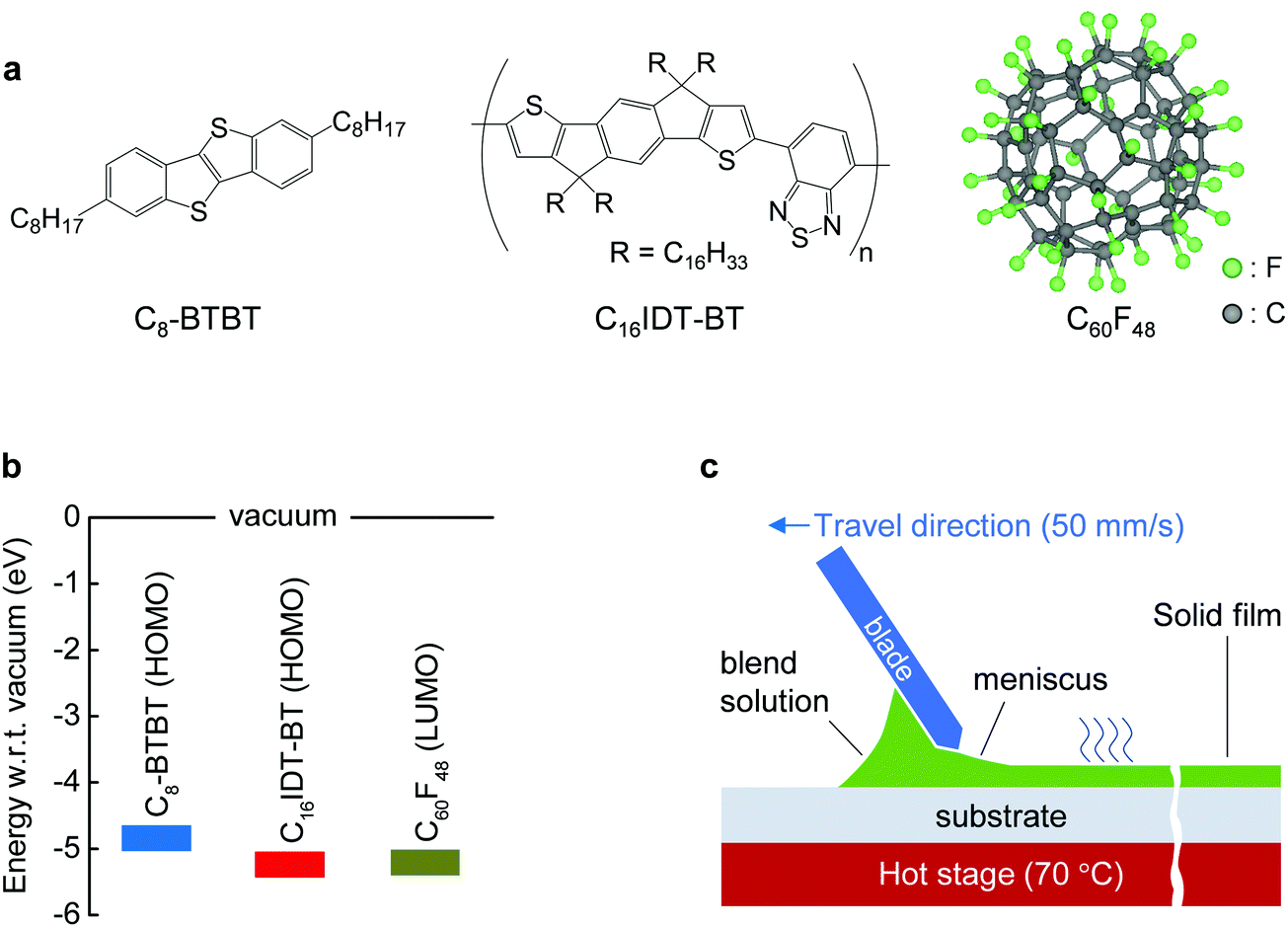 | ||
| Fig. 1 (a) Chemical structures of C8-BTBT, C16IDT-BT and C60F48 used in this study. (b) Highest occupied molecular orbital (HOMO) energy levels of C8-BTBT and C16IDT-BT, and lowest unoccupied molecular orbital (LUMO) energy level of C60F48. (c) Schematic depicting the blade-coating process and the various parameters used. | ||
We employed polarized optical microscopy (POM), atomic force microscopy (AFM), cross sectional transmission electron microscopy (TEM), and grazing incidence wide angle scattering (GIWAXS) techniques to assess the morphology, vertical phase separation and microstructure of the thin films coated by two coating methods. POM micrographs of blade and spin-cast pristine blend films (Fig. 2a and b) reveal that blade-cast films are characterized by small nucleation density and larger poly-crystalline domains. The differences are attributed to the different crystallization/phase-transformation mechanisms involved in the two coating techniques.23
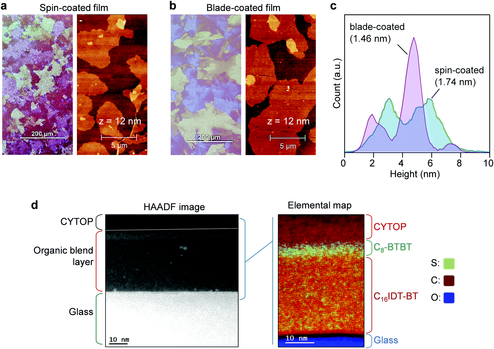 | ||
| Fig. 2 (a and b) Polarized optical microscopy and atomic force microscopy images of spin-coated and blade-coated C8-BTBT:C16IDT-BT blend layers. (c) Surface height distribution profiles extracted from the AFM images of the spin-coated and blade-coated blend films. (d) X-TEM analysis of the C8-BTBT:C16IDT-BT blend film deposited on glass. The image on the left is the HAADF-STEM image while the one on the right shows an RGB Composite of S, C, and O maps generated by processing the STEM-EELS data-cubes. | ||
AFM analysis of the layers’ surfaces reveal the presence of molecular terraces of C8-BTBT on both spin and blade cast blend films, in agreement with previous reports.16,17 The height histograms (Fig. 2c) extracted from 20 × 20 μm2 AFM scans, reveal that the majority of the molecular plateaus in blade-coated films have a height in the range 4–5.40 nm (peak at ≈4.7 nm) and a smaller fraction of plateaus with heights in the range 1.40–2.70 nm (peak at ≈1.9 nm). Similarly, the height distribution for the spin-coated films also exhibit two main peaks, one between 2.40–3.64 nm (peak at ≈3.1 nm) and a second one between 4.8–6.3 nm (peak at ≈5.75 nm). These differences manifest in a lower root mean square (RMS) surface roughness of 1.46 nm for the blade-coated layers as compared to 1.74 nm for the spin-coated films. The blade-cast films exhibit larger polycrystalline domains, in line with POM images, suggesting a higher film quality than the spin-cast layers. The characteristic height distributions seen in both films is most likely the result of the presence of domains (crystallites) composed of different number of monomolecular layers of the C8-BTBT lamella, while the broadening of these peaks is most likely the result of the non-uniform nature of the vertical phase-separated system. To this end, a monomolecular terrace step height of ≈2.8 nm should be expected for the c-axis of C8-BTBT, which should dominate in films with an out-of-plane molecular packing motif. The measured surface heights are those in broad agreement with the presence of large monomolecular domains.
Lastly, we investigated the vertical phase separation in the blend layers using transmission electron microscopy (TEM) in conjunction electron energy loss spectroscopy (EELS) mode. The vertical phase separation in small-molecule:polymer blend systems is believed to proceed via the nucleation and growth of the small-molecule component.16,17,52 In particular, the as-deposited wet layer first undergoes a liquid–liquid phase separation (driven by the surface energies of the different blend components) before the small-molecule (i.e. C8-BTBT here) starts to crystallize. This crystallization even becomes particularly pronounced at the surface/air interface of the supersaturated solution, leading to the formation of the small-molecule dominated layer surface. The remaining part of the layer eventually dries up to form the polymer-dominated phase at the bottom interface (substrate/film) of the composite film. Indeed, the Sulphur map of the blend films shown in Fig. 2d, confirms the AFM observations that the surface of the blend layer is dominated by the presence of C8-BTBT molecules that form a stratified layer approximately ≈7 nm in thickness.
To understand the impact of morphology on charge transport properties, we have fabricated top-gate bottom-contact (TG-BC) OTFTs based on spin-coated blade-coated channel layers of undoped C8-BTBT:C16IDT-BT blends using identical ink-formulation protocols to those reported previously.16,17,53 The ensuing devices were electrically characterized under nitrogen atmosphere at room temperature in order to avoid extrinsic effects such as unintentional doping or degradation due to the presence of oxygen, or other atmospheric oxidants etc. The representative transfer and output curves, measured in linear and saturation biasing regimes, are shown in Fig. 3a and Fig. S2 (ESI†). The average saturation mobility (μSAT) for spin-cast devices was found to be 2.4 (±0.7) cm2 V−1 s−1, in excellent agreement to our earlier published reports.16,17 Details of the method used to calculate μSAT are provided in the Experimental section of the manuscript. On the other hand, TGBC devices based on blade-cast films yielded a significantly higher μSAT value of 6 cm2 V−1 s−1. Fig. S3 (ESI†) shows the statistical comparison of the device performance of spin-coated and blade-coated OTFTs. The measured current–voltage (I–V) characteristics are hysteresis free which is indicative of a high quality semiconductor/dielectric interface.
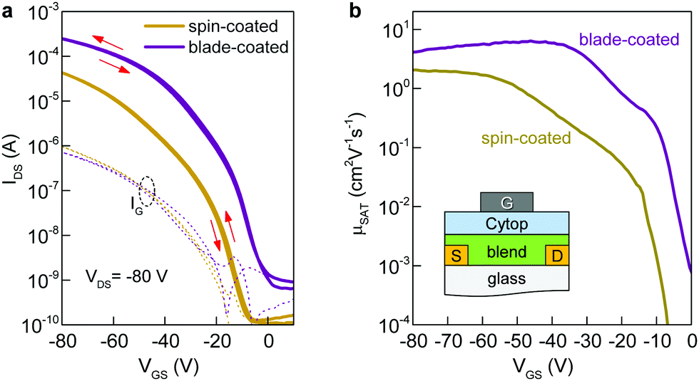 | ||
| Fig. 3 (a) Transfer characteristics of spin-coated and blade-coated C8-BTBT:C16IDT-BT OTFTs measured at VDS = −80 V. Dotted lines represents the corresponding gate leakage (IG) currents. The channel width and length of the devices were 1000 μm and 80 μm, respectively. (b) Hole mobility measured in saturation (μSAT) versus applied gate bias (VGS) for the C8-BTBT:C16IDT-BT-based OTFTs shown in (a). | ||
We also assessed the reliability of the calculated μSAT values by examining the mobility dependence on VGS (Fig. 3b) at VDS = −80 V for both spin- and blade-coated devices. OTFTs prepared via spin-coating exhibit a plateau in μSAT at high VGS range while for blade-coated transistors the mobility peaks (6.4 cm2 V−1 s−1) at lower VGS followed by a reduction (4.1 cm2 V−1 s−1) at higher voltages. This is a known phenomenon in OTFTs and has been previously associated with the presence of contact resistance that is also affected by the applied gate-field.54 To avoid overestimation, we thus use the mobility values calculated at VGS = −80 V as the representative parameter for both spin-cast and blade-coated transistors. The improved μSAT for blade-coated devices manifests as larger channel on-currents (a factor of six) and lowered VTH as compared to spin-coated transistors (Table S1, ESI†). The noticeable differences in the charge transport between spin-coated and blade-coated OTFTs are almost certainly attributed to morphology and microstructure differences of the channel layer.55–57 Importantly, both types of OTFTs show good shelf lifetime with their initial operating parameters being retained for up to six months of storage in a nitrogen atmosphere.
2.1. Effect of molecular p-type doping
We have previously shown that addition of C60F48 in spin-coated C8-BTBT:C16IDT-BT blend channels increases the hole mobility of the OTFTs to 13 cm2 V−1 s−1.16 Motivated by this early work, we deposited pristine and C60F48-doped C8-BTBT:C16IDT-BT layers via blade-coating. Kelvin probe (KP) measurements performed on both types of blend layers (Fig. S4, ESI†) reveal a significant shift in work function (WF) from 4.8 eV, for the pristine blend, to 5.3 eV upon addition of 4.5 mol% C60F48. These results provide direct evidence of successful p-doping of the C8-BTBT:C16IDT-BT blend by C60F48.Next we studied the morphology and microstructure of the blade-coated layers using POM, AFM and GIWAXS. The POM and AFM images shown in Fig. 4a and b reveal the presence of large crystalline domains and molecular terraces due to the vertical phase separation of C8-BTBT at the surface of the blend film. C60F48-doped film exhibit larger C8-BTBT crystalline domains/terraces than the pristine layer. The height distribution profile shown in Fig. 4c supports this conclusion since the surface exhibits a single dominant peak at ≈5.5 nm, which equates to approximately two monomolecular layers of C8-BTBT. The pristine layer on the other hand shows a bimodal distribution of terrace heights, one at 1.9 nm (single monomolecular terrace) and a stronger one at 4.8 nm (double monomolecular terrace), supporting the existence of smaller area terraces/crystals with different heights. As a result of these features the RMS surface roughness of pristine and C60F48-doped blend layers are similar and equal to 1.46 and 1.48 nm, respectively. Fig. S5a (ESI†) shows the AFM images of the blend films doped with several different C60F48 concentrations (i.e. 0.1%, 2% and 4.25%), while Fig. S5b–d (ESI†) show the evolution of the surface height distribution and surface roughness RMS for blend layers with different dopant concentrations, respectively. AFM images with 20 × 20 μm2 scan area were used to extract the height distribution and RMS roughness data. Evidently, the presence of C60F48, at optimal dopant concentration, enables the formation of blend films with more uniform molecular traces (more compact films) and lower RMS surface roughness.
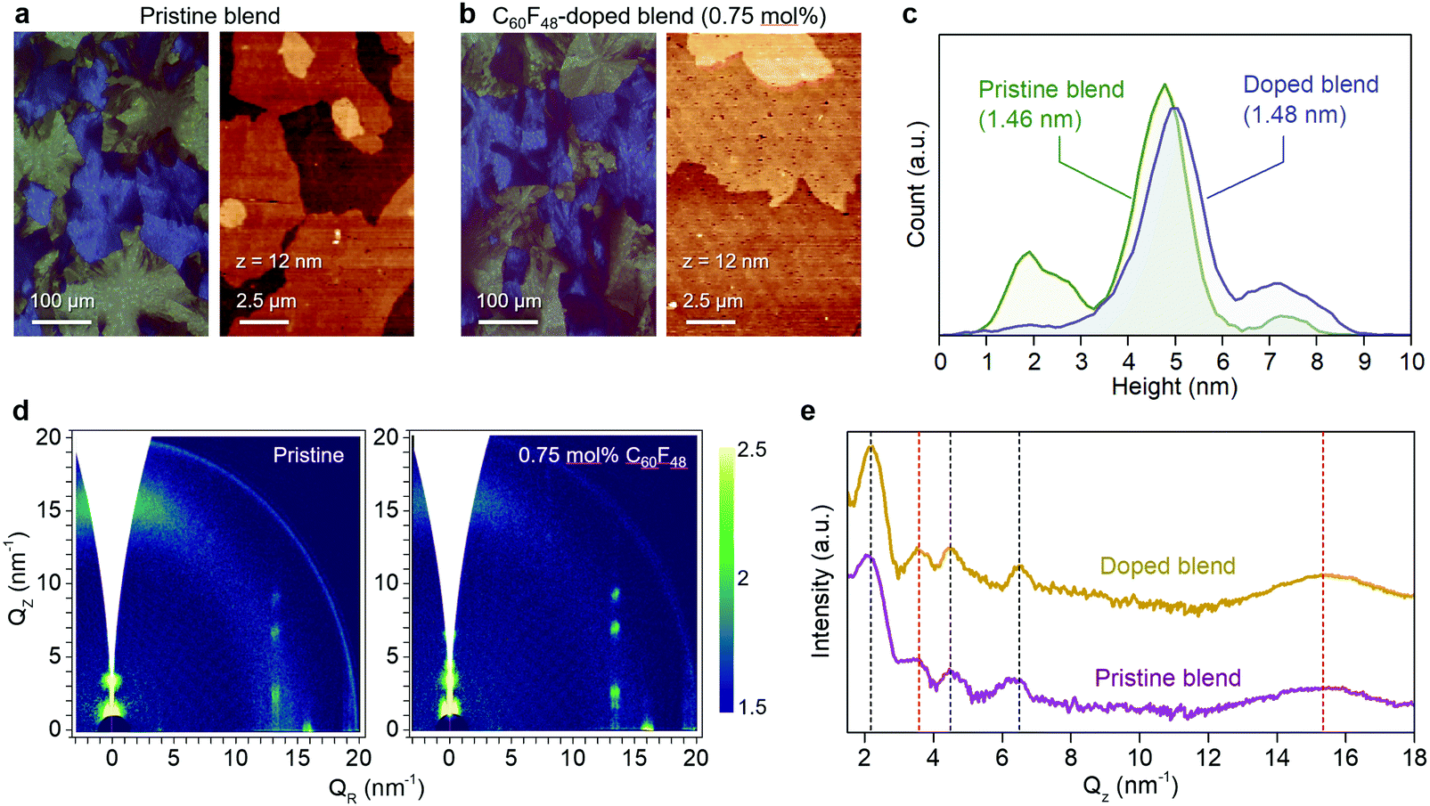 | ||
| Fig. 4 (a and b) Polarized optical microscopy and atomic force microscopy images of pristine and p-doped C8-BTBT:C16IDT-BT layers processed via blade-coating. (c) Surface height histograms of the pristine and p-doped C8-BTBT:C16IDT-BT layers extracted from the AFM images. (d) 2D GIWAXS images of the pristine and p-doped blend layers. (e) Plots of the integrated intensity versus Q (nm−1) for out-of-plane Bragg sheets taken from (d). | ||
Further insights into the microstructure of the blend layers and the role of C60F48 were obtained via two-dimensional GIWAXS (2D GIWAXS) measurements. Fig. 4d shows the 2D GIWAXS images taken for a pristine and a C60F48-doped (0.75 mol%) blade-coated C8-BTBT:C16IDT-BT blend films. The crystal lattice of the doped layer appears similar to that of the pristine, in agreement with previous reports on the effect of doping on spin-coated films.58 In particular, the 2D GIWAXS patterns show a diffraction in the out-of-plane direction (Fig. 4e) at Qz = 3.6 nm−1 where the broad feature at 15 nm−1 is associated to C16IDT-BT (red dotted line), while the other highly oriented and sharp diffractions are related to C8-BTBT (black dotted line). The integrated intensity vs. Qz (nm−1) plots for out-of-plane Bragg reflections revealed only minor differences between the doped and pristine blend films, and are most likely attributed to small differences in the films thicknesses. Overall, the small molecule exhibits a high degree of lamellar ordering, as evident by the well resolved (00l) diffractions, with higher-order peaks (L = 1, 2, 3) in the out-of-plane direction. A similar high intensity of C8-BTBT related diffractions is also observed along the (11L) diffractions centered at around 13.4 nm−1 (Fig. S6a, ESI†). Addition of C60F48 at two different concentrations of 0.1 and 2 mol% leads to similar observations i.e. a well resolved progression of higher-order diffraction peaks corresponding to the (00l) crystal plane (Fig. S6b, ESI†). Furthermore, the FWHM of the diffraction peak for the doped film appears to be smaller than the pristine film (Fig. S6c, ESI†). The latter feature indicates improved ordering and the existence of larger C8-BTBT crystallites upon optimal doping, in excellent agreement with the AFM analysis (Fig. 4a and b). Overall, these results suggest that addition of small concentrations of C60F48 improves the degree of microstructural order in blade coated layers, even though the small molecule phase (i.e. C8-BTBT) remains highly crystalline in all samples.
Next, we fabricate OTFTs via blade-coating using pristine and p-doped (0 to 4.25 mol% C60F48) C8-BTBT:C16IDT-BT blends (Fig. S7, ESI†). Processing and device characterization was performed in nitrogen atmosphere to minimize unintentional side effects. Fig. 5a and b shows representative sets of the transfer and output curves, respectively, for an optimised p-doped C8-BTBT:C16IDT-BT:C60F48 blend OTFT. The device exhibits significantly improved performance manifested in higher on-currents and a maximum μSAT value of 14 cm2 V−1 s−1 as compared to just over 6 cm2 V−1 s−1 for the undoped OTFTs. Fig. 5c shows the statistical distribution of μSAT measured from 80 pristine and 80 optimally p-doped (0.75 mol% C60F48) OTFTs prepared by blade coating. Evidently, the average mobility for p-doped devices remains significantly higher (9.5 cm2 V−1 s−1) than the values extracted for the pristine devices (≈4.5 cm2 V−1 s−1).
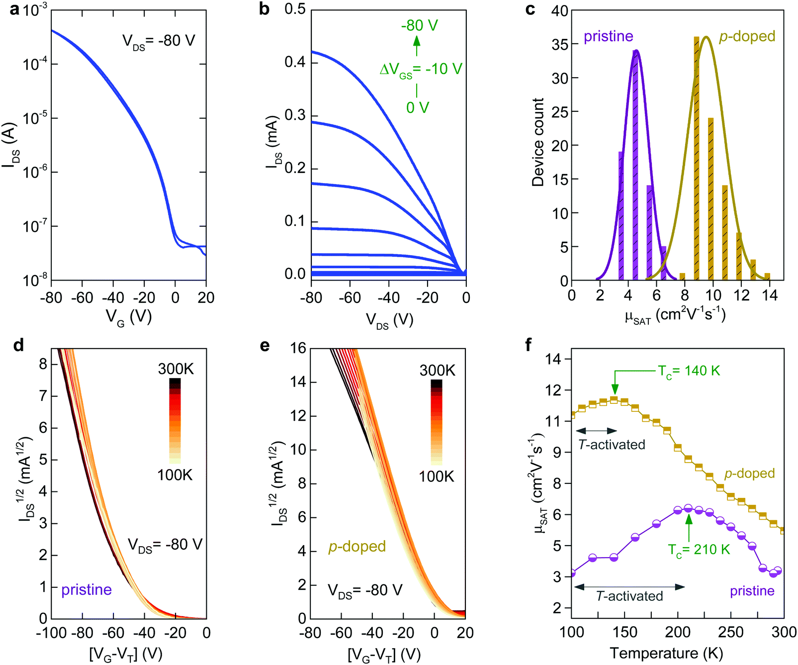 | ||
| Fig. 5 (a) Transfer and (b) output characteristics of a representative p-doped C8-BTBT:C16IDT-BT-based OTFT processed via blade-coating. (c) Histogram of the hole mobility measured in saturation (μSAT) for pristine and p-doped blend OTFTs. (d and e) Plots of the square root of the channel current (IDS0.5) versus VGS measured at different temperatures in the range 100–300 K for pristine and p-doped OTFTs prepared by blade-coating. (f) Dependence of μSAT on temperature for pristine and p-doped blend OTFTs calculated form the data in (d) and (e). The channel width and length for all devices studied were 1000 μm and 80 μm, respectively. | ||
The large difference in hole mobility values between the pristine and p-doped blend OTFTs in Fig. 5c most likely indicates different transport mechanisms. Numerous high mobility organic semiconductors were shown to exhibit a characteristic increase in charge carrier mobility with reducing temperature (band-like behaviour) and was described by invoking a dynamic disorder model.59–61 Nevertheless, for the vast majority of these molecular systems, this transport regime occurs at relatively high temperatures and above a critical temperature (TC). Below this characteristic temperature, thermal activation sets-in. The cross-over between the two transport regimes is typically understood in terms of charge carrier localization due to the presence of shallow traps, which tend to dominate charge transport at low temperatures. The origin of these trap states can differ for different materials and may relate to structural defects, grain-boundaries and on the presence of chemical impurities.62 If the extent of the disorder is reduced (i.e. reducing the trap density) the cross-over between band-like and thermally activated transport is shifted to lower temperatures and the activation energy (Ea) reduces.63 In the case of the polycrystalline layers studied here, however, the grain boundaries present between crystalline domains are known to be the source of the structural disorder64 and it remains to be seen whether p-type doping plays a role. For single-crystalline C8-BTBT-based OTFTs where such grain boundaries are largely absent, band-like transport has indeed been observed.65
Fig. 5d and e displays the IDS1/2vs. VGS plots measured at different temperatures for pristine and p-doped blend OTFTs processed via blade-coating. Interestingly, both types of devices exhibit band-like transport for temperatures above TC. At T < TC, the hole mobility becomes thermally activated in both pristine and p-doped transistors, but with the two exhibiting different EA values. Similar trends have been reported for various organic semiconductors and associated with the presence of structural disorder in the active layers.62,63,65 A noticeable difference between the two samples is seen both in terms of TC and EA values. In particular, pristine OTFTs show a TC of 210 K while for the p-doped devices the TC drops to ≈140 K, with a simultaneous decrease of the EA measured below TC. Specifically, pristine OTFTs exhibit an activation energy of ≈52.6 meV, while C60F48-doped transistors show a significantly reduced EA of ≈29.4 meV. This observation, again, suggests that inclusion of C60F48 at optimal concentrations in the blend leads to reduced energetic disorder and improved charge transport. These observations are in line with the microstructural analysis which shows that the combination of p-doping and blade-coating improves the structural quality of the resulting blend layers, ultimately resulting in the greatly improved hole-transport seen in Fig. 5f.
3. Conclusions
We have studied the influence of molecular p-doping on hole-transport in small-molecule:polymer blend OTFTs processed via conventional spin-coating and the industry-relevant technique of blade-coating. OTFTs prepared by blade-coating are found to consistently outperformed those prepared via spin-coating yielding a maximum hole mobility of 14 cm2 V−1 s−1. Irrespective of the deposition method, the blend layers exhibit a vertically phase-separated microstructure where the C8-BTBT segregates atop a C16IDT-BT-dominant phase. Introducing the molecular dopant C60F48 in the semiconducting blend was found to p-dope the formed layers, but also affects the crystallization kinetics of C8-BTBT phase leading to enhanced in-plane molecular packing of the C8-BTBT component, as corroborated by 2D GIWAXS and AFM measurements, ultimately resulting to a higher hole mobility. The work highlights the compatibility of high mobility organic semiconducting blends with high throughput printing techniques relevant to numerous emerging technologies.4. Experimental
4.1. Material preparation and device fabrication
C8-BTBT was purchased from 1-Material and used as received. Molecular dopant C60F48 was synthesized from C60 and molecular fluorine, F2, using a modified method described elsewhere.66 Its purity of 98 mol% was confirmed by 19F NMR, mass spectrometry and high performance liquid chromatography. The solution formulations were prepared using previously reported protocols.16 In brief, we used a weight ratio of C8-BTBT to C16IDT-BT of 1![[thin space (1/6-em)]](https://www.rsc.org/images/entities/char_2009.gif) :3 with a total solid content of 10 mg per ml−1 of solvent. The solution was prepared in a chlorobenzene and tetralin (1:1) mix solvent. The blend was doped with four different concentration of C60F48 dopant (0.1, 0.75, 2 and 4.25 mol%). OTFTs were fabricated with a top-gate, bottom-contact (TG-BC) architecture onto 2.54 × 2.54 cm2 large glass substrates. The Al/Au (5/35 nm) source and drain electrodes were vapor deposited using shadow mask on the glass substrates and were further treated with the contact modifier Pentafluorothiophenol (PFBT) monolayer. The blend semiconducting layers were deposited using spin-coating and blade-coating. Previously reported experimental conditions were used for the spin-coated films.17 For blade-coating, the blend solutions were coated on the substrates at 70 °C with the blade speed of 50 mm s−1. The films where then subjected to an additional annealing step at 120 °C for 1 min. A ≈900 nm-thick CYTOP film was deposited on top of the blend semiconductor by spin-coating at 2000 rpm followed by annealing at 50 °C for 1 h in nitrogen atmosphere. The geometrical capacitance of the CYTOP layers was measured to be ≈2.1 nF cm−2. Finally, a 70 nm-thick Al layer was vapor deposited atop serving as the gate electrode. The digital photographs of spin-coated and blade-coated devices are shown in Fig. S8 (ESI†) along with the device dimensions and source–drain (S–D) electrode distribution. Electrical transistor characterisation was performed using a Keysight B2912A Precision Source/Measure Unit.
:3 with a total solid content of 10 mg per ml−1 of solvent. The solution was prepared in a chlorobenzene and tetralin (1:1) mix solvent. The blend was doped with four different concentration of C60F48 dopant (0.1, 0.75, 2 and 4.25 mol%). OTFTs were fabricated with a top-gate, bottom-contact (TG-BC) architecture onto 2.54 × 2.54 cm2 large glass substrates. The Al/Au (5/35 nm) source and drain electrodes were vapor deposited using shadow mask on the glass substrates and were further treated with the contact modifier Pentafluorothiophenol (PFBT) monolayer. The blend semiconducting layers were deposited using spin-coating and blade-coating. Previously reported experimental conditions were used for the spin-coated films.17 For blade-coating, the blend solutions were coated on the substrates at 70 °C with the blade speed of 50 mm s−1. The films where then subjected to an additional annealing step at 120 °C for 1 min. A ≈900 nm-thick CYTOP film was deposited on top of the blend semiconductor by spin-coating at 2000 rpm followed by annealing at 50 °C for 1 h in nitrogen atmosphere. The geometrical capacitance of the CYTOP layers was measured to be ≈2.1 nF cm−2. Finally, a 70 nm-thick Al layer was vapor deposited atop serving as the gate electrode. The digital photographs of spin-coated and blade-coated devices are shown in Fig. S8 (ESI†) along with the device dimensions and source–drain (S–D) electrode distribution. Electrical transistor characterisation was performed using a Keysight B2912A Precision Source/Measure Unit.
4.2. Field-effect charge carrier mobility calculations
The field-effect charge carrier mobility was calculated from the transfer characteristics of the transistors in the saturation regime using.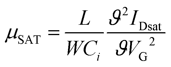 | (1) |
In eqn (1), L and W are the transistor channel length and width respectively, VG is the applied gate voltage, Ci the geometrical capacitance of the gate dielectric employed, and IDsat the channel current measured in saturation.
4.3. Polarized optical microscopy
Nikon LV-100 microscope was used to perform high speed POM and the images were recorded using a Photron SA-3 CMOS camera.4.4. Atomic force microscopy
An Agilent 5500 instrument was used to perform all AFM measurements. The scanning speed was set at 0.2 lines s−1. The image processing and the statistical analysis of the images were done using Gwyddion software.4.5. Transmission electron microscopy
A transmission electron microscope of model Titan G2 80-300 ST from Thermo-Fisher Scientific was used to perform the cross-sectional TEM (X-TEM) analysis of the samples. The TEM instrument is equipped with a spherical aberration corrector for the condenser lens and an energy-filter GIF-Quantum 966 from Gatan Inc. for aberration corrected scanning TEM (AC-STEM) and electron energy loss spectroscopy (EELS), respectively. Further, the microscope was operated at the accelerating voltage of 300 kV and in STEM mode during the analysis of the samples. The AC-STEM images were generated by collecting the transmitted electron beam with a retractable analogue high angular annular dark-field (HAADF) detector installed above the projection chamber of the microscope. The morphology and thickness of each layer in the stacks was investigated by acquiring the HAADF-STEM images at various magnifications. Whereas, the elemental maps of the main constituents namely, sulphur (S), carbon (C), and oxygen (O) were generated by acquiring the EELS datasets from the samples in a synchronized fashion during the STEM imaging. Furthermore, the elemental maps of S, C, and O were generated by acquiring their S–L23, C–K, and O–K energy-loss edges at the energy of 165 eV, 283 eV, and 532 eV, respectively. In this way, the STEM-EELS data-cubes were acquired and processed to generate individual as well as RGB Composite elemental maps.4.6. Grazing-incidence wide-angle X-ray scattering
Wide-angle X-ray scattering (GIWAXS) measurements were performed at the non-crystalline diffraction beamline (BL11-NCD-Sweet) at ALBA Synchrotron Radiation Facility in Barcelona (Spain). A Rayonix, WAXS LX255-HS detector was used to collect the scattering signals, resolution: 1920 × 5760 pixels (pixel size = 40 × 40 μm2). Data are expressed as a function of the scattering vector (q) and the angle of incidence was 0.1°. GIWAXS patterns were corrected as a function of the components of the scattering vector with a Matlab script designed for this purpose.67 Integrations have been done with Fit2D software.Conflicts of interest
There are no conflicts to declare.Acknowledgements
This publication is based upon work supported by the King Abdullah University of Science and Technology (KAUST) Office of Sponsored Research (OSR) under Award No: RPE/1/4196-01. The authors would like to thank ALBA synchrotron and staff for their help with the GIWAXS measurements.References
- H. Sun, Q. Wang, J. Qian, Y. Yin, Y. Shi and Y. Li, Semicond. Sci. Technol., 2015, 30, 054001 CrossRef.
- S. D. Brotherton and S. D. Brotherton, Introduction to Thin Film Transistors, Springer International Publishing, 2013, pp. 185–251 Search PubMed.
- S. Wang, J. Xu, W. Wang, G. J. N. Wang, R. Rastak, F. Molina-Lopez, J. W. Chung, S. Niu, V. R. Feig, J. Lopez, T. Lei, S. K. Kwon, Y. Kim, A. M. Foudeh, A. Ehrlich, A. Gasperini, Y. Yun, B. Murmann, J. B. H. Tok and Z. Bao, Nature, 2018, 555, 83–88 CrossRef CAS.
- Y. Yuan, G. Giri, A. L. Ayzner, A. P. Zoombelt, S. C. B. Mannsfeld, J. Chen, D. Nordlund, M. F. Toney, J. Huang and Z. Bao, Nat. Commun., 2014, 5, 3005 CrossRef.
- Y. Diao, B. C. K. Tee, G. Giri, J. Xu, D. H. Kim, H. A. Becerril, R. M. Stoltenberg, T. H. Lee, G. Xue, S. C. B. Mannsfeld and Z. Bao, Nat. Mater., 2013, 12, 665–671 CrossRef CAS.
- R. R. Søndergaard, M. Hösel and F. C. Krebs, J. Polym. Sci., Part B: Polym. Phys., 2013, 51, 16–34 CrossRef.
- H. A. Becerril, M. E. Roberts, Z. Liu, J. Locklin and Z. Bao, Adv. Mater., 2008, 20, 2588–2594 CrossRef CAS.
- P. Yadav, C. Chanmal, A. Basu, L. Mandal, J. Jog and S. Ogale, RSC Adv., 2013, 3, 18049–18054 RSC.
- B. Peng, X. Ren, Z. Wang, X. Wang, R. C. Roberts and P. K. L. Chan, Sci. Rep., 2014, 4, 6430 CrossRef CAS.
- H. Li, B. C. K. Tee, J. J. Cha, Y. Cui, J. W. Chung, S. Y. Lee and Z. Bao, J. Am. Chem. Soc., 2012, 134, 2760–2765 CrossRef CAS.
- Y. Lee, J. Y. Oh, T. R. Kim, X. Gu, Y. Kim, G. J. N. Wang, H. C. Wu, R. Pfattner, J. W. F. To, T. Katsumata, D. Son, J. Kang, J. R. Matthews, W. Niu, M. He, R. Sinclair, Y. Cui, J. B. H. Tok, T. W. Lee and Z. Bao, Adv. Mater., 2018, 30(7), 1704401 CrossRef.
- R. H. Kim, H. J. Kim, I. Bae, S. K. Hwang, D. B. Velusamy, S. M. Cho, K. Takaishi, T. Muto, D. Hashizume, M. Uchiyama, P. André, F. Mathevet, B. Heinrich, T. Aoyama, D. E. Kim, H. Lee, J. C. Ribierre and C. Park, Nat. Commun., 2014, 5, 3583 CrossRef.
- G. Gelinck, P. Heremans, K. Nomoto and T. D. Anthopoulos, Adv. Mater., 2010, 22, 3778–3798 CrossRef CAS.
- H. Matsui, Y. Takeda and S. Tokito, Org. Electron., 2019, 75, 105432 CrossRef CAS.
- E. Menard, V. Podzorov, S. H. Hur, A. Gaur, M. E. Gershenson and J. A. Rogers, Adv. Mater., 2004, 16, 2097–2101 CrossRef CAS.
- A. F. Paterson, N. D. Treat, W. Zhang, Z. Fei, G. Wyatt-Moon, H. Faber, G. Vourlias, P. A. Patsalas, O. Solomeshch, N. Tessler, M. Heeney and T. D. Anthopoulos, Adv. Mater., 2016, 28, 7791–7798 CrossRef CAS.
- A. F. Paterson, L. Tsetseris, R. Li, A. Basu, H. Faber, A. Emwas, J. Panidi, Z. Fei, M. R. Niazi, D. H. Anjum, M. Heeney and T. D. Anthopoulos, Adv. Mater., 2019, 31, 1900871 CrossRef.
- A. F. Paterson, S. Singh, K. J. Fallon, T. Hodsden, Y. Han, B. C. Schroeder, H. Bronstein, M. Heeney, I. McCulloch and T. D. Anthopoulos, Adv. Mater., 2018, 30 Search PubMed.
- W. Pisula, A. Menon, M. Stepputat, I. Lieberwirth, U. Kolb, A. Tracz, H. Sirringhaus, T. Pakula and K. Müllen, Adv. Mater., 2005, 17, 684–688 CrossRef CAS.
- R. L. Headrick, S. Wo, F. Sansoz and J. E. Anthony, Appl. Phys. Lett., 2008, 92, 063302 CrossRef.
- C. M. Duffy, J. W. Andreasen, D. W. Breiby, M. M. Nielsen, M. Ando, T. Minakata and H. Sirringhaus, Chem. Mater., 2008, 20, 7252–7259 CrossRef CAS.
- D. Khim, H. Han, K. J. Baeg, J. Kim, S. W. Kwak, D. Y. Kim and Y. Y. Noh, Adv. Mater., 2013, 25, 4302–4308 CrossRef CAS.
- M. R. Niazi, R. Li, E. Qiang Li, A. R. Kirmani, M. Abdelsamie, Q. Wang, W. Pan, M. M. Payne, J. E. Anthony, D. M. Smilgies, S. T. Thoroddsen, E. P. Giannelis and A. Amassian, Nat. Commun., 2015, 6, 8598 CrossRef CAS.
- K. Kim, J. Hong, S. G. Hahm, Y. Rho, T. K. An, S. H. Kim and C. E. Park, ACS Appl. Mater. Interfaces, 2019, 11, 13481–13490 CrossRef CAS.
- R. L. Davis, S. Jayaraman, P. M. Chaikin and R. A. Register, Langmuir, 2014, 30, 5637–5644 CrossRef CAS.
- M. Richard, A. Al-Ajaji, S. Ren, A. Foti, J. Tran, M. Frigoli, B. Gusarov, Y. Bonnassieux, E. G. Caurel, P. Bulkin, R. Ossikovski and A. Yassar, Adv. Colloid Interface Sci., 2020, 275 Search PubMed.
- M. Chen, B. Peng, S. Huang and P. K. L. Chan, Adv. Funct. Mater., 2020, 30, 1905963 CrossRef CAS.
- K. Haase, C. Teixeira da Rocha, C. Hauenstein, Y. Zheng, M. Hambsch and S. C. B. Mannsfeld, Adv. Electron. Mater., 2018, 4, 1–9 CAS.
- S. Arai, S. Inoue, T. Hamai, R. Kumai and T. Hasegawa, Adv. Mater., 2018, 30, 1707256 CrossRef.
- G. Giri, E. Verploegen, S. C. B. Mannsfeld, S. Atahan-Evrenk, D. H. Kim, S. Y. Lee, H. A. Becerril, A. Aspuru-Guzik, M. F. Toney and Z. Bao, Nature, 2011, 480, 504–508 CrossRef CAS.
- F. G. Del Pozo, S. Fabiano, R. Pfattner, S. Georgakopoulos, S. Galindo, X. Liu, S. Braun, M. Fahlman, J. Veciana, C. Rovira, X. Crispin, M. Berggren and M. Mas-Torrent, Adv. Funct. Mater., 2016, 26, 2379–2386 CrossRef CAS.
- Z. Zhang, B. Peng, X. Ji, K. Pei and P. K. L. Chan, Adv. Funct. Mater., 2017, 27, 1703443 CrossRef.
- A. Yamamura, S. Watanabe, M. Uno, M. Mitani, C. Mitsui, J. Tsurumi, N. Isahaya, Y. Kanaoka, T. Okamoto and J. Takeya, Sci. Adv., 2018, 4, eaao5758 CrossRef.
- B. Peng, S. Huang, Z. Zhou and P. K. L. Chan, Adv. Funct. Mater., 2017, 27, 1700999 CrossRef.
- Y. Abe, T. Hasegawa, Y. Takahashi, T. Yamada and Y. Tokura, Appl. Phys. Lett., 2005, 87, 1–3 Search PubMed.
- K. Zhao, O. Wodo, D. Ren, H. U. Khan, M. R. Niazi, H. Hu, M. Abdelsamie, R. Li, E. Q. Li, L. Yu, B. Yan, M. M. Payne, J. Smith, J. E. Anthony, T. D. Anthopoulos, S. T. Thoroddsen, B. Ganapathysubramanian and A. Amassian, Adv. Funct. Mater., 2016, 26, 1737–1746 CrossRef CAS.
- C. Teixeira da Rocha, K. Haase, Y. Zheng, M. Löffler, M. Hambsch and S. C. B. Mannsfeld, Adv. Electron. Mater., 2018, 4(8), 1800141 CrossRef.
- G. Zhang, H. Yang, L. He, L. Hu, S. Lan, F. Li, H. Chen and T. Guo, J. Polym. Sci., Part B: Polym. Phys., 2016, 54, 1760–1766 CrossRef CAS.
- J. Smith, R. Hamilton, I. McCulloch, N. Stingelin-Stutzmann, M. Heeney, D. D. C. Bradley and T. D. Anthopoulos, J. Mater. Chem., 2010, 20, 2562–2574 RSC.
- A. D. Scaccabarozzi and N. Stingelin, J. Mater. Chem. A, 2014, 2, 10818–10824 RSC.
- S. Scheinert, G. Paasch, S. Pohlmann, H. H. Hörhold and R. Stockmann, Solid-State Electron., 2000, 44, 845–853 CrossRef CAS.
- J. H. Oh, P. Wei and Z. Bao, Appl. Phys. Lett., 2010, 97, 243305 CrossRef.
- L. Ma, W. H. Lee, Y. D. Park, J. S. Kim, H. S. Lee and K. Cho, Appl. Phys. Lett., 2008, 92, 063310 CrossRef.
- C. T. Lee and H. C. Chen, Org. Electron., 2011, 12, 1852–1857 CrossRef CAS.
- E. Lim, B. J. Jung, M. Chikamatsu, R. Azumi, Y. Yoshida, K. Yase, L. M. Do and H. K. Shim, J. Mater. Chem., 2007, 17, 1416–1420 RSC.
- S. Riera-Galindo, F. Leonardi, R. Pfattner and M. Mas-Torrent, Adv. Mater. Technol., 2019, 4, 1900104 CrossRef CAS.
- R. Hamilton, J. Smith, S. Ogier, M. Heeney, J. E. Anthony, I. McCulloch, J. Veres, D. D. C. Bradley and T. D. Anthopoulos, Adv. Mater., 2009, 21, 1166–1171 CrossRef CAS.
- J. Smith, W. Zhang, R. Sougrat, K. Zhao, R. Li, D. Cha, A. Amassian, M. Heeney, I. McCulloch and T. D. Anthopoulos, Adv. Mater., 2012, 24, 2441–2446 CrossRef CAS.
- X. Gu, L. Shaw, K. Gu, M. F. Toney and Z. Bao, Nat. Commun., 2018, 9 CAS.
- M. Le Berre, Y. Chen and D. Baigl, Langmuir, 2009, 25, 2554–2557 CrossRef CAS.
- Y. Diao, L. Shaw, Z. Bao and S. C. B. Mannsfeld, Energy Environ. Sci., 2014, 7, 2145–2159 RSC.
- K. Zhao, O. Wodo, D. Ren, H. U. Khan, M. R. Niazi, H. Hu, M. Abdelsamie, R. Li, E. Q. Li, L. Yu, B. Yan, M. M. Payne, J. Smith, J. E. Anthony, T. D. Anthopoulos, S. T. Thoroddsen, B. Ganapathysubramanian and A. Amassian, Adv. Funct. Mater., 2016, 26, 1737–1746 CrossRef CAS.
- A. F. Paterson, Y.-H. Lin, A. D. Mottram, Z. Fei, M. R. Niazi, A. R. Kirmani, A. Amassian, O. Solomeshch, N. Tessler, M. Heeney and T. D. Anthopoulos, Adv. Electron. Mater., 2018, 4, 1700464 CrossRef.
- H. I. Un, J. Y. Wang and J. Pei, Adv. Sci., 2019, 6, 1900375 CrossRef CAS.
- H. Sirringhaus, Adv. Mater., 2005, 17, 2411–2425 CrossRef CAS.
- S. Zafar, A. Callegari, E. Gusev and M. V. Fischetti, J. Appl. Phys., 2003, 93, 9298 CrossRef CAS.
- I. Amit, T. J. Octon, N. J. Townsend, F. Reale, C. D. Wright, C. Mattevi, M. F. Craciun and S. Russo, Adv. Mater., 2017, 29, 1605598 CrossRef.
- A. F. Paterson, Y. H. Lin, A. D. Mottram, Z. Fei, M. R. Niazi, A. R. Kirmani, A. Amassian, O. Solomeshch, N. Tessler, M. Heeney and T. D. Anthopoulos, Adv. Electron. Mater., 2017, 4(10), 1700464 CrossRef.
- S. Ciuchi, S. Fratini and D. Mayou, Phys. Rev. B: Condens. Matter Mater. Phys., 2015, 83(8), 081202 CrossRef.
- Y. C. Cheng and R. J. Silbey, J. Chem. Phys., 2003, 118, 3764–3774 CrossRef CAS.
- J. D. Picon, M. N. Bussac and L. Zuppiroli, Phys. Rev. B: Condens. Matter Mater. Phys., 2007, 75(23), 235106 CrossRef.
- H. Sirringhaus, T. Sakanoue and J. F. Chang, Phys. Status Solidi B, 2012, 249, 1655–1676 CrossRef CAS.
- N. A. Minder, S. Lu, S. Fratini, S. Ciuchi, A. Facchetti and A. F. Morpurgo, Adv. Mater., 2014, 26, 1254–1260 CrossRef CAS.
- J. Smith, R. Hamilton, I. McCulloch, N. Stingelin-Stutzmann, M. Heeney, D. D. C. Bradley and T. D. Anthopoulos, J. Mater. Chem., 2010, 20, 2562–2574 RSC.
- J. M. Cho, T. Higashino and T. Mori, Appl. Phys. Lett., 2015, 106, 1–5 Search PubMed.
- O. V. Boltalina and N. A. Galeva, Usp. Khim., 2000, 69, 673–674 Search PubMed.
- A. Nogales and E. Gutiérrez, 2D Representation of a Wide Angle X Ray Scattering pattern as a function of Q vector components, https://jp.mathworks.com/matlabcentral/fileexchange/71958-grazing-incidence-wide-angle-x-ray-scattering-representation, accessed 10 March 2020.
Footnote |
| † Electronic supplementary information (ESI) available: Transistor measurements, transistor parameter distribution, atomic force microscopy, GIWAXS analysis. See DOI: 10.1039/d0tc03094e |
| This journal is © The Royal Society of Chemistry 2020 |