
A high performance UV–visible dual-band photodetector based on an inorganic Cs2SnI6 perovskite/ZnO heterojunction structure
Dali
Shao
 *a,
Weiguang
Zhu
b,
Guoqing
Xin
b,
Xueqing
Liu
a,
Tianmeng
Wang
ac,
Sufei
Shi
ac,
Jie
Lian
*b and
Shayla
Sawyer
*a
*a,
Weiguang
Zhu
b,
Guoqing
Xin
b,
Xueqing
Liu
a,
Tianmeng
Wang
ac,
Sufei
Shi
ac,
Jie
Lian
*b and
Shayla
Sawyer
*a
aDepartment of Electrical, Computer, and Systems Engineering, Rensselaer Polytechnic Institute, Troy, NY 12180, USA. E-mail: shaodali828@gmail.com; sawyes@rpi.edu
bDepartment of Mechanical, Aerospace and Nuclear Engineering, Rensselaer Polytechnic Institute, Troy, NY 12180, USA. E-mail: lianj@rpi.edu
cDepartment of Chemical and Biological Engineering, Rensselaer Polytechnic Institute, Troy, NY 12180, USA
First published on 11th December 2019
Abstract
Inorganic metal halide (IMH) perovskites have recently emerged as highly promising optoelectronic materials due to their excellent material properties, including tunable direct bandgap, long carrier diffusion length, high carrier mobility and outstanding environmental stabilities. However, the performance of photodetectors fabricated from IMH perovskites so far is limited as compared to their counterparts based on organic–inorganic hybrid perovskites. In this work, we demonstrate a high performance ultraviolet–visible (UV–Vis) dual-band photodetector based on a Cs2SnI6/ZnO heterojunction structure. By adjusting the polarity of the applied bias voltage, the photodetector can switch between two operation modes: (1) UV–Vis dual-band detection mode and (2) visible-blind UV detection mode. High detectivity in both the UV (1.39 × 10¹² Jones) and visible (5.88 × 10¹¹ Jones) regions is achieved. In addition, this photodetector demonstrated a fast response speed with a rise and fall time on the order of milliseconds and a large linear dynamic range of 119 dB. The excellent performance of this photodetector originates from efficient charge separation at the heterojunction interfaces, which will be discussed in detail in terms of the energy band diagrams and carrier dynamics of the device. Our study demonstrates the great application potential of inorganic vacancy-ordered perovskites in high-performance heterojunction photodetectors.
Introduction
Organic–inorganic hybrid perovskites have been considered to be promising for future optoelectronic applications due to their many excellent material properties including tunable direct bandgap, large optical absorption coefficients, long carrier diffusion lengths, and high carrier mobility.1–8 Indeed, significant progress has been achieved in organic–inorganic hybrid perovskite based optoelectronics including highly sensitive photodetectors, broadband tunable light-emitting diodes (LEDs), highly efficient solar cells with power conversion efficiencies exceeding 20%, etc.9–16 Nevertheless, the environmental instability of organic–inorganic hybrid perovskites is still the main concern for their practical applications. To overcome this hurdle, many all-inorganic halide perovskites have been developed as alternative materials.17–28 Among these materials, tin (Sn) based perovskites ASnX3 (X = I, Br, Cl) have attracted particular interest due to their nontoxicity and excellent optoelectronic properties.26–28 However, ASnX3 are very sensitive to the ambient atmosphere (oxygen, moisture, etc.) and easily oxidized from Sn2+ to Sn4+. Therefore, exploration of air-stable alternatives has become an urgent need. Very recently, chemically stable Sn4+ based vacancy-ordered double perovskite materials such as Cs2SnIxCl6−x and Cs2SnCl6−xBrx have been demonstrated for energy harvesting, light emitting, and narrow band light detection applications.29–31 Unfortunately, the sensitivity of photodetectors fabricated from Cs2SnCl6−xBrx single crystals is limited (<1011 Jones), and the detection range is restricted within the visible region. One possible approach for improving the performance of inorganic perovskite photodetectors is to combine the perovskite layer with other functional materials to form bilayer hetero-structures. For example, Tong et al. developed a sensitive, self-driven near infrared photodetector based on a CsBi3I10 perovskite/silicon heterojunction structure, very recently a Cs2SnCl6/GaN heterojunction photodetector has been demonstrated with excellent narrow-band sensitivity in the UV region.32,33 A major challenge in designing a heterojunction photodetector is the need to improve the photoresponse of the device while at the same time maintaining a low dark current, which is critical for achieving high detectivity. Among many of the potential semiconductor materials for constructing a heterojunction with a perovskite, ZnO is a promising candidate due to its excellent optical and electrical properties including a wide direct band gap (3.37 eV), large exciton binding energy (60 meV), high carrier mobility, and outstanding environmental stability.34,35 In fact, for the same reason, ZnO has frequently been employed as an electron transfer layer in the fabrication of perovskite solar cells.36–38 Among many different methods to grow ZnO thin films, the atomic layer deposition (ALD) technique has great potential in the fabrication of inorganic perovskite-based heterojunction photodetectors. ALD can provide thickness-controlled, dense and uniform thin films with minimum defects, which is critical to enhance the photocurrent and suppress the dark current for heterojunction optoelectronic devices.39–41 Remarkably, recent work done by G. Cen, et al. demonstrated a highly sensitive and stable CsPbBr3 perovskite heterojunction photodetector by employing ALD as a powerful interfacial engineering technique for device performance tuning and optimization.39In this work, we demonstrate a high performance UV–Vis dual-band photodetector based on a Cs2SnI6/ZnO heterojunction structure. By adjusting the polarity of the applied bias voltage, the photodetector can switch between two operation modes: (1) UV–Vis dual-band detection mode and (2) visible-blind UV detection mode. Such a unique function of this photodetector greatly extends its practical applications. Benefitting from the excellent carrier separation efficiency at the hetero-interface, the device achieved high detectivity in both UV (1.39 × 10¹² Jones) and visible (5.88 × 10¹¹ Jones) regions. Furthermore, the photodetector demonstrated a fast response speed with a rise and fall time on the order of milliseconds and a large linear dynamic range of 119 dB. The results in this work demonstrate the great application potential of inorganic vacancy-ordered perovskites in high performance heterojunction photodetectors. Further research toward this direction is highly desirable.
Results and discussion
Fig. 1a shows the three-dimensional schematic illustration of the Cs2SnI6/ZnO heterojunction photodiode. The crystal structure of the vacancy-ordered double perovskite Cs2SnI6 is illustrated in Fig. 1b, which presents a vacancy-ordered double perovskite structure with isolated [SnI6] octahedra. The scanning electron microscopy (SEM) image of the synthesized Cs2SnI6 NP thin film is shown in Fig. 1c, and the average size of the Cs2SnI6 NPs is estimated to be 20–30 nm. XRD was performed on the sample to check the crystallinity, as shown in Fig. 1d. The major peaks at the 2θ values: 13.2°, 15.2°, 21.6°, 25.4°, 26.6°, 30.8°, 44.1°, 52.0°, and 54.6°, correspond to the atomic planes of (111), (002), (022), (113), (222), (004), (044), (226), and (444), respectively. The UV–Vis absorption spectrum and the photoluminescence (PL) spectrum of the Cs2SnI6 NPs at room temperature are presented in Fig. 1e. The absorption spectrum shows a cut off wavelength at 860 nm, corresponding to an optical band gap of ∼1.4 eV. This optical band gap was further verified by PL spectroscopy. As shown in Fig. 1e, the PL spectrum excited at 520 nm exhibited a pronounced PL peak ranging from 770 to 1000 nm with the peak centered at 861 nm, confirming the effective optical band gap of ∼1.4 eV for the synthesized Cs2SnI6 NPs. This is consistent with previous literature reports, where the bandgap values vary from 1.26 to 1.6 eV.42–44 It is worth mentioning that the post growth hydrogen annealing treatment of the ALD grown ZnO thin film can greatly improve the film conductivity due to the introduction of shallow donor states such as the VO–H complex and interstitial hydrogen.45–47 In addition, the passivation effect of the post growth hydrogen annealing treatment can effectively cure the deep level defects and reduce the number of carrier scattering centers in the ZnO thin film, leading to improved electron mobility.48 As demonstrated in Fig. 1f, the photoluminescence spectrum of the ZnO thin film after the hydrogen annealing treatment shows greatly enhanced band-edge UV emission centered at ∼375 nm and suppressed defect level green emission centered at ∼600 nm.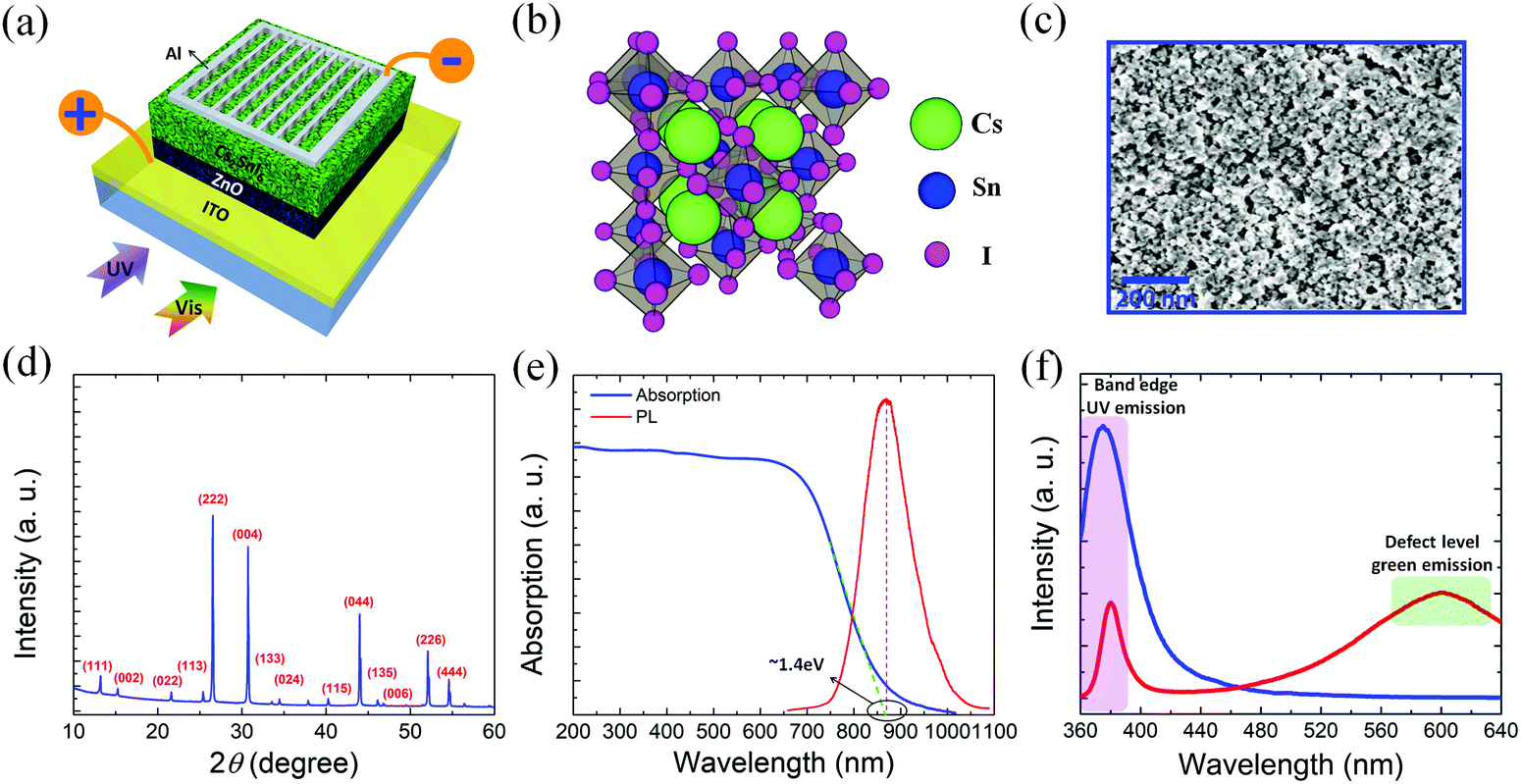 | ||
| Fig. 1 (a) Schematic illustration of the Cs2SnI6/ZnO heterojunction photodiode. (b) Schematic illustration showing the crystal structure of the vacancy-ordered double perovskite Cs2SnI6. (c) SEM image of the Cs2SnI6 NP thin film. (d) XRD pattern of the synthesized Cs2SnI6 NPs. (e) UV–Vis absorption spectrum and PL spectrum of the synthesized Cs2SnI6 NPs. (f) PL spectra of the ALD grown ZnO thin film before (red line) and after (blue line) hydrogen annealing. | ||
The I–V characteristics of the photodetector are measured in the dark, under 760 nm visible illumination, and under 375 nm UV illumination, as shown in Fig. 2a. The dark current of the heterojunction photodiode shows an excellent rectifying characteristic with a high rectification ratio of 161 when biased at ±5 V. When forward biased, the dark current increases exponentially following the equation I ∼ exp(αV). The constant α is calculated to be 0.34 V−1 by fitting the experimental data. Under reverse bias, the photocurrent generated by 760 nm visible/375 nm UV illumination is over 500 times/three orders of magnitude higher than the dark current, demonstrating a good signal to noise ratio of this device in both the UV and visible region. Under forward bias, however, the photocurrent generated by 375 nm UV light is less than two orders of magnitude higher than the dark current, and the photocurrent generated by 760 nm visible light is almost comparable to the dark current, suggesting a complete quenching of the photoresponse in the visible region. Such a kind of voltage polarity dependent photosensitivity will be discussed in detail later in this paper. The transient photoresponse of this device was measured under a 375 nm short pulse light from a LED, as presented in Fig. 3f. The rise time (output signal changing from 10% to 90% of the peak output value) and the decay time (output signal changing from 90% to 10% of the peak output value) of the photocurrent are 4.3 μs and 5.2 μs, respectively. This is faster than most of the perovskite based photodetectors reported so far, indicating good quality of the ZnO thin film and the Cs2SnI6 NPs.
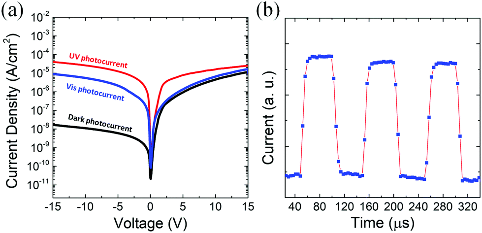 | ||
| Fig. 2 (a) I–V characteristics of the photodetector measured in the dark, under 760 nm visible illumination, and 375 nm UV illumination. (b) Transient response of the heterojunction photodiode with a rising time of 4.3 μs and a falling time of 5.2 μs measured under ambient conditions. | ||
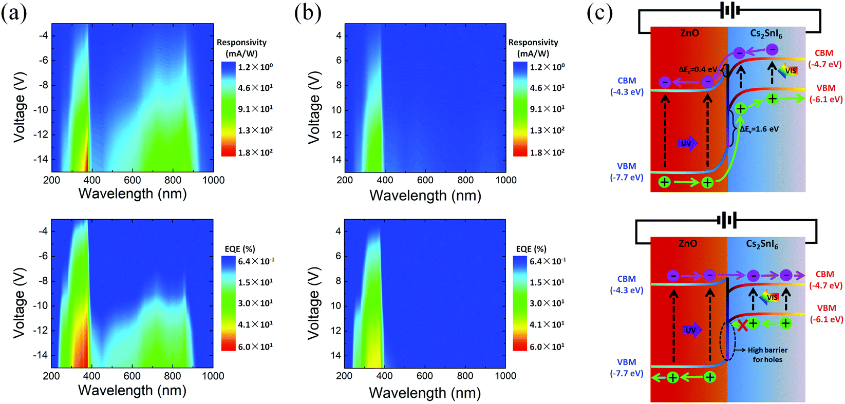 | ||
| Fig. 3 (a) Photoresponsivity (top) and EQE (bottom) pseudo-color maps of this heterojunction photodiode measured under reverse bias voltages. (b) Photoresponsivity (top) and EQE (bottom) pseudo-color maps of this heterojunction photodiode measured under forward bias voltages. (c) Schematic energy band diagram showing the band alignment and carrier dynamics of this device operating under reverse bias (top) and forward bias (bottom) conditions. | ||
Photoresponsivity is an important figure-of-merit for photodetectors, which is defined as the photocurrent per unit of incident optical power. The photoresponsivity and EQE pseudo-color maps of this heterojunction photodiode measured under reverse bias and forward bias conditions are shown in Fig. 3a and b, respectively. As shown in Fig. 3a, the photoresponsivity and EQE pseudo-color maps of this device under reverse bias show two major detection bands. The first detection band is contributed by the ZnO layer and is located in the UV region from 280 nm to 385 nm. A maximum photoresponsivity of 183.4 mA W−1 was measured at 378 nm wavelength, corresponding to an EQE of 60.2%. The second detection band located in the visible region from ∼600–900 nm is mainly contributed by the Cs2SnI6 layer. A maximum responsivity of 113.4 mA W−1 was measured at 858 nm (1.44 eV) wavelength, which agrees well with the bandgap of Cs2SnI6 (1.4 eV) measured in this work. Under forward bias, however, only the UV detection band remains while the visible detection band was completely quenched, as shown in Fig. 3b. A maximum responsivity of 108 mA W−1 at 374 nm was measured under forward bias, lower than that measured under reverse bias conditions. To understand this voltage polarity dependent photoresponse, we can refer to the schematic energy band diagram of this heterojunction shown in Fig. 3c. Based on the Anderson's model, the Cs2SnI6/ZnO heterojunction has a small conduction band offset of 0.4 eV and a large valence band offset of 1.6 eV. Since ZnO is highly transparent to visible light, most of the visible light can get through ZnO and be absorbed in the Cs2SnI6 film to generate electron-hole pairs (EHPs). Under reversed bias conditions, the photogenerated electrons at the Cs2SnI6 side can transport through the interfacial barrier easily (due to the small conduction band offset) and drift toward the contact at the ZnO thin film side driven by an external electrical field. At the same time, the photogenerated holes in both ZnO and Cs2SnI6 drift toward the contact at the Cs2SnI6 side without any energy barriers. Therefore, the photogenerated electrons and holes in both ZnO and Cs2SnI6 can be collected to form the photocurrent signal, resulting in the UV–Vis dual detection band. In contrast, when the heterojunction is forward biased, the photogenerated holes in the Cs2SnI6 side tend to drift toward the ZnO region under an external electrical field but they cannot get through the interfacial region due to the high energy barrier (1.6 eV) present for holes. Therefore, without any efficient charge separation at the hetero-interface under forward bias, the photogenerated holes in the Cs2SnI6 quickly recombine with the photogenerated electrons, leading to the significant quenching of the photoresponse in the visible band. Therefore, by adjusting the polarity of external bias, our device can operate in either the UV–Vis dual detection band mode or the visible-blind UV detection mode. This function greatly extends the photodetector's practical applications including secure space-to-space communications, pollution monitoring, water sterilization, flame sensing, early missile plume detection, security surveillance, etc.
Detectivity (D*) is an important parameter that indicates the ability of a photodetector to measure weak optical signals. The D* is expressed as:49,50
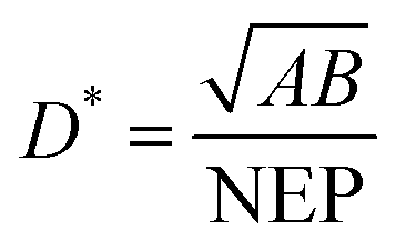
where e is the element charge and id is the dark current of the device, and the thermal noise in,t can be expressed as:
where kB is the Boltzmann constant, T is the temperature, and R is the resistance of the device. The shot noise limit and thermal noise limit of this device are plotted in Fig. 4b. Clearly, the total noise of this device is mainly dominated by the shot noise. In the UV region, a maximum specific detectivity of 1.39 × 10¹² Jones was achieved at 378 nm and in the visible region, a maximum detectivity of 5.88 × 10¹¹ Jones was measured at 858 nm, demonstrating excellent sensitivity of this heterojunction photodetector in both the UV and visible region. It is worth mentioning that the performance of the photodetector could be further improved through optimization of the Cs2SnI6 and ZnO layer thickness, which impacts the carrier recombination rate, carrier collection efficiency, and response speed of the photodetector.
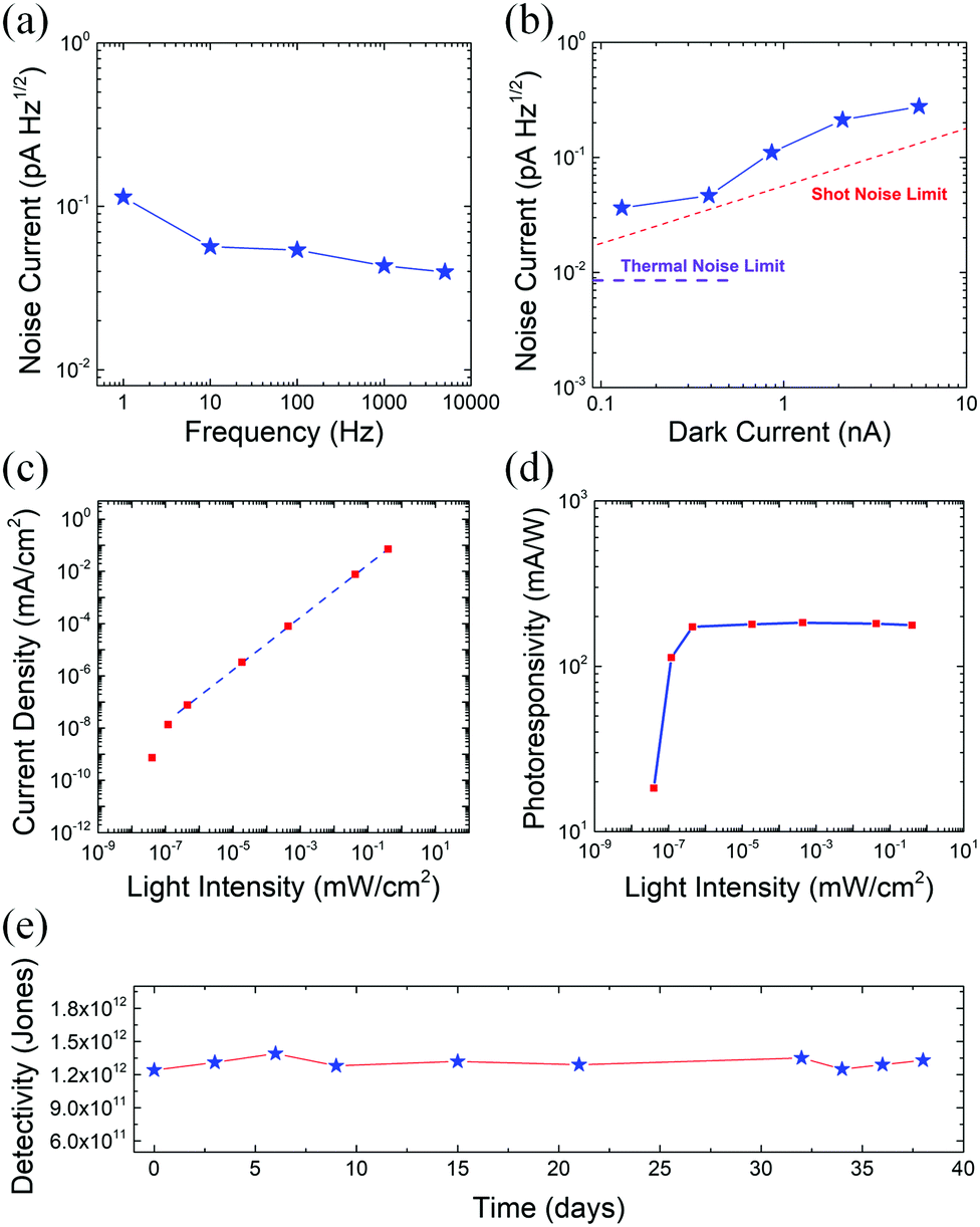 | ||
| Fig. 4 (a) Noise current measured at various frequencies in the range from 1 Hz to 5 kHz. (b) Noise current measured at different dark current levels. (c) Photocurrent density measured at varying light intensities. (d) The consistency of the photoresponsivity measured over a wide range of light intensity. (e) The detectivity of the photodetector measured over time. | ||
In addition to the high detectivity, a constant responsivity from strong light all the way down to weak light is important for a detector so that it can be applied for weak light sensing. Every photodetector has a finite range of linear response and is characterized by a linear dynamic range, in which the responsivity remains constant. LDR is expressed as:49,50
| Device structure | Measurement wavelength [nm] | Maximum responsivity [mA W−1] | Rise/decay time [μs] | Detectivity [Jones] | LDR [dB] | Ref. |
|---|---|---|---|---|---|---|
| SnO2/CsPbBr3 | 300 | 380 | N/A | 2.6 × 10¹¹ | N/A | 52 |
| Cs2SnCl6/GaN | 378 | 208 | 0.75/0.91 | 1.2 × 10¹² | 71 | 33 |
| CsPbBr3/ZnO | 450 | 4250 | 210/240 | N/A | N/A | 36 |
| CsBi3I10/silicon | 808 | 492.1 | 73/76 | 1.38 × 10¹¹ | N/A | 32 |
| CsPbBr3/InGaZnO | 365 | 3794 | 2000/2000 | NA | N/A | 53 |
| Al2O3/CsPbBr3/TiO2 | 405 | 440 | 28/270 | 1.88 × 10¹³ | ∼173 | 39 |
| Cs2SnI6/ZnO | 378 | 183.4 | 4.3/5.2 | 1.39 × 10¹² | 119 | This work |
Conclusions
In conclusion, we demonstrated a Cs2SnI6/ZnO heterojunction photodetector with a high performance UV–Vis dual-band sensing capability. The photodetector can switch between the UV–Vis dual-band detection mode and visible-blind UV detection mode by adjusting the polarity of the external bias. This unique function of this photodetector greatly extends its practical applications. Benefitting from the excellent carrier separation efficiency at the hetero-interface, the device achieved high detectivity in both the UV (1.39 × 10¹² Jones) and visible (5.88 × 10¹¹ Jones) regions under reverse bias conditions. Furthermore, the photodetector demonstrated a fast response speed with a rise and fall time on the order of microseconds and a large linear dynamic range of 119 dB. The results in this work will be of particular interest for the future development of inorganic vacancy-ordered perovskite based high performance heterojunction photodetectors.Experimental section
Growth of ZnO thin film
A ZnO thin film was grown on an ITO substrate through an atomic layer deposition (ALD) method (PICOSUN™ R-200 Advanced ALD system) with alternating diethylzinc and H2O exposures:| ZnOH* + Zn(CH2CH3)2 → ZnOZn(CH2CH3)* + CH3CH3 | (A) |
| Zn(CH2CH3)* + H2O → ZnOH* + CH3CH3 | (B) |
![[thin space (1/6-em)]](https://www.rsc.org/images/entities/char_2009.gif) :4) atmosphere at 400 °C for 2 hours.
:4) atmosphere at 400 °C for 2 hours.
Synthesis of perovskite NPs
Synthesis of Cs2SnI6 nanoparticles was done using a reverse injection process based on metal ion metathesis. First, 0.125 g SnI4 was dissolved in dried octadecene (ODE) at 60 °C. Cs-precursor was prepared by dissolving 0.082 g of Cs2CO3 in 0.5 mL of OLAH, 5 mL ODE, and 0.5 mL of OLAM by heating at 130 °C for 1.5 h. Then the Cs-precursor was heated to 200 °C under vigorous stirring followed by the injection of SnI4 solution. The colour of the precursor immediately changed to brown. The reaction was continued for 1 hour and quenched by adding the product into dichlorobenzene. Then, the brown precipitate (Cs2SnI6 NPs) was washed using dichlorobenzene in a centrifuge at 3500 rpm for 20 min twice followed by drying in an oven at 60 °C overnight.Fabrication of the Cs2SnI6/ZnO heterojunction photodetector
For the device fabrication, the Cs2SnI6 NPs were dispersed in dichlorobenzene solvent and spin coated to the top of the ZnO thin film grown on an ITO substrate at a speed of 3000 rpm three times. The thickness of the Cs2SnI6 NP thin film is ∼300 nm. Then an Al contact with a thickness of ∼200 nm was deposited on the top of the device using an e-beam evaporator. Finally, the photodetector was packaged and the wire was bonded using Epo-Tek H20E conductive epoxy. The effective device area is 0.16 cm2 defined by the shadow mask.Material and device characterization
The SEM images of the Cs2SnI6 NPs were taken using a Carl Zeiss Ultra 1540 dual beam SEM. The XRD patterns of the Cs2SnI6 NPs were measured using a Bruker D8-Discover X-ray diffractometer. The UV–visible absorption spectrum of the Cs2SnI6 NPs was measured using a Shimadzu UV–Vis 2550 spectrophotometer. The PL spectrum of the Cs2SnI6 NPs was measured using a home-built system with a continuous wave diode laser (532 nm) and a Si photodetector. The PL spectrum of the ZnO thin film was measured using a Spex-Fluorolog-Tau-3 spectrofluorometer with the excitation wavelength fixed at 330 nm. The I–V characteristics of the Cs2SnI6/ZnO heterojunction photodetector were measured using a HP4155B semiconductor parameter analyser and LEDs with center peak wavelengths at 760 nm and 375 nm, respectively. The photoresponsivity and EQE pseudo-color maps of the device as a function of bias voltage were measured using a Shimadzu UV–Vis 2550 spectrophotometer in connection with a commercial optical power meter. The total noise current of the photodetector at room temperature was directly measured with an SR830 lock-in amplifier at different dark current levels and at various frequencies (ranging from 1 Hz to 5 kHz).Conflicts of interest
The authors declare no conflict of interest.Acknowledgements
Prof. Sawyer and Dr Shao acknowledge funding support from New Knowledge and Innovation Program (KIP) Seed Grant program at Rensselaer Polytechnic Institute. Prof. Lian acknowledges the support from the Center for Performance and Design of Nuclear Waste Forms and Containers, an Energy Frontier Research Center funded by the U.S. Department of Energy, Office of Science, Basic Energy Sciences under Award # DE-SC0016584.Notes and references
- S. D. Stranks, G. E. Eperon, G. Grancini, C. Menelaou, M. J. P. Alcocer, T. Leijtens, L. M. Herz, A. Petrozza and H. J. Snaith, Science, 2013, 342, 341–344 CrossRef CAS PubMed.
- G. C. Xing, N. Mathews, S. Y. Sun, S. S. Lim, Y. M. Lam, M. Grätzel, S. Mhaisalkar and T. C. Sum, Science, 2013, 342, 344–347 CrossRef CAS PubMed.
- J. Miao and F. Zhang, J. Mater. Chem. C, 2019, 7, 1741–1791 RSC.
- Y. Dong, Y. Zou, J. Song, X. Song and H. Zeng, J. Mater. Chem. C, 2017, 5, 11369–11394 RSC.
- J. Albero and H. García, J. Mater. Chem. C, 2017, 5, 4098–4110 RSC.
- L. Qiu, J. Deng, X. Lu, Z. Yang and H. Peng, Angew. Chem., Int. Ed., 2014, 53, 1–5 CrossRef.
- I. E. Rauda, R. Senter and S. H. Tolbert, J. Mater. Chem. C, 2013, 1, 1423–1427 RSC.
- C. Han, H. Yu, J. Duan, K. Lu, J. Zhang, M. Shao and B. Hu, J. Mater. Chem. C, 2018, 6, 6164–6171 RSC.
- X. Hu, X. Zhang, L. Liang, J. Bao, S. Li, W. Yang and Y. Xie, Adv. Funct. Mater., 2014, 24, 7373–7380 CrossRef CAS.
- Z.-K. Tan, R. S. Moghaddam, M. L. Lai, P. Docampo, R. Higler, F. Deschler, M. Price, A. Sadhanala, L. M. Pazos, D. Credgington, F. Hanusch, T. Bein, H. J. Snaith and R. H. Friend, Nat. Nanotechnol., 2014, 9, 687–692 CrossRef CAS PubMed.
- G. Li, Z.-K. Tan, D. Di, M. L. Lai, L. Jiang, J. H.-W. Lim, R. H. Friend and N. C. Greenham, Nano Lett., 2015, 15, 2640–2644 CrossRef CAS PubMed.
- L. Dou, Y. Yang, J. You, Z. Hong, W.-H. Chang, G. Li and Y. Yang, Nat. Commun., 2014, 5, 5404 CrossRef CAS PubMed.
- M. I. Saidaminov, V. Adinolfi, R. Comin, A. L. Abdelhady, W. Peng, I. Dursun, M. Yuan, S. Hoogland, E. H. Sargent and O. M. Bakr, Nat. Commun., 2015, 6, 8724 CrossRef CAS PubMed.
- Y. Fang, Q. Dong, Y. Shao, Y. Yuan and J. Huang, Nat. Photonics, 2015, 9, 679–686 CrossRef CAS.
- W. S. Yang, J. H. Noh, N. J. Jeon, Y. C. Kim, S. Ryu, J. Seo and S. I. Seok, Science, 2015, 348, 1234–1237 CrossRef CAS PubMed.
- N. Arora, M. I. Dar, A. Hinderhofer, N. Pellet, F. Schreiber, S. M. Zakeeruddin and M. Grätzel, Science, 2017, 358, 768–771 CrossRef CAS PubMed.
- H. Chen, A. Guo, J. Zhu, L. Cheng and Q. Wang, Appl. Surf. Sci., 2019, 465, 656–664 CrossRef CAS.
- L. Xu, Y. Wan, H. Xie, Y. Huang, L. Yang, L. Qin and H. J. Seo, Appl. Surf. Sci., 2016, 389, 849–857 CrossRef CAS.
- M. Kulbak, D. Cahen and G. Hodes, J. Phys. Chem. Lett., 2015, 6, 2452–2456 CrossRef CAS PubMed.
- A. Swarnkar, A. R. Marshall, E. M. Sanehira, B. D. Chernomordik, D. T. Moore, J. A. Christians, T. Chakrabarti and J. M. Luther, Science, 2016, 354, 92–95 CrossRef CAS PubMed.
- L. Protesescu, S. Yakunin, M. I. Bodnarchuk, F. Krieg, R. Caputo, C. H. Hendon, R. X. Yang, A. Walsh and M. V. Kovalenko, Nano Lett., 2015, 15, 3692–3696 CrossRef CAS PubMed.
- J. Song, J. Li, X. Li, L. Xu, Y. Dong and H. Zeng, Adv. Mater., 2015, 27, 7162–7167 CrossRef CAS PubMed.
- X. Zhang, B. Xu, J. Zhang, Y. Gao, Y. Zheng, K. Wang and X. W. Sun, Adv. Funct. Mater., 2016, 26, 4595–4600 CrossRef CAS.
- X. Li, Y. Wu, S. Zhang, B. Cai, Y. Gu, J. Song and H. Zeng, Adv. Funct. Mater., 2016, 26, 2435–2445 CrossRef CAS.
- J. Duan, H. Xu, W. E. I. Sha, Y. Zhao, Y. Wang, X. Yang and Q. Tang, J. Mater. Chem. C, 2019, 7, 21036–21068 RSC.
- G. Nasti and A. Abate, Adv. Energy Mater., 2019, 1902467 CrossRef.
- N. K. Noel, S. D. Stranks, A. Abate, C. Wehrenfennig, S. Guarnera, A. Haghighirad, A. Sadhanala, G. E. Eperon, S. K. Pathak, M. B. Johnston, A. Petrozza, L. M. Herz and H. J. Snaith, Energy Environ. Sci., 2014, 7, 3061–3068 RSC.
- F. Hao, C. C. Stoumpos, D. H. Cao, R. P. H. Chang and M. G. Kanatzidis, Nat. Photonics, 2014, 8, 489–494 CrossRef CAS.
- B. Lee, C. C. Stoumpos, N. Zhou, F. Hao, C. Malliakas, C.-Y. Yeh, T. J. Marks, M. G. Kanatzidis and R. P. H. Chang, J. Am. Chem. Soc., 2014, 136, 15379–15385 CrossRef CAS PubMed.
- J. Zhou, J. Luo, X. Rong, P. Wei, M. S. Molokeev, Y. Huang, J. Zhao, Q. Liu, X. Zhang, J. Tang and Z. Xia, Adv. Opt. Mater., 2019, 7, 1900139 CrossRef.
- Z. Tan, J. Li, C. Zhang, Z. Li, Q. Hu, Z. Xiao, T. Kamiya, H. Hosono, G. Niu, E. Lifshitz, Y. Cheng and J. Tang, Adv. Funct. Mater., 2018, 28, 1801131 CrossRef.
- X.-W. Tong, Z.-X. Zhang, D. Wang, L.-B. Luo, C. Xie and Y.-C. Wu, J. Mater. Chem. C, 2019, 7, 863–870 RSC.
- D. Shao, W. Zhu, G. Xing, J. Lian and S. Sawyer, Appl. Phys. Lett., 2019, 115, 121106 CrossRef.
- C.-Y. Chang, F.-C. Tsao, C.-J. Pan, G.-C. Chi, H.-T. Wang, J.-J. Chen, F. Ren, D. P. Norton, S. J. Pearton, K.-H. Chen and L.-C. Chen, Appl. Phys. Lett., 2006, 88, 173503 CrossRef.
- D. C. Look, C. Coskun, B. Claflin and G. C. Farlow, Physica B, 2003, 340, 32–38 CrossRef.
- H. Liu, X. Zhang, L. Zhang, Z. Yin, D. Wang, J. Meng, Q. Jiang, Y. Wang and J. You, J. Mater. Chem. C, 2017, 5, 6115–6122 RSC.
- R. Zhang, C. Fei, B. Li, H. Fu, J. Tian and G. Cao, ACS Appl. Mater. Interfaces, 2017, 9, 9785–9794 CrossRef CAS PubMed.
- D. Liu and T. L. Kelly, Nat. Photonics, 2014, 8, 133–138 CrossRef CAS.
- G. Cen, Y. Liu, C. Zhao, G. Wang, Y. Fu, G. Yan, Y. Yuan, C. Su, Z. Zhao and W. Mai, Small, 2019, 15, 1902135 CrossRef PubMed.
- G. Yan, C. Zeng, Y. Yuan, G. Wang, G. Cen, L. Zeng, L. Zhang, Y. Fu, C. Zhao, R. Hong and W. Mai, ACS Appl. Mater. Interfaces, 2019, 11, 32097–32107 CrossRef CAS PubMed.
- D. Shao, H. Sun, G. Xin, J. Lian and S. Sawyer, Appl. Surf. Sci., 2014, 314, 872–876 CrossRef CAS.
- B. Lee, C. C. Stoumpos, N. Zhou, F. Hao, C. Malliakas, C.-Y. Yeh, T. J. Marks, M. G. Kanatzidis and R. P. H. Chang, J. Am. Chem. Soc., 2014, 136, 15379–15385 CrossRef CAS PubMed.
- X. Qiu, B. Cao, S. Yuan, X. Chen, Z. Qiu, Y. Jiang, Q. Ye, H. Wang, H. Zeng, J. Liu and M. G. Kanatzidis, Sol. Energy Mater. Sol. Cells, 2017, 159, 227–234 CrossRef CAS.
- B. Saparov, J.-P. Sun, W. Meng, Z. Xiao, H.-S. Duan, O. Gunawan, D. Shin, I. G. Hill, Y. Yan and D. B. Mitzi, Chem. Mater., 2016, 28, 2315–2322 CrossRef CAS.
- D. Shao, M. Yu, J. Lian and S. Sawyer, Appl. Phys. Lett., 2012, 101, 211103 CrossRef PubMed.
- A. Janotti and C. G. Van de Walle, Nat. Mater., 2007, 6, 44–47 CrossRef CAS PubMed.
- P. F. Cai, J. B. You, X. W. Zhang, J. J. Dong, X. L. Yang, Z. G. Yin and N. F. Chen, J. Appl. Phys., 2009, 105, 083713 CrossRef.
- J. B. Varley, H. Peelaers, A. Janotti and C. G. Van de Walle, J. Phys.: Condens. Matter, 2011, 23, 334212 CrossRef CAS PubMed.
- C. Bao, Z. Chen, Y. Fang, H. Wei, Y. Deng, X. Xiao, L. Li and J. Huang, Adv. Mater., 2017, 29, 1703209 CrossRef PubMed.
- Z. Yang, M. Le, M. Wang, K. Zhang, X. Li, J. Shao and W. Chen, IEEE Sens. J., 2017, 17, 4447–4453 CAS.
- X. Gong, M. Tong, Y. Xia, W. Cai, J. S. Moon, Y. Cao, G. Yu, C. L. Shieh, B. Nilsson and A. J. Heeger, Science, 2009, 325, 1665–1667 CrossRef CAS PubMed.
- Y. Zhang, W. Xu, X. Xu, J. Cai, W. Yang and X. Fang, J. Phys. Chem. Lett., 2019, 10, 836–841 CrossRef CAS PubMed.
- M. Sun, Q. Fang, Z. Zhang, D. Xie, Y. Sun, J. Xu, W. Li, T. Ren and Y. Zhang, ACS Appl. Mater. Interfaces, 2018, 10(8), 7231–7238 CrossRef CAS PubMed.
| This journal is © The Royal Society of Chemistry 2020 |