
High-mobility nanometer-thick crystalline In–Sm–O thin-film transistors via aqueous solution processing†
Yanwei
Li
,
Deliang
Zhu
,
Wangying
Xu
 *,
Shun
Han
,
Ming
Fang
,
Wenjun
Liu
,
Peijiang
Cao
and
Youming
Lu
*,
Shun
Han
,
Ming
Fang
,
Wenjun
Liu
,
Peijiang
Cao
and
Youming
Lu
Shenzhen Key Laboratory of Special Functional Materials, Guangdong Research Center for Interfacial Engineering of Functional Materials, College of Materials Science and Engineering, Shenzhen University, Shenzhen 518060, China. E-mail: wyxu@szu.edu.cn
First published on 22nd November 2019
Abstract
Thin-film transistors (TFTs) based on solution-derived metal oxides hold great potential in emerging low-cost large-area printed electronics. Despite recent impressive progress, these device performances are far behind those of their corresponding vacuum-based counterparts, impeding their future commercialization. In this work, we designed and created high-performance TFTs based on a nanometer-thick (down to 5 nm) crystalline In–Sm–O channel via aqueous solution processing, with a performance comparable to those of existing vacuum-processed metal oxides. The microstructural, chemical, optical, and electrical properties of the ultra-thin In–Sm–O samples as a function of Sm doping content (0–10%) were comprehensively investigated. The In–Sm–O TFTs (5% Sm) on SiO2/Si dielectrics demonstrated state-of-the-art performance, including a high mobility of 21.51 ± 1.33 cm2 V−1 s−1, subthreshold swing of 0.66 ± 0.06 V per decade, threshold voltage of 2.14 ± 0.44 V, on/off current ratio >108, and remarkable bias stress stability. The success of In–Sm–O was attributed to the high quality of the crystalline In2O3 matrix, the ideal nature of Sm dopant in suppressing oxygen vacancies, as well as the ultrathin and atomically smooth nature of the channel layer. Therefore, the aqueous solution-processed ultra-thin In–Sm–O channel is expected to enable the realization of future low-cost, large-area, and high-performance green electronics.
1. Introduction
As vital devices for next-generation flat panel displays, metal oxide thin-film transistors (TFTs) have gained tremendous attention due to their outstanding electrical properties such as high mobility, optical transparency, good chemical/thermal stability, and great uniformity.1–3 A further remarkable advantage is that these metal oxides can be grown via solution processing under ambient conditions, removing the need to use capital-intensive vapor-based techniques.4–7 Furthermore, for solution processing, it is convenient to tune the multicomponent oxide semiconductor composition by simply changing the precursor solution stoichiometry.8,9 Therefore, the solution approach allows for the design and fabrication of novel multicomponent oxide thin films in a low-cost and straightforward fashion.3,10 Although impressive achievements in solution-derived metal oxide TFTs have been made, their electrical properties are not competitive with those of existing vapor-deposited devices.11 Developing solution-processed oxide TFTs with performances approaching those of TFTs fabricated using vacuum-based technologies is one of the biggest challenges in the field of oxide electronics.7Of the many metal oxide semiconductors, In2O3 is of particular interest owing to its extremely high carrier mobility (>50 cm2 V−1 s−1), originating from the overlap of In 5s orbitals.9,12–16 Unfortunately, pristine In2O3 has many drawbacks including a high off-state current, a negative threshold voltage, and inferior bias stress stability, arising from the poor control of oxygen vacancy defects.17–23 Incorporating a suitable oxygen suppressor is a traditional strategy to enhance the electrical properties and stability of In2O3 TFTs.24–30 Previous research showed that selecting a suitable dopant requires a low standard electrode potential (SEP), low electronegativity, and strong dopant–oxygen bonding.28,29 According to the above principles, Sm is an ideal dopant due to its low SEP (−2.30 V), low electronegativity (1.17), and strong bonds formed with oxygen (Sm–O bond strength of 573 kJ mol−1).31,32 Furthermore, Sm3+ doping would not introduce additional carriers since Sm3+ has the same valence state as does In3+. Besides, Sm2O3 and ln2O3 have the same bixbyite structure, which would guarantee the presence of few defects.33,34 Hence, doping a small amount of Sm could effectively suppress oxygen vacancy defects, thus minimizing impurity scattering and maintaining high mobility. However, to the best of our knowledge, In–Sm–O TFTs have not yet been reported.
In this work, we demonstrated a simple one-step spin-coating process for the growth of an In–Sm–O channel material. A high-quality ultra-thin (∼5 nm) In–Sm–O film with an atomically smooth surface was grown from an aqueous solution. The impact of the addition of Sm on the microstructural, optical, and electrical properties was comprehensively analyzed. The results indicated that Sm doping reduced the number of oxygen vacancies and inhibited the formation of an excessively high concentration of carriers, resulting in extraordinary In–Sm–O switching performance. Thus, the optimal In–Sm–O TFTs, i.e., those with 5% Sm, exhibited electron mobility (μ) values as high as 21.51 cm2 V−1 s−1, subthreshold swing (SS) of 0.66 V per decade, threshold voltage of 2.14 V, on/off current ratio (Ion/Ioff) > 108, and superior operational stability. Note that the fabrication of In–Sm–O was based on an aqueous solution, which is non-toxic, environmentally friendly, and insensitive to ambient moisture. With advantages including high mobility, large-scale availability and green processing, the ultra-thin In–Sm–O material opens up a new avenue for its future potential in low-cost large-area advanced electronics.
2. Experimental
In–Sm–O precursor solutions at concentrations of 0.2 mol L−1 were made by dissolving indium(III) nitrate hydrate [In(NO3)3·xH2O] and samarium(III) nitrate hexahydrate [Sm(NO3)3·6H2O] in deionized water. Sm/(In + Sm) molar ratios of 0, 2, 5, and 10% were tested. All of the solutions were stirred vigorously for 12 h and then filtered through a 0.22 μm syringe filter before use.The In–Sm–O TFTs were deposited on heavily doped Si wafers with 100 nm-thick thermally grown SiO2. First, the Si/SiO2 substrates were sequentially cleaned with acetone, ethanol, and deionized water and then treated with oxygen plasma for 10 min to eliminate organic substances and to improve the wettability for solution processing. Next, the In–Sm–O precursor solutions were spin-coated onto Si/SiO2 wafers at 4500 rpm for 30 s and annealed at 350 °C for 1 h in ambient conditions. After that, the fabrications of the In–Sm–O TFTs were completed by depositing aluminum source and drain electrodes through metal shadow masks, forming channels each with a width (W) and length (L) of 1500 and 100 μm, respectively. The large W/L ratio selected here could effectively avoid overestimation of TFT mobility.
The microstructures and morphologies of the ultra-thin In–Sm–O films were investigated by carrying out grazing incidence X-ray diffraction (GIXRD), atomic force microscopy (AFM), X-ray reflectivity (XRR) and transmission electron microscopy (TEM) investigations. UV-Vis spectroscopy and photoluminescence (PL) studies were performed to examine the optical properties of the In–Sm–O films. The chemical states of the In–Sm–O thin films were characterized by performing X-ray photoelectron spectroscopy (XPS). The electrical properties of the In–Sm–O thin films (120 nm) and TFT devices were measured using a Hall effect system and semiconductor parameter analyzer under ambient conditions.
3. Results and discussion
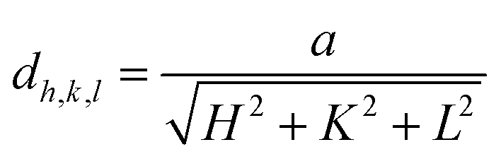
The microstructural, optical, and electrical properties of the produced In–Sm–O thin films with different Sm concentrations are summarized in Table 1. Fig. 1 shows the GIXRD patterns of these films. The broad peak at about 22.4° was attributed to the substrate. The peaks at 30.58°, 35.47°, 51.04°, and 60.68° corresponded well to the (222), (400), (440), and (622) diffraction peaks of the In2O3 crystal structure, respectively. In–Sm–O films with Sm doping below 5% showed a polycrystalline phase with (222) as the dominant peak. However, 10% Sm-doped In2O3 exhibited an amorphous phase, suggesting that too much Sm could frustrate In2O3 crystallization. The XRD results indicated that In–Sm–O with less than 5% Sm formed the same crystal structure as that formed by In2O3. The lattice constant of the cubic crystal In–Sm–O system was extracted using the formula35In this formula, dh,k,l denotes the interplanar spacing, a the lattice constant, and (HKL) the crystal face index. In this way, the lattice constants of 0, 2, 5% Sm doped In–Sm–O thin films were determined to be 10.080, 10.085, 10.092 Å, respectively. The obtained lattice constant of pristine In2O3 was found to be similar to the theoretical value (10.077 Å).28 The increase in the lattice constant with increasing amount of added Sm was attributed to the Sm3+ ionic radius (0.96 Å) being larger than the In3+ ionic radius (0.80 Å).28,31
| Sm concentration | Lattice constant (Å) | Grain size (nm) | RMS roughness (nm) | Optical bandgap (eV) | ρ (Ohm cm) | Carrier concentration (cm−3) | Hall mobility (cm2 V−1 s−1) |
|---|---|---|---|---|---|---|---|
| 0% | 10.080 | 11.50 | 0.177 | 3.35 | 0.364 | 3.55 × 10¹⁷ | 50.7 |
| 2% | 10.085 | 13.25 | 0.178 | 3.48 | 0.684 | 8.40 × 10¹⁶ | 44.8 |
| 5% | 10.092 | 16.09 | 0.216 | 3.61 | 11.9 | 1.90 × 10¹⁶ | 27.5 |
| 10% | Amorphous | Amorphous | 0.218 | 3.73 | 50.8 | 9.03 × 10¹⁵ | 13.5 |
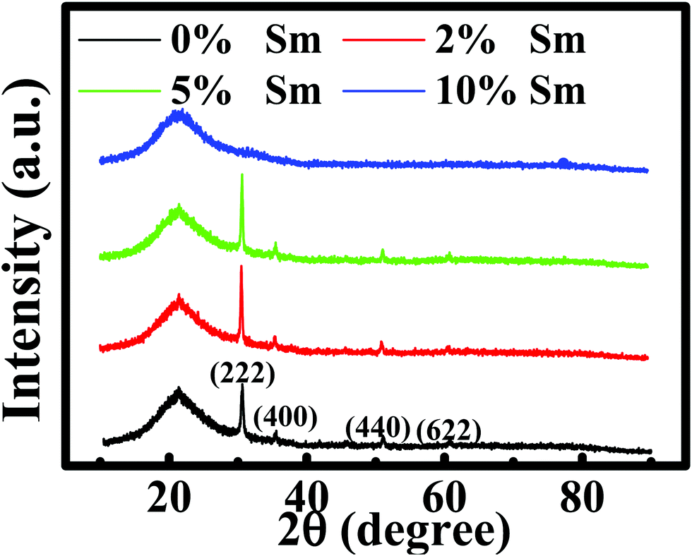 | ||
| Fig. 1 GIXRD patterns of the In–Sm–O thin films with various Sm contents. | ||
The grain sizes of the In–Sm–O thin films were calculated using the Scherer formula35
Fig. 2 displays the AFM images of In–Sm–O thin films with various Sm contents. The root mean square (RMS) roughness values of 0, 2, 5, and 10% Sm-doped In–Sm–O thin films were 0.177, 0.178, 0.216, 0.218 nm, respectively. These AFM results revealed all of the In–Sm–O films to be extremely smooth with an RMS on the average of 0.2 nm, indicated the Sm doping had little influence on the surface roughness, despite differences in crystallinity. Besides, the excellent surface roughness also indicated an absence of large grains or prominent grain boundaries in the crystalline In–Sm–O films, in line with the GIXRD analysis. Note that such an atomically smooth morphology is critical for achieving a high-performance TFT device, since it would minimize surface roughness scattering. The high quality and ultra-thin nature of the In–Sm–O (5% Sm) channel was further confirmed by acquiring a cross-sectional TEM image of it as shown in Fig. 3. The TEM image showed the In–Sm–O to be as thin as 5 nm, as well as extremely uniform and to have formed a continuous interface with SiO2 without pinholes. We also used XRR characterization to further confirm the thicknesses of the In–Sm–O thin films, as shown in Fig. S1 (ESI†) and summarized in Table S1 (ESI†). The In–Sm–O films with 0%, 2%, 5%, and 10% Sm contents were here measured to be 4.72 nm, 4.88 nm, 5.40 nm, and 5.84 nm, respectively. Therefore, the XRR results were in good agreement with the cross-sectional TEM measurements, confirming the thicknesses of the In–Sm–O films. The energy-dispersive X-ray spectroscopy (EDS) element distribution lines and mapping of elements are shown in Fig. S2 and S3 (ESI†), and a detailed analysis is provided in the ESI.† We were surprised to find that a nanometer-thick polycrystalline ternary oxide film with an atomically smooth topography could be grown from a simple aqueous solution.
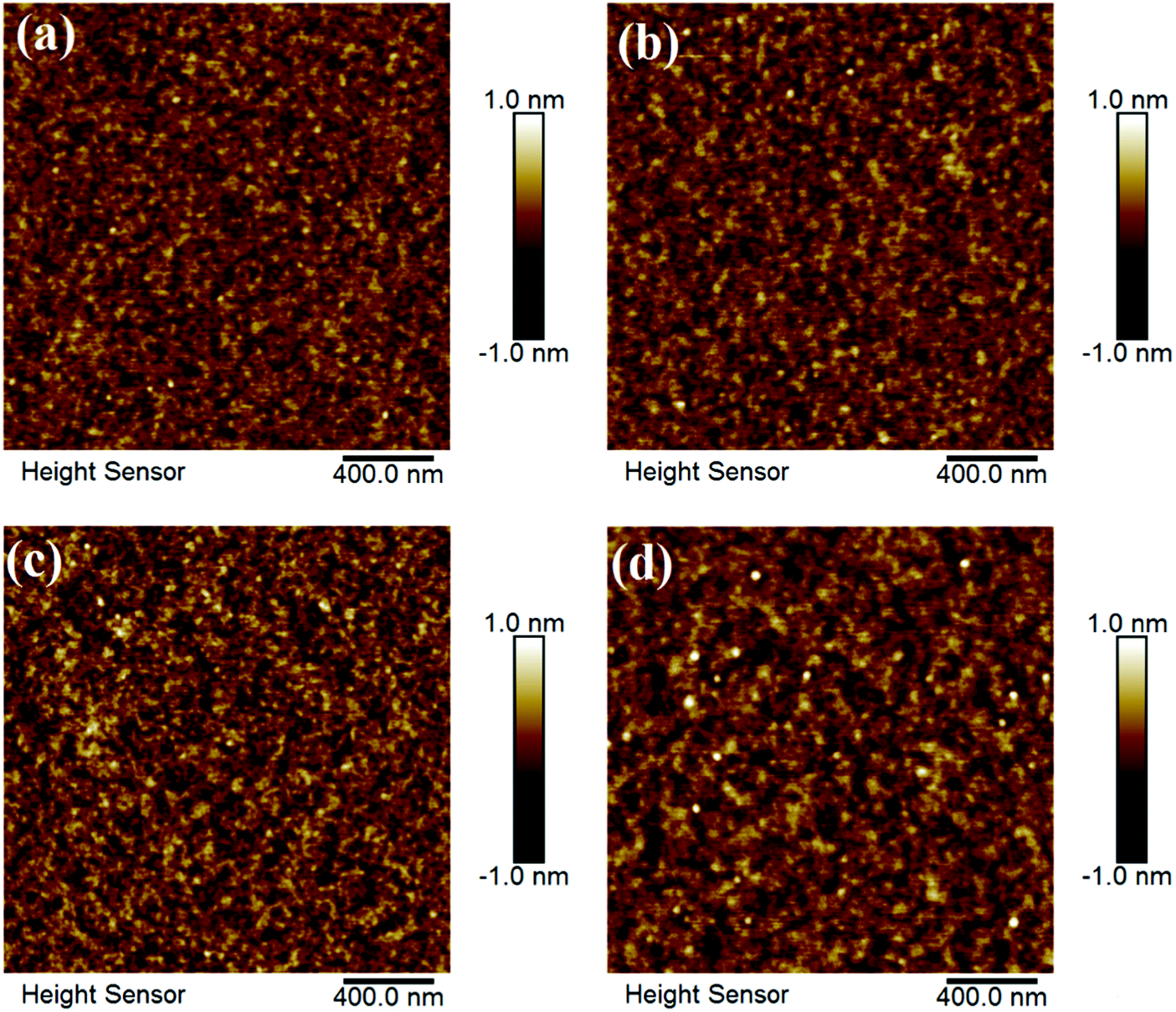 | ||
| Fig. 2 AFM images of the In–Sm–O thin films with various Sm contents: (a) 0%, (b) 2%, (c) 5%, and (d) 10%. | ||
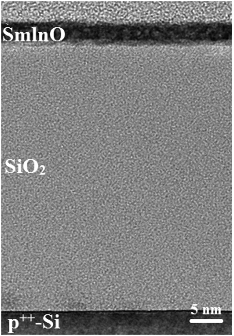 | ||
| Fig. 3 Cross-sectional TEM image of the In–Sm–O (5% Sm) thin film. | ||
Optical transmission spectroscopy was performed to investigate the influence of Sm doping on the optical bandgap (Eg) of the In–Sm–O thin film. As show in Fig. 4(a), the optical transmissions of all of the In–Sm–O thin films were over 85% between 400 nm and 800 nm, indicating great promise for their use in future transparent electronics. The Eg was calculated from the equation37
| (αhν)2 = C(hν − Eg). |
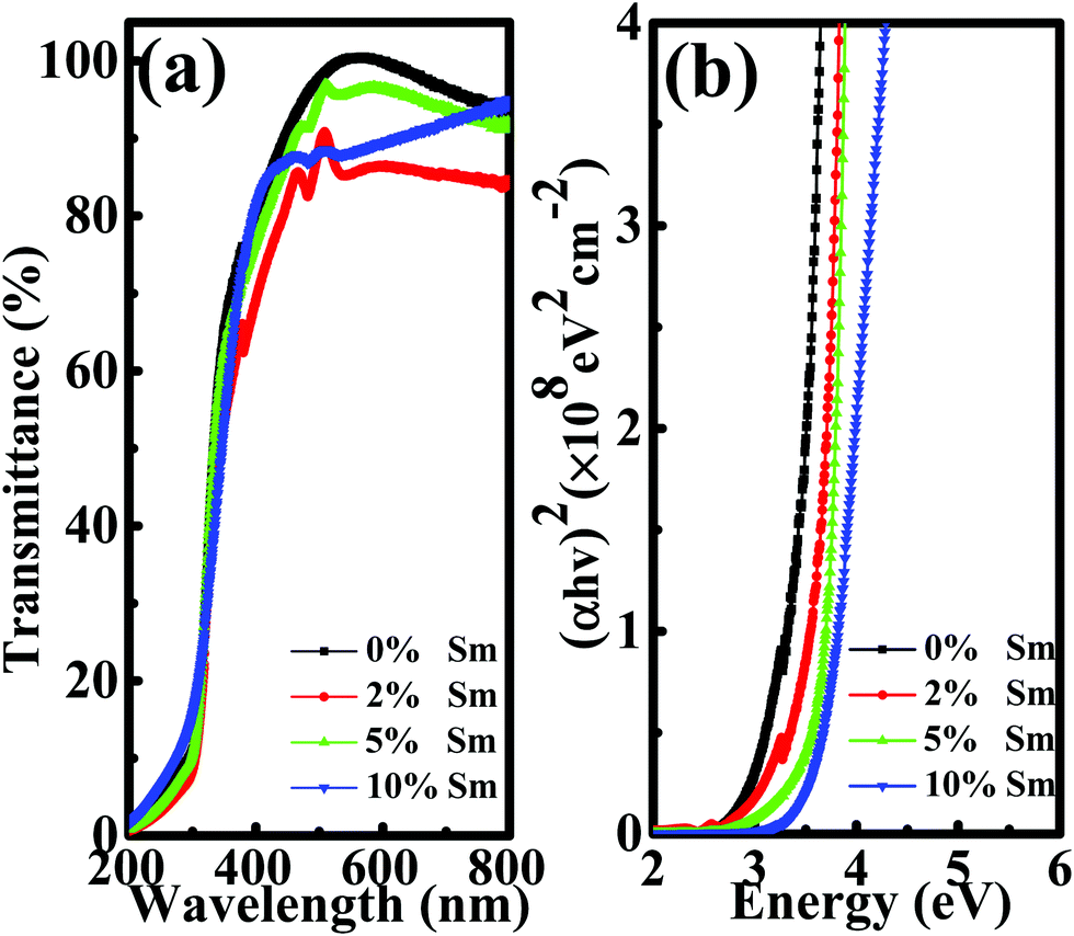 | ||
| Fig. 4 (a) Optical transmittance spectra and (b) obtained bandgaps of In–Sm–O thin films with different Sm contents. | ||
Fig. 5 shows PL spectra of In–Sm–O thin films with various Sm contents. Fig. 5(a) specifically shows the spectra each spanning wavelengths from about 350 to 750 nm, whereas Fig. 5(b) and (c) show normalized PL spectra in the vicinities of the observed ∼600 and ∼420 nm peaks, respectively. Compared to the ∼600 nm peak, that at ∼420 nm was relatively weak and was related to the near-band-edge (NBE) emission.38 The ∼600 nm peak was attributed to the recombination between a shallow donor near the conduction band minimum (CBM) and acceptors (neutral oxygen vacancies) trapped above the valence band maximum (VBM).39 So the major peak could be ascribed to oxygen vacancies. The PL peak intensity decreased with increasing Sm incorporation, indicating that Sm acted as an effective oxygen vacancy suppressor.
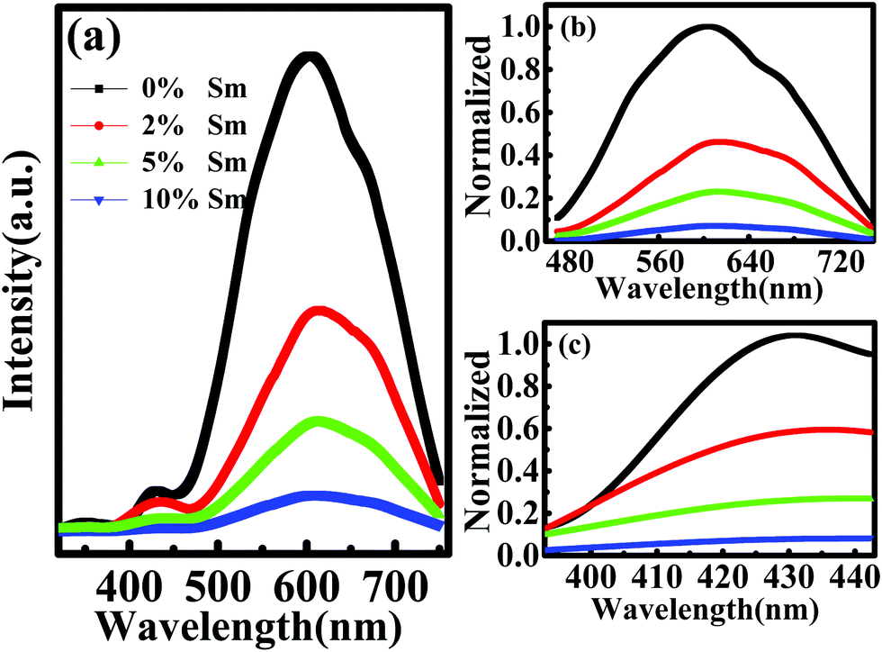 | ||
| Fig. 5 PL spectra of In–Sm–O thin films with various Sm contents. (a) Spectra spanning wavelengths from about 350 to 750 nm. (b and c) Normalized PL spectra in the vicinities of the observed ∼600 and ∼420 nm peaks. | ||
XPS was carried out to investigate the chemical states of the In–Sm–O films. Fig. 6(a) and Table 2 show features of the O 1s peak for each film. The peak could be divided into three subpeaks centered at 529.64–529.68 eV (OM), 530.50–530.56 eV (OV), 531.49–531.86 eV (OH). The OM, OV, and OH peaks were related to oxygen in oxide lattices (M–O–M), oxygen vacancies (VO), and metal hydroxide species (M–OH), respectively. The OM/(OM + OV + OH) ratio increased after introduction of Sm, indicating that the addition of Sm promoted the formation of the metal oxide lattice. As the Sm concentration was increased from 0 to 10%, the OV/(OM + OV + OH) ratio fell from 26.25 to 5.29%. This result indicated the excellent ability of the Sm3+ ion to suppress the formation of oxygen vacancies, attributed to a stronger bonding of Sm than of In to O, i.e., attributed to Sm–O and In–O bond strengths of 573 kJ mol−1 and 346 kJ mol−1, respectively.31,40 Besides, the increased OH/(OM + OV + OH) ratio with excess Sm (10%) indicated an incomplete dehydration of residual Sm(OH)3.41Fig. 6(b) and (c) show the XPS spectra in the regions of the In 3d and Sm 3d peaks for In–Sm–O with different Sm doping contents The In XPS peaks shifted toward lower binding energy with increased Sm doping, revealing again the stronger bonding of Sm than of In to O. The signal at the Sm 3d binding energy of 1075–1085 eV was assigned to Sm3+ ion, indicating the formation of Sm–O bonding.42
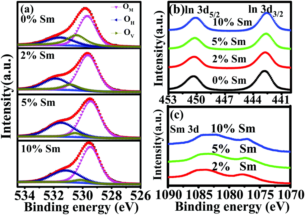 | ||
| Fig. 6 XPS spectra in the (a) O 1s, (b) In 3d, and (c) Sm 3d regions for In–Sm–O thin films with different Sm doping contents. | ||
| Sm concentration | 0% | 2% | 5% | 10% |
|---|---|---|---|---|
| OM position (eV) | 529.67 | 529.68 | 529.64 | 529.66 |
| FWHM | 1.41 | 1.51 | 1.58 | 1.53 |
| Area | 75237.82 | 87232.85 | 87456.27 | 92721.54 |
| Ov position (eV) | 530.51 | 530.56 | 530.50 | 530.53 |
| FWHM | 1.57 | 1.34 | 1.11 | 1.22 |
| Area | 37375.02 | 14349.66 | 8704.59 | 7426.23 |
| OH position (eV) | 531.55 | 531.86 | 531.49 | 531.66 |
| FWHM | 2.16 | 1.99 | 2.16 | 2.25 |
| Area | 29754.21 | 33962.02 | 46290.81 | 40254.67 |
| OM/(OM + OV + OH) | 52.85% | 64.36% | 65.94% | 66.04% |
| OV/(OM + OV + OH) | 26.25% | 10.68% | 6.11% | 5.29% |
| OH/(OM + OV + OH) | 20.90% | 25.06% | 27.95% | 28.67% |
Hall effect measurements were taken to examine the electrical properties of the In–Sm–O films. The resistivity, carrier concentration, and Hall mobility levels of the In–Sm–O films with different relative amounts of Sm are summarized in Table 1. As the Sm doping content was increased from 0 to 10%, the resistivity of In–Sm–O increased from 0.346 to 50.8 Ohm cm, the carrier concentration decreased from 3.55 × 10¹⁷ to 9.03 × 1015 cm−3, and the Hall mobility fell from 50.7 to 13.5 cm2 V−1 s−1. Oxygen vacancies are generally considered to be the electron donors in oxide semiconductors. Therefore, the reduction in carrier concentration after Sm incorporation was attributed to the suppression of oxygen vacancies. However, the incorporation of Sm would reduce the overlap of In 5s orbitals, and hence reduce the mobility.28 The Hall results suggested an excellent ability of the Sm dopant to suppress the oxygen vacancies and control the electron concentration, in good agreement with the PL and XPS analyses.
Fig. 7 displays the representative transfer (VDS = 20 V) and output characteristics for the In–Sm–O TFTs with different amounts of doped Sm using 100 nm SiO2 as a gate dielectric. The leakage currents of the SiO2 samples are shown in Fig. S4 (ESI†). The averages of the values of each of various electrical parameters (μ, Vth, Ion/Ioff, and SS) taken from at least In–Sm–O 15 TFTs of each amount of Sm doped and the distributions of these values are summarized in Table 3 and Fig. 8. Note that pristine In2O3 TFTs prepared using the simple aqueous route showed high electron mobility, exceeding 30 cm2 V−1 s−1, but suffered from a high Ioff (∼10−7 A) and large negative Vth (−7.16 V), attributed to the overly high carrier concentration. Although high mobility is important for a high-speed operation, controlling Ioff and Vth is also critical for saving energy. As the Sm doping content was increased from 0 to 10%, the Ioff fell from 10−7 to ∼10−11 A and Vth shifted from −7.16 to 3.21 V. The enhancement of Ioff and Vth after the incorporation of Sm was attributed to the reduction of carrier concentration via suppressed oxygen vacancies. Meanwhile, the average mobility for the In–Sm–O TFTs decreased from 30.64 to 5.16 cm2 V−1 s−1 as the Sm content was increased from 0 to 10%, which was attributed to the reduced overlap of In 5s orbitals. This TFT performance trend was in good agreement with the results of the Hall effect measurements. Note that device mobility was lower than the Hall mobility, which was attributed to the dielectric/semiconductor interface scattering. Additionally, the SS value also improved from 2.65 to 0.55 V per decade as the Sm content was increased from 0 to 10%. Generally, the SS value is the indicator of active layer or active layer/dielectric interface trap density (Nt). The Nt in our In–Sm–O TFTs was calculated to decline from 8.58 × 10¹² to 1.78 × 1012 cm−2 eV−1 as the Sm doping was increased. This decline was attributed to Sm doping suppressing the formation of oxygen vacancies, leading to the reduction of trap states in the In–Sm–O TFTs, in line with the improvement in Ion/Ioff and Vth. A detailed discussion of the changes in electrical parameters after Sm doping is provided in the ESI.†
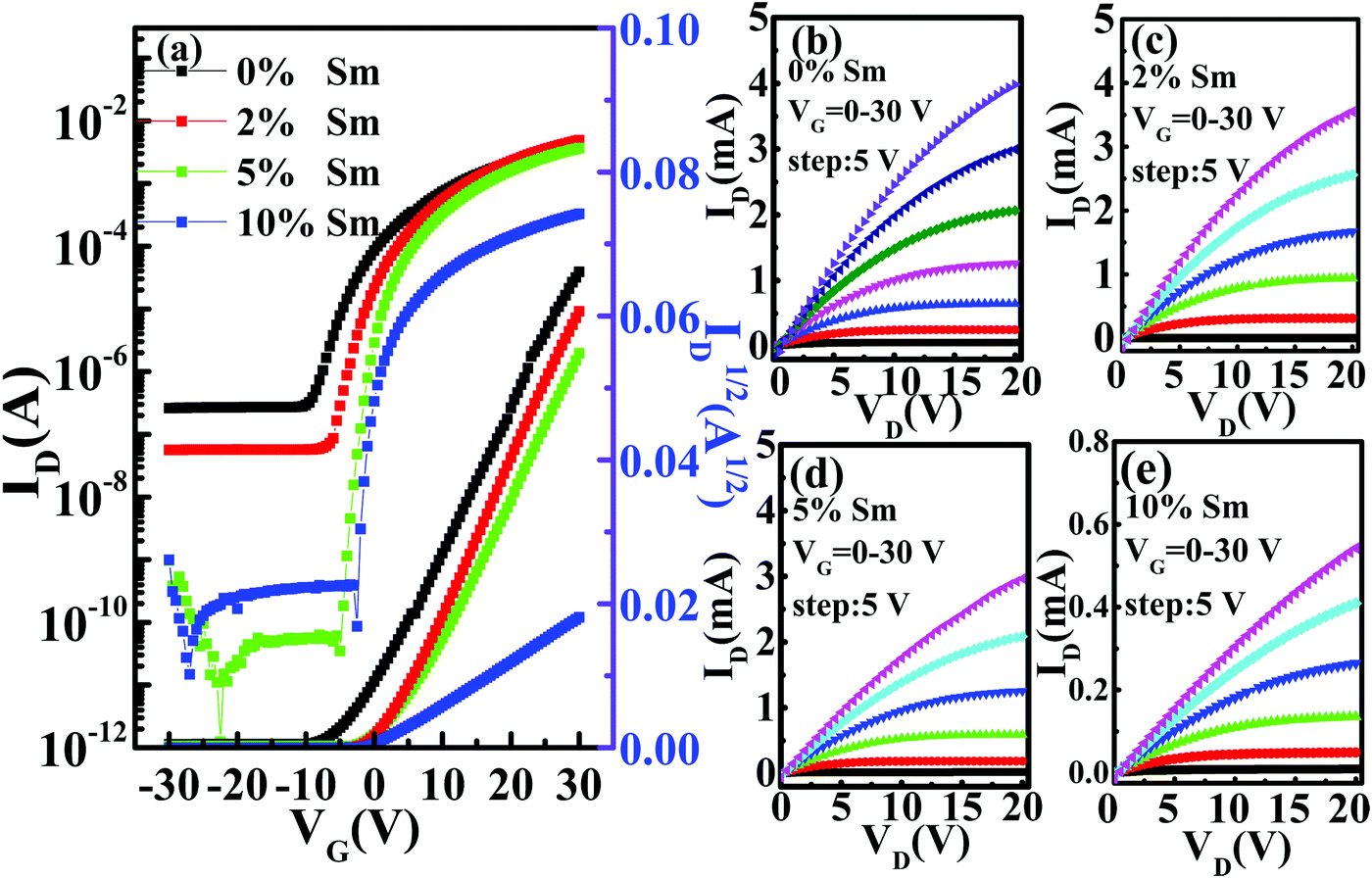 | ||
| Fig. 7 (a) Transfer and (b–e) output characteristics of the In–Sm–O TFTs with various Sm contents. | ||
| Sm concentration (%) | μ (cm2 V−1 s−1) | I on/Ioff | SS (V dec−1) | V th (V) | N t (cm−2 eV−1) |
|---|---|---|---|---|---|
| 0 | 30.64 ± 2.54 | 1.74 × 10⁴ | 2.65 ± 0.12 | −7.16 ± 0.56 | 8.58 × 10¹² |
| 2 | 24.43 ± 1.84 | 4.26 × 10⁴ | 1.26 ± 0.08 | −3.06 ± 0.34 | 4.08 × 10¹² |
| 5 | 21.51 ± 1.33 | 1.09 × 10⁸ | 0.66 ± 0.06 | 2.14 ± 0.44 | 2.14 × 10¹² |
| 10 | 5.16 ± 0.96 | 1.89 × 10⁵ | 0.55 ± 0.15 | 3.21 ± 0.54 | 1.78 × 10¹² |
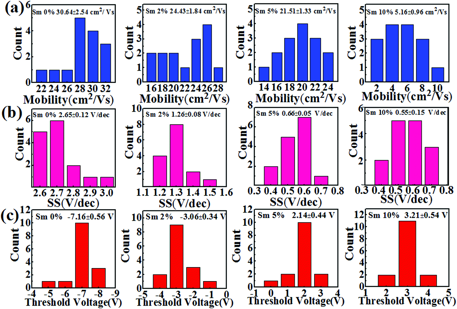 | ||
| Fig. 8 (a) Mobility, (b) subthreshold swing, and (c) threshold voltage histograms for the In–Sm–O TFTs with various Sm contents. The data for each Sm content were collected from 15 TFTs. | ||
The optimized In–Sm–O (5% Sm) TFTs exhibited a striking electrical performance, including a high μ of 21.51 ± 1.33 cm2 V−1 s−1, excellent Ion/Ioff of up to 1.09 × 10⁸, SS of 0.66 ± 0.06 V per decade, and Vth of 2.14 ± 0.44 V. The transfer curves in the linear regime (VDS = 0.5 V) for In–Sm–O TFTs are shown in Fig. S5 (ESI†), with the linear mobility summarized in Table S2 (ESI†). The linear mobility was in good agreement with the saturation mobility. Besides, the electrical characteristics of the lower-temperature annealing (250 °C) for In–Sm–O TFTs are shown in Fig. S6 (ESI†) and summarized in Table S3 (ESI†), and a detailed analysis is provided in the ESI.†Table 4 summarizes the recent developments in solution-processed ternary and quaternary oxide TFTs. To provide a high-quality comparison, publications were selected based on the Si/SiO2 substrate/dielectric since the use of a high-K dielectric often leads to an overestimation of device mobility.3 Our ultra-thin In–Sm–O transistors demonstrated state-of-the-art performance. Besides, due to In–Sm–O channel having been grown using simple one-step spin coating of an aqueous precursor accompanied with a moderate annealing temperature, our procedure holds great promise for future low-cost large-area green electronics. Additionally, since the Young's modulus is inversely proportional to film thickness, the ultra-thin nature of the In–Sm–O channel would allow it to endure high mechanical strain for flexible electronics.43
| Channel | Processing temperature (°C) | Mobility (cm2 V−1 s−1) | I on/Ioff | SS | Year | Ref. |
|---|---|---|---|---|---|---|
| In–Al–O | 300 | 0.21 | 107 | 0.50 | 2013 | 25 |
| In–La–Zn–O | 300 | 1.81 | 107 | — | 2013 | 17 |
| In–Y–Zn–O | 300 | 2.37 | 107 | — | 2013 | 17 |
| In–Sc–Zn–O | 300 | 2.57 | 108 | — | 2013 | 17 |
| In–Ba–Zn–O | 450 | 17.18 | 108 | — | 2014 | 26 |
| In–Sr–Zn–O | 450 | 25 | 108 | — | 2014 | 26 |
| In–Zn–O | 350 | 13.0 | 108 | 0.41 | 2014 | 18 |
| In–S–Zn–O | 350 | 8.1 | 108 | 0.30 | 2014 | 18 |
| In–P–Zn–O | 350 | 6.3 | 107 | 0.42 | 2014 | 18 |
| In–Ga–Zn–O | 300 | 6.8 | 106 | — | 2015 | 19 |
| In–B–Zn–O | 500 | 10.15 | 108 | 0.35 | 2016 | 20 |
| In–Sb–O | 300 | 4.6 | 107 | 0.29 | 2017 | 21 |
| In–Mg–O | 500 | 13.7 | 107 | 0.55 | 2017 | 14 |
| In–B–O | 300 | 11.3 | 105 | 0.17 | 2018 | 16 |
| In–Ga–Cd–O | 400 | 10 | 109 | — | 2018 | 22 |
| In–Ga–O | 350 | 0.5 | 106 | 0.45 | 2018 | 13 |
| In–Y–O | 350 | 0.4 | 106 | 0.45 | 2018 | 13 |
| In–Mg–Zn–O | 400 | 1.97 | 107 | 0.69 | 2019 | 15 |
| In–Si–O | 800 | 0.21 | 107 | 0.50 | 2019 | 30 |
| In–Sm–O | 350 | 21.51 | 108 | 0.55 | Our work | Our work |
Several reasons for the success of the In–Sm–O TFTs were identified. First, the high mobility for the In–Sm–O channel originated from the high quality of the crystalline In2O3. Previous studies showed a much higher mobility for crystalline In2O3 than for amorphous In2O3, attributed to disorder within the film resulting in a smaller overlap of the In 5s orbitals and thus low electron mobility.44 In our current study, by carefully optimizing the precursor concentration and post annealing temperature, high-quality nanocrystalline In2O3 with an extremely smooth surface (observed using GIXRD, AFM, and TEM) was realized with a Hall mobility (50.7 cm2 V−1 s−1) and field effect mobility (30.6 cm2 V−1 s−1) comparable to those of its vapor-deposited counterpart.43 Secondly, although pristine In2O3 showed a high mobility, its Ioff, Vth, and SS values were poor, attributed to excessive oxygen vacancies. Therefore, incorporating a suitable dopant is indispensable to suppress oxygen vacancies and enhance the device performance. Previous research suggested that a dopant with a low SEP, low electronegativity, and high bonding strength with oxygen could effectively suppress oxygen vacancies. Sm has a low SEP of −2.30 V, low electronegativity of 1.17, and strong oxygen-bonding strength of 573 kJ mol−1.31,42 Furthermore, Sm3+ has the same valence state as does In3+, and hence the Sm3+ would not generate additional carriers.23 Consequently, the addition of Sm apparently effectively reduced the carrier concentration in our In2O3 samples due to the suppression of oxygen vacancies (confirmed using XPS and PL), leading to improvements of Ioff, Vth, and SS values. As a strong oxygen binder, a small amount of added Sm (5%) apparently successfully suppressed oxygen vacancies, thus minimizing impurity scattering and resulting in an In–Sm–O displaying high charge mobility, specifically a Hall mobility of 27.5 cm2 V−1 s−1, and field effect mobility of 21.51 ± 1.33 cm2 V−1 s−1. Meanwhile, Sm2O3 and ln2O3 form the same bixbyite structure, which could lead to low defect states.33,34 Although the mobility for In–Sm–O (5%) was lower than that for pristine In2O3, it was still sufficient for high-performance TFT applications. Thirdly, the high performance of the In–Sm–O TFTs was also related to the ultrathin nature of In–Sm–O, which contained fewer defect states in the channel material compared with a thicker film. More importantly, for solution processing in general, large amounts of gases evolve during post-annealing, and hence an oxide thin film must be sufficiently thin to maintain continuity and densification without porosity.19 Note that nanoporous structures in oxide thin films usually act as defect states, deteriorating device performance. Besides, atomically smooth channel/dielectric interfaces also generally support pathways amenable to ultra-fast electron transport. Fig. S7 (ESI†) displays the electrical properties for In–Sm–O TFTs with different thicknesses, and their electrical characteristics are summarized in Table S3 (ESI†). In–Sm–O TFTs with a thickness of ∼5 nm demonstrated the best performance, and a detailed analysis is shown in the ESI.† Fourthly, the high performance of In–Sm–O was also attributed to the aqueous solution processing. Water has been shown to be an excellent solvent for such cases since it does not contain organic residues that would otherwise need to be removed.45 In addition, nitrated salts in water usually form a hexaaqua structure M(H2O)6 (with M in our case being In or Sm), which is easily broken with a low energy supply.45 Thus, an In–Sm–O film with a dense and smooth nature was achieved at a low annealing temperature. Solution processing also enables the modulation of oxide composition easily by changing the precursor composition. These factors were concluded to synergistically contribute to the high performance of the solution-based In–Sm–O TFTs.
To evaluate the stability levels of the In–Sm–O TFTs, the devices were subjected to positive bias stress (PBS, VG = 20 V) or negative bias stress (NBS, VG = −20 V) under ambient conditions. Fig. 9(a) shows the transfer curves for In–Sm–O TFTs with different relative amounts of Sm in PBS and subjected to stress conditions for up to 30 minutes with 5 minute intervals. The Vth values of the In–Sm–O devices gradually shifted to the positive direction with increasing duration of applied stress. The positive Vth shift was ascribed to the charge trapping at the In–Sm–O channel or channel/dielectric interface.3 Besides, since our devices were not passivated, the adsorption of oxygen molecules also contributed to the Vth shift.3 Note that as the Sm doping content was increased from 0 to 5%, a significant reduction of the Vth shift (from 11.5 V to 2.5 V) was observed, a result related to the suppression of oxygen vacancies. However, 10% Sm doping decreased the PBS stability. This result may be attributed to the increase in the number of defects caused by structural disorder as shown using GIXRD.23 Besides, Sm is a rare earth element, whose 4f electrons have several split states, which may act as trap states and decrease PBS stability. Ioff decreased with bias stress time for 0% or 2% Sm-doped In–Sm–O TFTs, due to the reduction of conductivity after bias, a detailed analysis of which is provided in the ESI.†
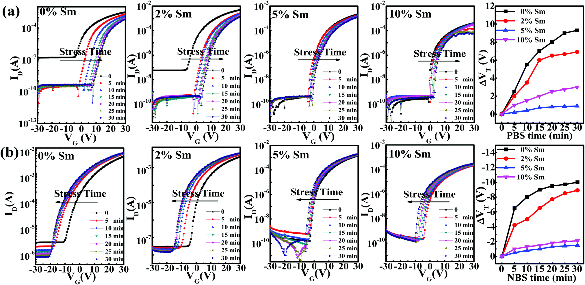 | ||
| Fig. 9 (a) Transfer curves for various In–Sm–O TFTs under different stress times with (a) PBS (VG = 20 V) and (b) NBS (VG = −20 V). | ||
The NBS stability of In–Sm–O TFTs with different Sm contents was also investigated, and the results are shown in Fig. 9(b). The In–Sm–O transistors showed negative Vth shifts under NBS stress. A negative Vth shift is generally attributed to the release of electrons from donor-like traps, also associated with oxygen vacancies.46 And the Vth shift in the current experiments was found to improve from 12.5 V to 3 V as the relative amount of Sm added was increased from 0 to 5%. However, the NBS stability then decreased as the Sm doping content was increased further to 10%, a result also related to structural disorder defects. The decline in crystallinity for higher Sm dopings inevitably induced the formation of more defect states and resulted in poor electrical stability. Additionally, the split states of Sm 4f electrons could have also contributed to the NBS stability. Overall, the In–Sm–O TFTs with a 5% Sm doping content exhibited the optimal bias stress stability along with high electrical performance.
4. Conclusions
In summary, we grew nanometer-thick crystalline In–Sm–O films from an aqueous route. It was revealed that appropriate Sm doping could effectively reduce excess carrier concentration by suppressing oxygen vacancies. By optimizing the relative amount of Sm doped, In–Sm–O TFTs on thermal SiO2 dielectrics demonstrated a mobility value exceeding 21 cm2 V−1 s−1 with an on/off current ratio higher than 108 and superior bias stress stability. The high performance of the transistors could be attributed to the high quality of the crystalline In2O3 matrix, the ideal nature of using Sm as a dopant to suppress oxygen vacancies, and the ultrathin and atomically smooth nature of the In–Sm–O films. Thus, the ultra-thin In–Sm–O channel is considered to be a promising candidate for next-generation, low-cost high-performance printed electronics.Conflicts of interest
There are no conflicts to declare.Acknowledgements
We thank the National Natural Science Foundation of China (61704111, 51872187, 51371120 and 11774241), Natural Science Foundation of Guangdong Province (2017A030310524), and Science and Technology Foundation of Shenzhen (JCYJ20170817100611468 and JCYJ20170818143417082) for their great support.References
- X. Yu, T. J. Marks and A. Facchetti, Nat. Mater., 2016, 15, 383 CrossRef CAS.
- E. Fortunato, P. Barquinha and R. Martins, Adv. Mater., 2012, 24, 2945–2986 CrossRef CAS.
- W. Xu, H. Li, J.-B. Xu and L. Wang, ACS Appl. Mater. Interfaces, 2018, 10, 25878–25901 CrossRef CAS.
- L. L. Zheng, S. B. Qian, Y. H. Wang, W. J. Liu and S. J. Ding, IEEE J. Electron Devices Soc., 2016, 4, 1 Search PubMed.
- G. Z. Geng, G. X. Liu, F. K. Shan, A. Liu, Q. Zhang, W. J. Lee, B. C. Shin and H. Z. Wu, Curr. Appl. Phys., 2014, 14, S2–S6 CrossRef.
- C. Glynn and C. O'Dwyer, Adv. Mater. Interfaces, 2017, 4, 1600610 CrossRef.
- K. K. Banger, Y. Yamashita, K. Mori, R. L. Peterson, T. Leedham, J. Rickard and H. Sirringhaus, Nat. Mater., 2011, 10, 45–50 CrossRef CAS.
- S. Jeong and J. Moon, J. Mater. Chem., 2011, 22, 1243–1250 RSC.
- R. M. Pasquarelli, D. S. Ginley and O. H. Ryan, Chem. Soc. Rev., 2015, 43, 5406–5441 Search PubMed.
- A. Liu, G. Liu, H. Zhu, Y. Meng, H. Song, B. Shin, E. Fortunato, R. Martins and F. Shan, Curr. Appl. Phys., 2015, 15, S75–S81 CrossRef.
- R. Chen and L. Lan, Nanotechnology, 2019, 30, 312001 CrossRef.
- R. E. Presley, C. L. Munsee, C. H. Park, D. Hong, J. F. Wager and D. A. Keszler, J. Phys. D: Appl. Phys., 2004, 37, 2810 CrossRef CAS.
- F. Jaehnike, D. V. Pham, C. Bock and U. Kunze, J. Mater. Chem. C, 2019, 7, 7627–7635 RSC.
- C. Y. Zhao, J. Li, D. Y. Zhong, C. X. Huang, J. H. Zhang, X. F. Li, X. Y. Jiang and Z. L. Zhang, IEEE Trans. Electron Devices, 2017, 64, 2216 CAS.
- J. Cheng, X. Y. Li, J. Guo, H. F. Xu, Y. H. Chen, Y. F. He, J. S. Xue, T. Zhang and Z. N. Yu, J. Alloys Compd., 2019, 793, 369–374 CrossRef CAS.
- X. Zhang, B. Wang, W. Huang, Y. Chen, G. Wang, L. Zeng, W. Zhu, M. J. Bedzyk, W. Zhang, J. E. Medvedeva, A. Facchetti and T. J. Marks, J. Am. Chem. Soc., 2018, 140, 12501–12510 CrossRef CAS.
- J. W. Hennek, S. Jeremy, Y. Aiming, K. Myung-Gil, Z. Wei, V. P. Dravid, F. Antonio and T. J. Marks, J. Am. Chem. Soc., 2013, 135, 10729–10741 CrossRef CAS.
- H. Park, Y. Y. Nam, J. Jin and B. S. Bae, J. Mater. Chem. C, 2014, 2, 5998 RSC.
- X. Yu, J. Smith, N. Zhou, L. Zeng, P. Guo, Y. Xia, A. Alvarez, S. Aghion, H. Lin, J. Yu, R. P. H. Chang, M. J. Bedzyk, R. Ferragut, T. J. Marks and A. Facchetti, Proc. Natl. Acad. Sci. U. S. A., 2015, 112, 3217–3222 CrossRef CAS.
- D. Y. Zhong, J. Li, C. Y. Zhao, C. X. Huang, J. H. Zhang, X. F. Li, X. Y. Jiang and Z. L. Zhang, IEEE Trans. Electron Devices, 2017, 1–6 Search PubMed.
- T. Kim, B. Jang, J. H. Bae, H. Park, C. S. Cho, H. J. Kwon and J. Jang, IEEE Electron Device Lett., 2017, 38, 1027 Search PubMed.
- A. Song, K. Javaid, L. Yu, W. Wu, J. Yu, L. Liang, H. Zhang, L. Lan, T. C. Chang and H. Cao, Phys. Status Solidi RRL, 2018, 12 Search PubMed.
- Z. Lin, L. Lan, S. Sun, Y. Li, W. Song, P. Gao, E. Song, P. Zhang, M. Li, L. Wang and J. Peng, Appl. Phys. Lett., 2017, 110, 133502 CrossRef.
- J. Smith, L. Zeng, R. Khanal, K. Stallings, A. Facchetti, J. E. Medvedeva, M. J. Bedzyk and T. J. Marks, Adv. Electron. Mater., 2015, 1, 11–16 Search PubMed.
- Y. H. Hwang and B. S. Bae, J. Disp. Technol., 2013, 9, 704–709 CAS.
- K. K. Banger, R. L. Peterson, K. Mori, Y. Yamashita, T. Leedham and H. Sirringhaus, Chem. Mater., 2014, 26, 1195–1203 CrossRef CAS.
- C.-Y. Zhao, J. Li, D.-Y. Zhong, C.-X. Huang, J.-H. Zhang, X.-F. Li, X.-Y. Jiang and Z.-L. Zhang, IEEE Trans. Electron Devices, 2017, 65, 1–7 Search PubMed.
- S. H. Lee, T. Kim, J. Lee, C. Avis and J. Jang, Appl. Phys. Lett., 2017, 110, 122102 CrossRef.
- Z. Lin, L. Lan, X. Peng, S. Sheng, Y. Li, S. Wei, P. Gao, E. Song, Z. Peng and W. Lei, IEEE Electron Device Lett., 2016, 37, 1139–1142 CAS.
- H. Hoang, T. Hori, T.-O. Yasuda, T. Kizu, K. Tsukagoshi, T. Nabatame, B. Trinh and A. Fujiwara, Mater. Res. Exp., 2018, 6, 039601 CrossRef.
- A. A. Dakhel, J. Alloys Compd., 2004, 365, 233–239 CrossRef CAS.
- C. L. Deasy, J. Chem. Educ., 1941, 18, 514 CrossRef CAS.
- Z. Lin, L. Lan, X. Peng, S. Sheng, Y. Li, S. Wei, P. Gao and J. Peng, Appl. Phys. Lett., 2014, 105, 913 Search PubMed.
- M. V. Abrashev, N. D. Todorov and J. Geshev, J. Appl. Phys., 2014, 116, 367 CrossRef.
- Y. Li, W. Xu, W. Liu, S. Han, P. Cao, M. Fang, D. Zhu and Y. Lu, ACS Appl. Electron. Mater., 2019, 1, 1842–1851 CrossRef CAS.
- C. C. Ting, H. Y. Fan, M. K. Tsai, W. Y. Li, H. E. Yong and Y. F. Lin, Phys. Status Solidi A, 2014, 211, 800 CrossRef CAS.
- M. Benwadih, J. A. Chroboczek, G. Ghibaudo, R. Coppard and D. Vuillaume, J. Appl. Phys., 2014, 115, 013502 CrossRef.
- W. Xu, L. Hu, C. Zhao, L. Zhang, D. Zhu, P. Cao, W. Liu, S. Han, X. Liu, F. Jia, Y. Zeng and Y. Lu, Appl. Surf. Sci., 2018, 455, 554 CrossRef CAS.
- J. Jia, A. Suko, Y. Shigesato, T. Okajima, K. Inoue and H. Hosomi, Phys. Rev. Appl., 2018, 9, 014018 CrossRef CAS.
- S. Parthiban and J. Y. Kwon, J. Mater. Res., 2014, 29, 1585 CrossRef CAS.
- X. Zhang, B. Wang, W. Huang, Y. Chen, G. Wang, L. Zeng, W. Zhu, M. J. Bedzyk, W. Zhang, J. E. Medvedeva, A. Facchetti and T. J. Marks, J. Am. Chem. Soc., 2018, 140, 12501 CrossRef CAS.
- D. Briggs, Handbook of x-ray and ultraviolet photoelectron spectroscopy, 1978 Search PubMed.
- J. Lee, J. Moon, J. E. Pi, S. D. Ahn and K. H. Kwon, Appl. Phys. Lett., 2018, 113, 112102 CrossRef.
- D. B. Buchholz, Q. Ma, D. Alducin, A. Ponce, M. Jose-Yacaman, R. Khanal, J. E. Medvedeva and R. P. Chang, Chem. Mater., 2014, 26, 5401–5411 CrossRef CAS.
- Y. H. Hwang, J. S. Seo, J. M. Yun, H. J. Park, S. Yang, S. H. K. Park and B. S. Bae, NPG Asia Mater., 2013, 5, e45 CrossRef CAS.
- H. J. Jeong, K. C. Ok, J. Park, J. Lim and J. S. Park, IEEE Electron Device Lett., 2015, 36, 1160–1162 CAS.
Footnote |
| † Electronic supplementary information (ESI) available. See DOI: 10.1039/c9tc05162g |
| This journal is © The Royal Society of Chemistry 2020 |