Fabrication of indium gallium zinc oxide phototransistors via oxide-mesh insertion for visible light detection†
Received
9th September 2019
, Accepted 13th November 2019
First published on 15th November 2019
Abstract
We developed amorphous indium gallium zinc oxide (a-IGZO) phototransistors that could sense up to the red light region of the visible light spectrum. The vital element of the utilized technology in this study is the creation of defects within the a-IGZO thin film that serves as the channel layer of a thin film transistor (TFT) through structural engineering. The defects are induced by inserting mesh-structured titanium dioxide (m-TiO2) layers inside the channel. The oxygen vacancies thus generated create subgap states within the band gap of a-IGZO, enabling detection of the visible light with wide wavelengths. As a result, the optimized a-IGZO phototransistor with m-TiO2 inserted inside the channel layer exhibited a photoresponsivity of 178.66 A W−1, a photosensitivity of 1.04 × 10⁵, and a detectivity of 1.25 × 10¹⁰ Jones under monochromatic red light (635 nm wavelength) illumination.
Introduction
As technology advances, various machines facilitating daily tasks and recreational activities have exploded in number as people demand for a more comfortable life. Once people have tasted the comfort offered by these machines, their insatiable hunger for more has hastened further advances. As such, various electronics such as smart homes and autonomous vehicles are in development to offer direct interaction with various consumer electronics, home appliances, and even vehicles for more comfortable living. However, in order to realize such technology, all interlinked appliances must be able to sense the environment. For that purpose, various types of sensors are in extensive research for integration into these appliances. Among various types of sensors, photosensors are essential in this regard as they enable the detection of the environment through the change or presence of light. Therefore, photosensors are in extensive research and development for diverse applications such as vehicles, mobile devices, televisions, medical devices, and robots.1–4
Presently, among various types of photosensors, thin-film transistor (TFT)-based photosensors, i.e., phototransistors, using amorphous oxide semiconductors (AOSs) as the channel layers are exceptionally promising as they have wavelength- and intensity-selectivity in terms of the incident light. This is because the AOSs that are used as the channel layers usually have a wide band gap of around 3.0 eV and subgap states within. When the incident light has much lower energy than the band gap energy, the light is absorbed only by electrons trapped at subgap states within the band gap. As the intensity of the light increases, more photons are emitted. Therefore, an increased number of photons are absorbed by more electrons trapped at subgap states and the drain current (ID) increases accordingly. Similarly, as the wavelength of the incident light decreases, the light energy increases, and thus photons penetrate further into the band gap. This excites more electrons from the subgap states that lie further within the band gap, so this increases ID accordingly.5
Additionally, AOS-based TFTs exhibit high uniformity over large area similar to amorphous silicon (a-Si), higher field-effect mobility (μFE) than a-Si-based TFTs, and lower off-current (Ioff) than low-temperature poly-silicon (LTPS)-based TFTs. Therefore, many researchers have made efforts to further enhance the performance of AOS-based TFTs alone.6–10 However, due to the band gap of around 3.0 eV, AOSs have high transparency. Thus, they cannot readily absorb visible light with wide wavelength as the energy of the visible light ranges from 1.7 to 3.1 eV (700 to 400 nm in wavelengths). As one of the widely used AOSs, amorphous indium gallium zinc oxide (a-IGZO) also has this characteristic with a band gap greater than 3.0 eV. Thus, a-IGZO-based phototransistors are usually used to detect ultraviolet (UV) or blue light with energy greater than 3.0 eV.11–14 Therefore, there are many research studies to enable a-IGZO phototransistors to detect visible light of wavelength around 500 to 700 nm by depositing additional light-absorbing layers using various materials, or deliberately generating defects within the channel layer.15–20 The resulting phototransistors show excellent sensitivity to visible light. However, some of them show detection only up to the green light (around 500 to 600 nm wavelength) or require materials that are either difficult to obtain or synthesize.
In this study, a-IGZO phototransistors that could sense up to the red light with a wavelength of 635 nm are introduced via the engineering of the channel layer of the phototransistors by inserting mesh-structured titanium dioxide (m-TiO2). One of the reasons for choosing TiO2 is because titanium (Ti) is a widely known oxygen getter element,21–23 and one of many materials that finds various applications in photosensing-related devices.24–29 Also, this structure was chosen to increase the number of subgap states within the a-IGZO channel layer as this is theorized and proved to enhance light absorption of AOSs.30
Experimental section
Fabrication of a-IGZO phototransistors
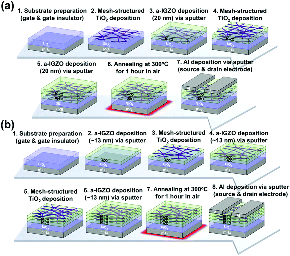
We have developed two types of a-IGZO phototransistors that slightly differ in structures as shown in Fig. 1(a) and (b). Firstly, heavily boron-doped silicon (p+–Si) wafers with a layer of thermally oxidized silicon dioxide (SiO2) about 120 nm were prepared as the substrate where p+–Si and SiO2 are the gate electrode and the gate insulator, respectively. For the first structure [Fig. 1(a)], an m-TiO2 layer was first fabricated on top of the gate insulator. Then, the first layer of the a-IGZO film of about 20 nm was deposited by radiofrequency (RF) magnetron sputtering under 5 mTorr of argon (Ar) plasma without oxygen with a sputtering power of 150 W at room temperature. The IGZO target used in this experiment consisted of indium oxide (In2O3), gallium oxide (Ga2O3), and zinc oxide (ZnO) in a 1![[thin space (1/6-em)]](https://www.rsc.org/images/entities/char_2009.gif) :1:1 ratio. A second layer of m-TiO2 was then fabricated again, and a final a-IGZO film of about 20 nm was deposited as described above. This completes the fabrication of the channel layer of one of the a-IGZO phototransistors. We term this type of phototransistor the highly defective interface (HDI) a-IGZO phototransistor because the first m-TiO2 layer creates a high number of defects at the interface. For the second structure [Fig. 1(b)], all the layers are deposited in the order described, where all the a-IGZO films are around 13 nm: an a-IGZO, m-TiO2, a-IGZO film, m-TiO2, and a-IGZO film. All of the a-IGZO films are deposited as described above. We term this type of phototransistor the oxide-mesh sandwiched (OMS) a-IGZO phototransistor because an oxide-mesh (m-TiO2) is sandwiched between a-IGZO films. After completion of the channel layers for both types, both samples were thermally annealed at 300 °C in air for 1 hour. Finally, aluminium (Al) was deposited as the source and drain electrodes for both types of phototransistors by RF magnetron sputtering. The length and width of the channel were calculated as 150 and 1000 μm, respectively.
:1:1 ratio. A second layer of m-TiO2 was then fabricated again, and a final a-IGZO film of about 20 nm was deposited as described above. This completes the fabrication of the channel layer of one of the a-IGZO phototransistors. We term this type of phototransistor the highly defective interface (HDI) a-IGZO phototransistor because the first m-TiO2 layer creates a high number of defects at the interface. For the second structure [Fig. 1(b)], all the layers are deposited in the order described, where all the a-IGZO films are around 13 nm: an a-IGZO, m-TiO2, a-IGZO film, m-TiO2, and a-IGZO film. All of the a-IGZO films are deposited as described above. We term this type of phototransistor the oxide-mesh sandwiched (OMS) a-IGZO phototransistor because an oxide-mesh (m-TiO2) is sandwiched between a-IGZO films. After completion of the channel layers for both types, both samples were thermally annealed at 300 °C in air for 1 hour. Finally, aluminium (Al) was deposited as the source and drain electrodes for both types of phototransistors by RF magnetron sputtering. The length and width of the channel were calculated as 150 and 1000 μm, respectively.
 |
| | Fig. 1 Fabrication processes of the (a) HDI and (b) OMS a-IGZO phototransistors. | |
Fabrication of mesh-structured TiO2
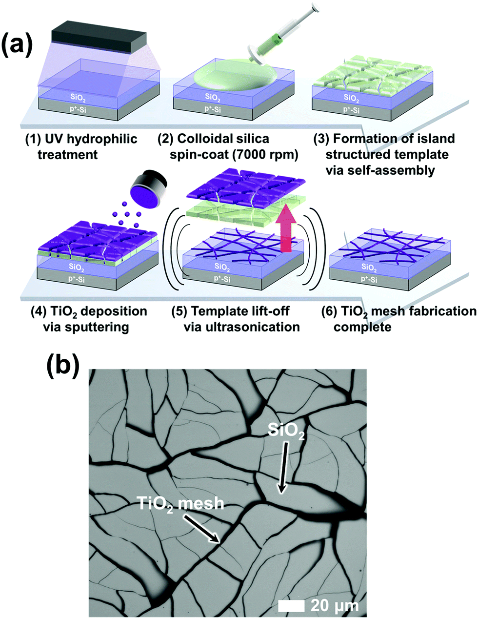
As shown in Fig. 2(a), the samples were exposed to UV light with wavelengths 185 and 254 nm first for 30 minutes to form hydrophilic surfaces on the wafers. Next, colloidal silica was spin-coated onto the wafers, which were dried for about 5 minutes to trigger self-assembly of island formations by self-aggregation of silica nanoparticles. This formed cracked templates on the wafer, where TiO2 of about 8 nm was then deposited by RF magnetron sputtering at 150 W under 5 mTorr of Ar plasma without oxygen. The cracked templates were then lifted-off by ultrasonication in deionized water to form m-TiO2.31Fig. 2(b) shows a scanning electron microscope (SEM) image of m-TiO2 on the wafer.
 |
| | Fig. 2 (a) Fabrication process of the mesh-structured TiO2 on a wafer. (b) SEM image of the mesh-structured TiO2. | |
Measurement and analysis
The electrical properties of all phototransistors were measured using a semiconductor parameter analyser (HP 4156C; Agilent Technologies) in the dark. Also various diode lasers emitting monochromatic light of wavelengths 405, 532, and 635 nm with intensities of 1, 3, 5, and 10 mW mm−2 were employed to measure the photosensing capacity during the electrical property measurements. The endurance of the phototransistor was also measured by applying 0.1 Hz red laser pulse (635 nm) with an intensity of 10 mW mm−2. Also the percentages of metal–oxygen (M–O), oxygen vacancy (Vo), and hydroxide radical (–OH) bonding within the channel layers of all the phototransistors were measured using an X-ray photoelectron spectroscope (XPS; K-Alpha; Thermo Scientific Inc.) to evaluate the formation of Vo where m-TiO2 is inserted. Also the formation of m-TiO2 was observed using an SEM (7610F-Plus; JEOL).
Results and discussion
As mentioned in the introduction, an a-IGZO phototransistor is usually used for UV light detection as an a-IGZO film has a wide band gap of around 3.0 eV. Therefore, we have developed a method for creating subgap states within the band gap of a-IGZO by inserting m-TiO2 inside the channel. This enabled a-IGZO phototransistors to detect visible light because the subgap states absorb energy less than the band gap energy. To obtain an optimal structure, we first fabricated eight different structures as shown in Fig. 3 by changing the locations and number of m-TiO2 layers. Then, we compared the performances of each phototransistor in the dark, under red (635 nm), green (532 nm), and blue (405 nm) lights with an intensity of 10 mW mm−2 with a drain voltage (VD) of 10 V. Among these eight types, two types [Fig. 3(e) and (h)] showed exceptional detection of red light with considerable threshold voltage (Vth) shifts and large differences between ID under light illumination (Iilluminated) and in the dark (Idark) at a gate voltage (VG) of −1 V. They are the HDI and OMS a-IGZO phototransistors that have been described earlier in the Experimental section and are analysed further in this study.
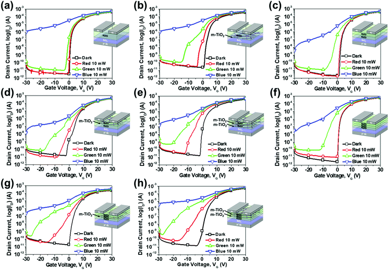 |
| | Fig. 3 Transfer characteristics in the dark and under red (635 nm), green (532 nm), and blue (405 nm) light (intensity 10 mW mm−2) for (a) a-IGZO, (b) a-IGZO/m-TiO2, (c) double a-IGZO, (d) a-IGZO/m-TiO2/a-IGZO, (e) a-IGZO/m-TiO2/a-IGZO/m-TiO2 (HDI), (f) triple a-IGZO, (g) double a-IGZO/m-TiO2/a-IGZO, and (h) a-IGZO/m-TiO2/a-IGZO/m-TiO2/a-IGZO (OMS) phototransistors. | |
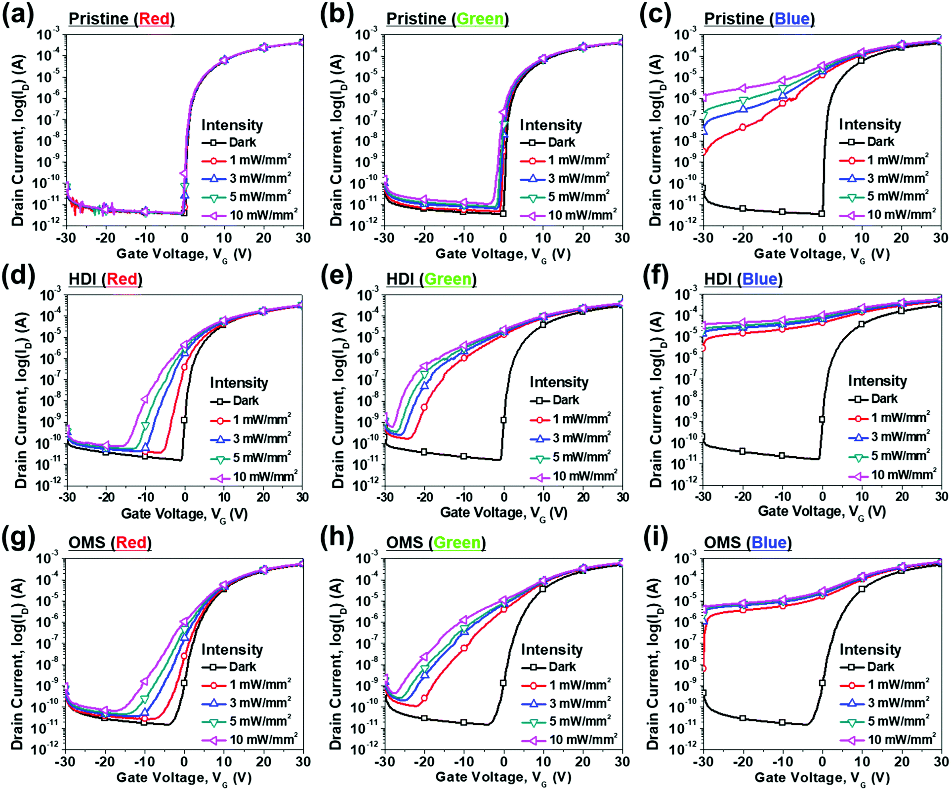
Fig. 4 shows the transfer characteristics of the a-IGZO phototransistors in the dark, under red (635 nm), green (532 nm), and blue (405 nm) light with intensities of 1, 3, 5, and 10 mW mm−2 with a VD of 10 V. Fig. 4 (a)–(c) show the transfer characteristics of the a-IGZO phototransistor without m-TiO2 inserted inside the channel, which we term the pristine a-IGZO phototransistor, under red, green, and blue light, respectively. The pristine phototransistor exhibited high sensitivity to blue light that has enough energy to excite electrons trapped at subgap states that exist deep inside the band gap. However, as the wavelength of the incident light increases, the transfer characteristics show minimal changes because less number of subgap states exists within the band gap where the energy level corresponds to the energy of the incident light. In contrast, the transfer characteristics of both the HDI and OMS a-IGZO phototransistors show considerable changes in Vth and greater differences between Iilluminated and Idark under red, green, and blue light with different intensities [Fig. 4(d)–(i)]. Hence, both types showed improved sensitivity to visible light. Moreover, both types showed improved optoelectronic characteristics compared to the pristine phototransistor, and the HDI was optimal among the three types of phototransistors.
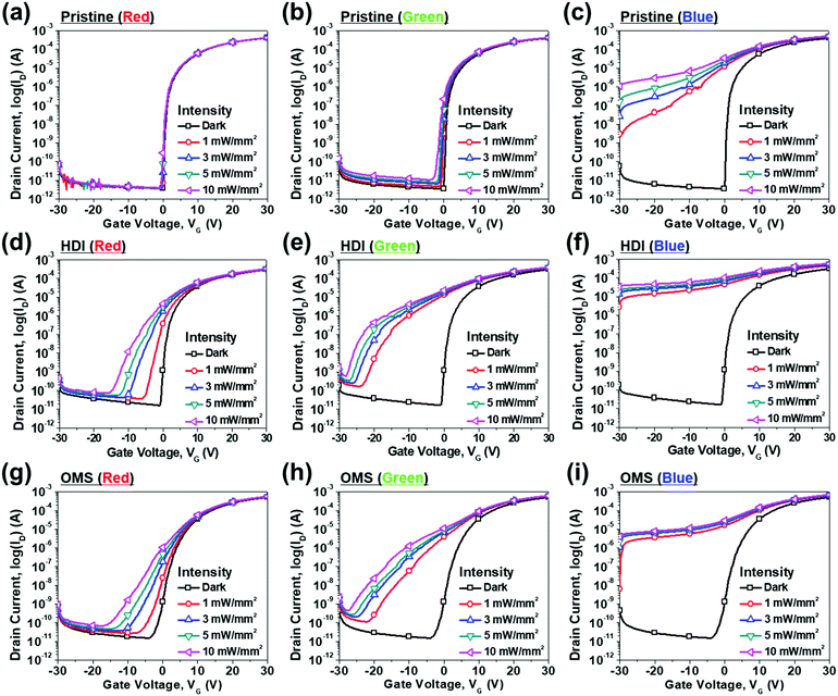 |
| | Fig. 4 Transfer characteristics of the pristine a-IGZO phototransistor under (a) red, (b) green, and (c) blue light with different intensities. Transfer characteristics of the HDI phototransistor under (d) red, (e) green, and (f) blue light with different intensities. Transfer characteristics of the OMS phototransistor under (g) red, (h) green, and (i) blue light with different intensities. | |
There are three parameters that are commonly used to evaluate photosensors: photoresponsivity (PR), photosensitivity (PS), and detectivity (D*). Eqn (1)–(3) define the parameters:
where
Jphoto is the current density during light illumination,
P is the power density of the incident light,
Iphoto =
Iilluminated −
Idark,
q is the absolute value of the charge of an electron (1.6 × 10
−19 C), and
Jdark is the current density in the dark. The electrical properties of all the phototransistors were first measured in the dark. As shown in
Table 1, we have calculated the electrical properties, such as
μFE,
Vth, and subthreshold swing (SS), and optoelectronic properties under red and green lights. For the electrical properties, the extraction methods are explained in the ESI
† (see Fig. S1 for threshold voltage).
32–35
Table 1 Optoelectronic properties of a-IGZO phototransistors
| Sample |
In the dark |
Under red light (635 nm) |
Under green light (532 nm) |
|
μ
FE (cm2 V−1 s−1) |
V
th (V) |
SS (V dec−1) |
N
t (cm−2 eV−1) |
Max. PR (A W−1) |
Max. PS |
Max. D* (Jones) |
Max. PR (A W−1) |
Max. PS |
Max. D* (Jones) |
| Pristine |
9.23 |
1.81 |
0.38 |
9.10 × 10¹¹ |
28.29 |
9.52 × 10 |
2.19 × 10⁷ |
70.38 |
6.07 × 10⁴ |
3.21 × 10⁹ |
| HDI |
6.22 |
1.91 |
0.54 |
1.37 × 10¹² |
178.66 |
1.04 × 10⁵ |
1.25 × 10¹⁰ |
215.77 |
4.38 × 10⁵ |
5.07 × 10¹⁰ |
| OMS |
12.14 |
4.39 |
1.02 |
2.74 × 10¹² |
138.74 |
9.21 × 10³ |
1.44 × 10⁹ |
265.57 |
3.59 × 10⁵ |
4.06 × 10¹⁰ |
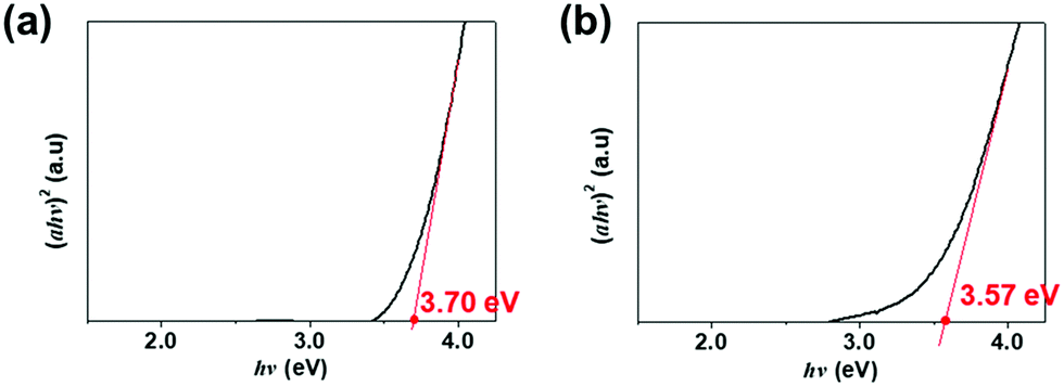
As we can observe, the pristine phototransistor showed the best performance as it lacks defects created by m-TiO2 inside the channel. The HDI showed decreased μFE along with slightly increased Vth and SS. The OMS showed a slightly increased μFE with greatly increased Vth and SS. For the HDI, defects are created directly at the interface of the gate insulator and the channel that serves as the front channel of the TFT where electrons are accumulated and flow during the on-state (VG > Vth). These defects create traps that impede electron flow and decrease μFE. For the OMS, defects are not created directly at the front channel since m-TiO2 is not inserted there, but rather on the top layer. Because of that, m-TiO2 attracts oxygen from the front channel, creating Vo and inducing additional carrier (electron) generation that increases μFE.36,37 On the other hand, the increases in Vth and SS of both the HDI and OMS a-IGZO phototransistors indicate formation of parasitic transistors by m-TiO2. As a well-known semiconductor with a band gap of around 3.2 eV, TiO2 is an n-type semiconductor confirmed by previous studies.24,26–29,38 Since the band gap of m-TiO2 is narrower than the band gap of a-IGZO used in this work which is shown in Fig. 5, current flows through TiO2 before a-IGZO when enough VG is applied to the phototransistors. This also explains the hump observed in the transfer curves as VG required to turn on TiO2 is less than that required to turn on a-IGZO.39,40 Also, greater increases in Vth and SS of the OMS than those of the HDI are explained by the greater number of defects (Nt) inside the channel (2.74 × 1012 cm−2 eV−1 for the OMS, i.e., twice the number of defects of the HDI). The calculation method of Nt is explained in the ESI.†34
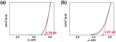 |
| | Fig. 5 Tauc plots of (a) pristine and (b) HDI a-IGZO films. | |
Although defects induced by m-TiO2 insertion caused degradation in transistor performances, they enhanced photosensor performances with the HDI exhibiting the best sensitivity to red light. The PR improved from 28.29 to 178.66 A W−1, the PS from 9.52 × 10 to 1.04 × 10⁵, and the D* from 2.19 × 10⁷ to 1.25 × 10¹⁰ Jones under red light at an intensity of 10 mW mm−2 with a VD of 10 V. Under green light, the PR of the OMS showed higher improvement from 70.38 to 265.57 A W−1 while PR of the HDI improved to 215.77 A W−1. However, the PS and D* were higher for the HDI than the OMS. The PS under green light improved from 6.07 × 10⁴ to 4.38 × 10⁵ and 3.59 × 10⁵ for the HDI and OMS, respectively. D* under green light improved from 3.21 × 10⁹ to 5.07 × 10¹⁰ and 4.06 × 10¹⁰ for the HDI and OMS, respectively. Thus, with the exception of the PR under green light, the HDI a-IGZO phototransistor exhibited the best optoelectronic properties among the three phototransistors.
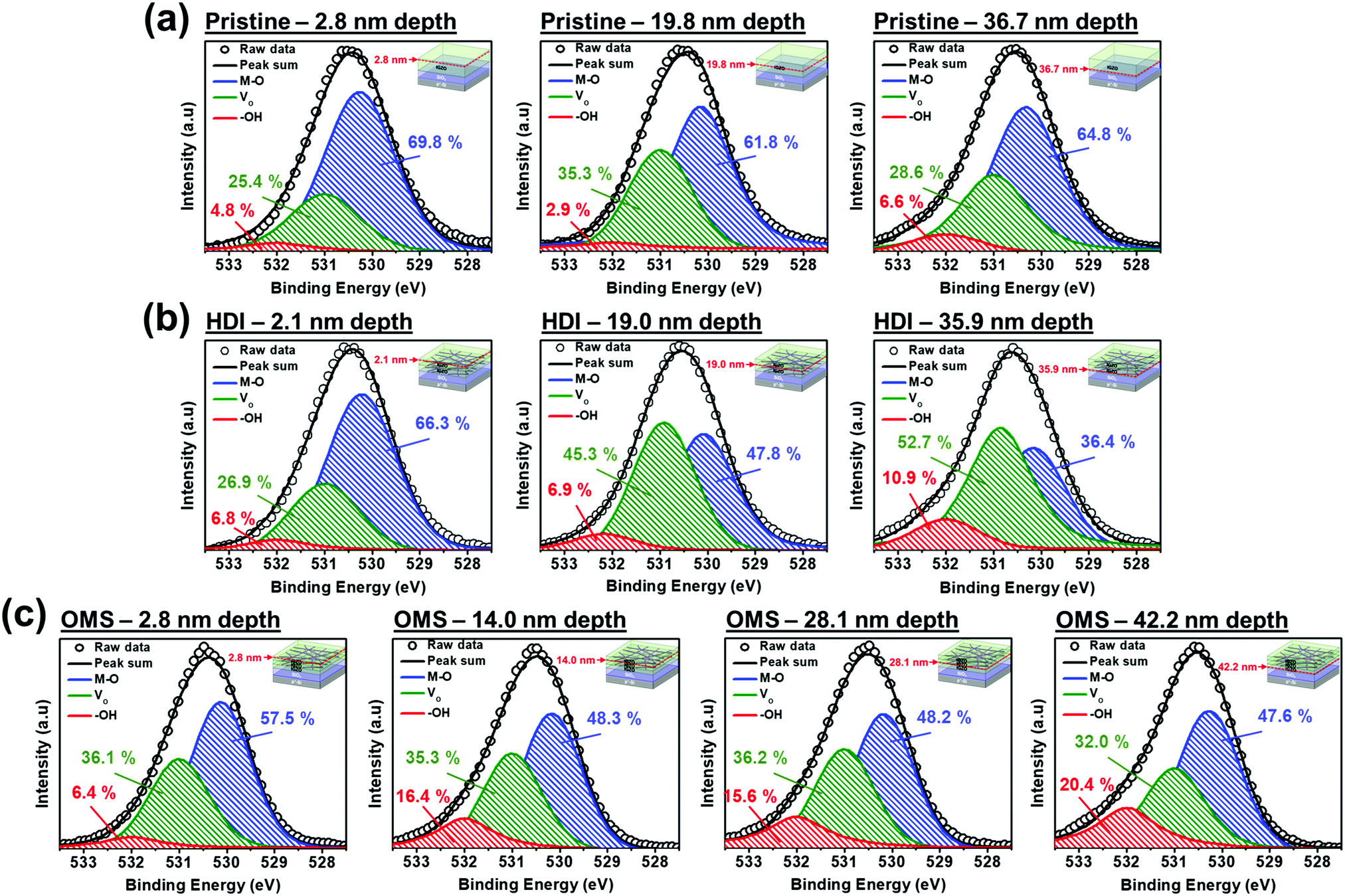
We next investigated why the optoelectronic performance improved by analyzing the XPS depth profiles of the O 1s peaks for all three phototransistors. Fig. 6(a) shows that the channel layer of the pristine a-IGZO phototransistor mostly consisted of M–O bonding and as the depth changes, there are only slight changes in the percentages of M–O bonding, Vo, and –OH bonding. Because the percentage of M–O bonding is dominant among all O 1s peaks, the pristine phototransistor showed the best electrical properties in the dark. Also, the presence of Vo explains its sensitivity to the blue light even though the band gap of the pristine a-IGZO film is around 3.70 eV. Now for both the HDI and OMS a-IGZO phototransistors as shown in Fig. 6(b) and (c), the percentages of M–O bonding decreased significantly from the near-surface (2.1 nm depth for the HDI and 2.8 nm depth for the OMS) to where m-TiO2 was inserted (19.0 and 35.9 nm depths for the HDI and 14.0 and 28.1 nm depths for the OMS). In turn, the percentages of Vo for the HDI increased from the near-surface to the depths mentioned above. For the OMS, Vo stayed almost the same for all the depths but started with higher percentage at the near-surface. For the HDI a-IGZO phototransistor, the increase in the percentage of Vo indicates the formation of subgap states within the band gap of a-IGZO that allow absorption of red light.19 For the OMS a-IGZO phototransistor, the percentage of Vo remained almost the same but started with higher percentage than that of the pristine phototransistor. This is because m-TiO2 in the OMS is inserted nearer to the surface than in the HDI. Also similar to the HDI, this higher percentage of Vo also indicates formation of subgap states. Moreover, the percentages of –OH bonding increased as the depth became deeper. This generation of more –OH bonding is because the defects bonded with hydrogens and generated –OH radicals as both the HDI and OMS a-IGZO phototransistors showed higher percentages than the pristine phototransistor. However, as the percentage of Vo is higher than the percentage of M–O bonding, the HDI a-IGZO phototransistor showed degraded electrical performance in the dark including decreased μFE. As for the OMS, the percentage of M–O bonding was the highest and thus the extra carriers generated by increased amounts of Vo and –OH bonding caused an increase in μFE compared to those of the pristine and the HDI a-IGZO phototransistors.41
 |
| | Fig. 6 De-convoluted O 1s XPS depth profiles at various depths for the channel layers of (a) the pristine, (b) the HDI, and (c) the OMS a-IGZO phototransistors. | |
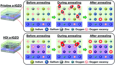
The increased amount of Vo is caused by Ti as it strongly bonds with oxygen (O) than any other element of the a-IGZO film. As a well-known O getter, Ti has a strong Ti–O bond energy of about 7.0 eV whereas In–O, Ga–O, and Zn–O bond energies are 1.7, 2.0, and 1.5 eV, respectively.36,37 Therefore, during thermal annealing of the phototransistors, the O atoms are attracted towards Ti atoms more so than towards In, Ga, or Zn within the a-IGZO film. Thus, more Vos are generated where m-TiO2 is inserted as shown in Fig. 7. From here on, we do not further discuss the OMS a-IGZO phototransistor because the explanation would be redundant with the HDI a-IGZO phototransistor although the number of Vo generated is different.
 |
| | Fig. 7 Comparison of schematic illustrations of the formation of oxygen vacancies at the interface of the a-IGZO and SiO2 layers for the pristine and the HDI a-IGZO phototransistors. | |
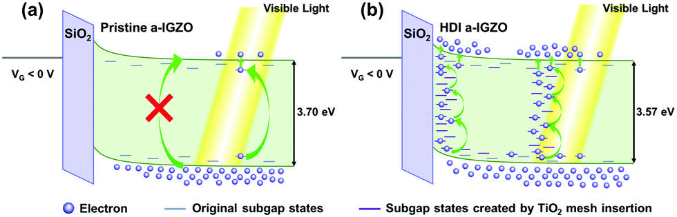
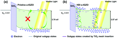
As Vos are formed within the channel of the HDI a-IGZO phototransistor, more subgap states are created within the band gap of a-IGZO as shown in Fig. 8.19,30,36,41 As visible light is illuminated on the phototransistor, the pristine phototransistor cannot absorb it given the large band gap and lack of enough number of subgap states. However, the HDI a-IGZO phototransistor can absorb the light through the abundant number of subgap states which repeatedly trap and excite electrons and contribute them to the photocurrent.
 |
| | Fig. 8 Comparison of operation mechanisms for (a) the pristine and (b) the HDI a-IGZO phototransistors under visible light illumination and VG < 0 V. | |
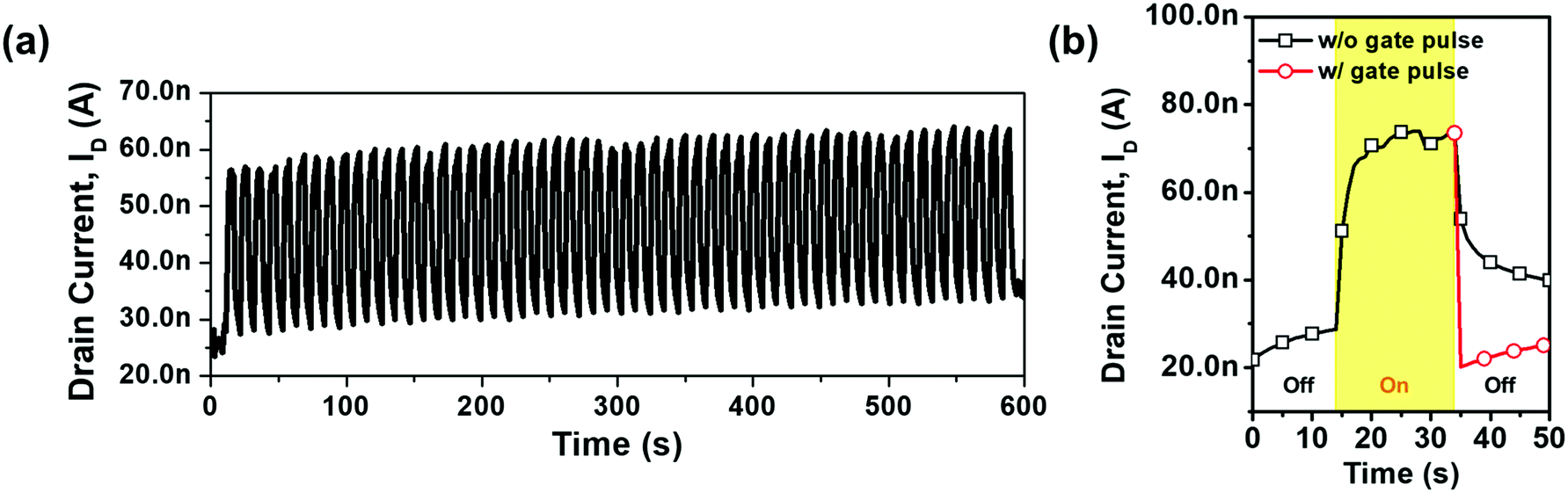
The time-dependent photoresponse characteristic of the HDI a-IGZO phototransistor was investigated by switching the red laser on and off with an intensity of 10 mW mm−2 at a rate of 0.1 Hz. The ID was measured at VG = −1 V and VD = 10 V. As red light is significantly more difficult to detect than any other visible light, measurement under red light is of particular importance compared to any other visible light. However, Fig. 9(a) shows slight increases in both Iilluminated and Idark due to the existence of persistent photocurrent (PPC) originating from the slow recombination due to the traps that exist uniquely in oxide semiconductors.42 As the defects within the HDI a-IGZO phototransistor are deliberately created at the interface of the channel and the gate insulator, electrons become trapped more often, reducing both the response time and recovery time. However, this PPC issue could be resolved by applying a short but highly positive gate pulse bias (+35 V for 5 ms) immediately after the light is turned off [Fig. 9(b)]. This highly positive gate pulse bias induces recombination and detrapping of photoexcited electrons.7,8,15,19,42 After the endurance test, the negative bias stress (NBS) test was also performed to observe the stability of the device under ambient conditions without light at a gate voltage of −1 V, a voltage also used for the endurance tests and for the detection of the light. The NBS tests were performed for the HDI phototransistors as shown in Fig. S2 (ESI†). As the graphs show, there is only a minimal change in the threshold voltage which was about −2.11 V, showing that the ambience has almost no influence under negative bias.43–46 In order to check this, we have also deposited a passivation layer (Y2O3) and tested the stability under NBS. The threshold voltage shift was around −1.48 V, which has reduced but similar enough to show that the ambience has almost no effect on the device under negative bias. On the other hand, for the positive bias stress (PBS) test, the HDI phototransistor showed a significant positive threshold voltage shift of around +8.11 V without passivation. With a passivation layer, the positive threshold voltage shift has reduced to +5.64 V, which indicates that the ambience, mainly oxygen and water molecules,46–49 has a significant effect in addition to the defects that have been made inside the channel layer. However, with a suitable passivation layer, the degradation could be reduced, and thus the device could be used without many problems.19,48–50
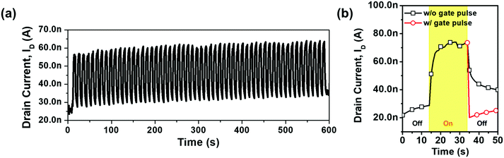 |
| | Fig. 9 (a) Time-dependent photoresponse characteristic of the HDI a-IGZO phototransistor under periodic dark and red light with an intensity of 10 mW mm−2 with a rate of 0.1 Hz for 600 seconds. (b) Comparison of one cycle of photoresponse characteristics with and without a gate pulse bias of +35 V for 5 ms. | |
Conclusions
In conclusion, we developed a-IGZO-based phototransistors that successfully detected wide-wavelength visible light by inserting m-TiO2 inside the channel. We exploited the fact that Ti bonds strongly with O, creating Vo near where TiO2 is formed for the absorption of visible light. Unlike previously developed oxide-based phototransistors, our device does not require a whole extra light absorption layer, but rather we engineered the channel directly. For this reason, the device is highly transparent, consists of simply synthesized materials, and functions relatively well as a transistor. This research has demonstrated that the insertion of an oxide-mesh at the interface of the channel and the gate insulator of an a-IGZO phototransistor increased the number of Vo and thus the number of subgap states absorbing light of lower energy than the actual band gap of the channel material of the device. In future work, we will improve both the photosensor and transistor performance by eliminating transistor degradation that has been shown in this work.
Conflicts of interest
There are no conflicts to declare.
Acknowledgements
This work was supported by the National Research Foundation of Korea (NRF) grant funded by the Korea government (MSIT) (No. 2017R1A2B3008719).
Notes and references
- M. W. Seo, S. W. Choi, S. L. Lee, E. Y. Oh, J. S. Baek and S. J. Kang, Sensors, 2017, 17, 1112 CrossRef PubMed
 .
.
- K. Kasai, Y. Haruyama, T. Yamada, M. Akiba, Y. Tomonari, T. Kaji, T. Terui, F. Peper, S. Tanaka, Y. Katagiri, H. Kikuchi, Y. Okada-Shudo and A. Otomo, Proc. SPIE, 2013, 8817, 88170N CrossRef .
- N. M. Z. Hashim, N. A. Ali, A. Salleh, A. S. Ja’afar and N. A. Z. Abidin, Int. J. Eng. Technol., 2013, 5, 3601 Search PubMed .
- S. Lee, S. Jeon, R. Chaji and A. Nathan, Proc. IEEE, 2015, 103, 644 Search PubMed .
- S. E. Ahn, I. Song, S. Jeon, Y. W. Jeon, Y. Kim, C. Kim, B. Ryu, J. H. Lee, A. Nathan, S. Lee, G. T. Kim and U. I. Chung, Adv. Mater., 2012, 24, 2631 CrossRef CAS PubMed .
- K. Nomura, H. Ohta, A. Takagi, T. Kamiya, M. Hirano and H. Hosono, Nature, 2004, 432, 488 CrossRef CAS PubMed .
- W.-G. Kim, Y. J. Tak and H. J. Kim, J. Inf. Disp., 2018, 19, 39 CrossRef CAS .
- H. Lee, K. S. Chang, Y. J. Tak, T. S. Jung, J. W. Park, W.-G. Kim, J. Chung, C. B. Jeong and H. J. Kim, J. Inf. Disp., 2017, 18, 131 CrossRef CAS .
- Y. Lim, N. Hwang, J. Lee, S. Lee and M. Yi, J. Nanosci. Nanotechnol., 2019, 19, 1470 CrossRef CAS .
- K. M. Kim, W. H. Jeong, D. L. Kim, Y. S. Rim, Y. Choi, M.-K. Ryu, K.-B. Park and H. J. Kim, IEEE Electron Device Lett., 2011, 32, 1242 CAS .
- S. Knobelspies, A. Daus, G. Cantarella, L. Petti, N. Münzenrieder, G. Tröster and G. A. Salvatore, Adv. Electron. Mater., 2016, 2, 1600273 CrossRef .
- Z. Tao, X. Liu, W. Lei and J. Chen, Mater. Lett., 2018, 228, 451 CrossRef CAS .
- H. Zhu, A. Liu, F. Shan, W. Yang, W. Zhang, D. Li and J. Liu, Carbon, 2016, 100, 201 CrossRef CAS .
- H. Lu, X. Zhou, T. Liang, L. Zhang and S. Zhang, IEEE J. Electron Devices Soc., 2017, 5, 504 CAS .
- M. G. Yun, Y. K. Kim, C. H. Ahn, S. W. Cho, W. J. Kang, H. K. Cho and Y. H. Kim, Sci. Rep., 2016, 6, 3199 Search PubMed .
- J. Yang, H. Kwak, Y. Lee, Y. S. Kang, M. H. Cho, J. H. Cho, Y. H. Kim, S. J. Jeong, S. Park, H. J. Lee and H. Kim, ACS Appl. Mater. Interfaces, 2016, 8, 8576 CrossRef CAS PubMed .
- Y. J. Tak, D. J. Kim, W.-G. Kim, J. H. Lee, S. J. Kim, J. H. Kim and H. J. Kim, ACS Appl. Mater. Interfaces, 2018, 10, 12854 CrossRef CAS .
- A. D. Mottram, Y. H. Lin, P. Pattanasattayavong, K. Zhao, A. Amassian and T. D. Anthopoulos, ACS Appl. Mater. Interfaces, 2016, 8, 4894 CrossRef CAS .
- B. H. Kang, W.-G. Kim, J. Chung, J. H. Lee and H. J. Kim, ACS Appl. Mater. Interfaces, 2018, 10, 7223 CrossRef CAS .
- C. H. Ahn., W. J. Kang, Y. K. Kim, M. G. Yun and H. K. Cho, ACS Appl. Mater. Interfaces, 2016, 8, 15518 CrossRef CAS .
- W. D. Sylwestrowicz, J. Electrochem. Soc., 1975, 122, 1504 CrossRef CAS .
- P. A. Crozier, M. R. McCartney and D. J. Smith, Surf. Sci., 1990, 237, 232 CrossRef CAS .
- W. Zhang, J. Mao, W. K. Pang, X. Wang and Z. Guo, Nano Energy, 2018, 49, 549 CrossRef CAS .
- A. M. Selman, Z. Hassan, M. Husham and N. M. Ahmed, Appl. Surf. Sci., 2014, 305, 445 CrossRef CAS .
- Y. Mansourpanah, S. S. Madaeni, A. Rahimpour, A. Farhadian and A. H. Taheri, J. Membr. Sci., 2009, 330, 297 CrossRef CAS .
- A. A. Hendi and F. Yakuphanoglu, J. Alloys Compd., 2016, 665, 418 CrossRef CAS .
- A. M. Selman and Z. Hassan, Sens. Actuators, A, 2015, 221, 15 CrossRef CAS .
- M. Okuya, K. Shiozaki, N. Horikawa, T. Kosugi, G. R. A. Kumora, J. Madarasz, S. Kaneko and G. Pokol, Solid State Ionics, 2004, 172, 527 CrossRef CAS .
- H.-Y. Liu, R.-C. Huang, Y.-Y. Li, C.-S. Lee and W.-C. Hsu, IEEE Electron Device Lett., 2017, 38, 756 CAS .
- J. Yao, N. Xu, S. Deng, J. Chen, J. She, H.-P. D. Shieh, P.-T. Liu and Y.-P. Huang, IEEE Trans. Electron Devices, 2011, 58, 1121 CAS .
- Y.-g. Kim, Y. J. Tak, S. P. Park, H. J. Kim and H. J. Kim, Nanomaterials, 2017, 7, 214 CrossRef .
- A. Ortiz-Conde, F. J. Garcia Sanchez, J. J. Liou, A. Cerdeira, M. Estrada and Y. Yue, Microelectron. Reliab., 2002, 42, 583 CrossRef .
- R. Martins, P. Barquinha, I. Ferreira, L. Pereira, G. Concalves and E. Fortunato, J. Appl. Phys., 2007, 101, 044505 CrossRef .
- G. H. Kim, B. D. Ahn, H. S. Shin, W. H. Jeong, H. J. Kim and H. J. Kim, Appl. Phys. Lett., 2009, 94, 233501 CrossRef .
- J. H. Park, Y.-g. Kim, S. Yoon, S. Hong and H. J. Kim, ACS Appl. Mater. Interfaces, 2014, 6, 21363 CrossRef CAS .
- T. Kamiya, K. Nomura and H. Hosono, Phys. Status Solidi A, 2010, 207, 1698 CrossRef CAS .
- H.-H. Hsu, C.-Y. Chang, C.-H. Cheng, S.-H. Chiou and C.-H. Huang, IEEE Electron Device Lett., 2014, 35, 87 CAS .
- W. S. Shih, S. J. Young, L. W. Ji, W. Water and H. W. Shiu, J. Electrochem. Soc., 2011, 158, 609 CrossRef .
- A. Valletta, P. Gaucci, L. Mariucci, G. Fortunato and F. Templier, J. Appl. Phys., 2008, 104, 124511 CrossRef .
- M. J. Seok, M. Mativenga, D. Geng and J. Jang, IEEE Trans. Electron Devices, 2013, 60, 3787 CAS .
- J. Bang, S. Matsuishi and H. Hosono, Appl. Phys. Lett., 2017, 110, 232105 CrossRef .
- S. Jeon, S. E. Ahn, I. Song, C. J. Kim, U. I. Chung, E. Lee, I. Yoo, A. Nathan, S. Lee, J. Robertson and K. Kim, Nat. Mater., 2012, 11, 301 CrossRef CAS .
- S. Kim, S. Kim, C. Kim, J. Park, I. Song, S. Jeon, S.-E. Ahn, J.-S. Park and J. K. Jeong, Solid-State Electron., 2011, 62, 77 CrossRef CAS .
- J. H. Shin, J.-S. Lee, C.-S. Hwang, S.-H. Ko Park, W.-S. Cheong, M. Ryu, C.-W. Byun, J.-I. Lee and H. Y. Chu, ETRI J., 2009, 31, 62 CrossRef .
- J. Kim, J. Bang, N. Nakamura and H. Hosono, APL Mater., 2019, 7, 022501 CrossRef .
- C.-L. Fan, F.-P. Tseng, B.-J. Li, Y.-Z. Lin, S.-J. Wang, W.-D. Lee and B.-R. Huang, Jpn. J. Appl. Phys., 2016, 55, 02BC17 CrossRef .
- J. K. Jeong, H. W. Yang, J. H. Jeong, Y.-G. Mo and H. D. Kim, Appl. Phys. Lett., 2008, 93, 123508 CrossRef .
- K. Y. Shin, Y. J. Tak, W.-G. Kim, S. Hong and H. J. Kim, ACS Appl. Mater. Interfaces, 2017, 9, 13278 CrossRef CAS .
- S. Hong, S. P. Park, Y.-g. Kim, B. H. Kang, J. W. Na and H. J. Kim, Sci. Rep., 2017, 7, 16265 CrossRef PubMed .
- H. Yoo, Y. J. Tak, W.-G. Kim, Y.-g. Kim and H. J. Kim, J. Mater. Chem. C, 2018, 6, 6187 RSC .
Footnote |
| † Electronic supplementary information (ESI) available. See DOI: 10.1039/c9tc04982g |
|
| This journal is © The Royal Society of Chemistry 2020 |
Click here to see how this site uses Cookies. View our privacy policy here. 
 *
*