
 Open Access Article
 This Open Access Article is licensed under a
 Creative Commons Attribution 3.0 Unported Licence
Image-force effects on energy level alignment at electron transport material/cathode interfaces†
Yongzhen
Chen
 *a,
Xianjie
Liu
a,
Slawomir
Braun
a,
Ying
Wang
b and
Mats
Fahlman
a
*a,
Xianjie
Liu
a,
Slawomir
Braun
a,
Ying
Wang
b and
Mats
Fahlman
a
aLaboratory of Organic Electronics, Department of Science and Technology, Linköping University, 60174 Norrköping, Sweden. E-mail: yongzhen.chen@liu.se
bKey Laboratory of Photochemical Conversion and Optoelectronic Materials, Technical Institute of Physics and Chemistry, Chinese Academy of Sciences, 100190 Beijing, China
First published on 25th November 2019
Abstract
Electron transport materials (ETMs) are widely used as interlayers to lower the cathode electrode work function in organic solar cells and organic light-emitting diodes, for example. The usual interpretation for their operating principle is a chemical interaction between the ETM and the electrode, inducing partial or integer charge transfer or collectively an intrinsic dipole moment caused by preferential molecular orientation. Herein, we systematically explore the commonly used ETM bathophenanthroline (BPhen) deposited on a series of conducting substrates. The energetics at the BPhen interface follows the typical integer charge transfer (ICT) model with an extra displacement of the vacuum level by up to −1.4 eV. The extra displacement is ascribed to the “double dipole step” formed by the positive and negative charged species and their induced image charges when they are close to the surface of substrates. After n-type doping the displacement is further increased to −1.8 eV, yielding a larger work function modification than obtained using typical electrolytes and zwitterions as cathode interlayer.
Introduction
The performance of organic optoelectronic devices is usually limited by the electron injection and transport processes.1 It is hence necessary to reduce the electron injection barrier and/or enhance the transport of electrons. To realize a more effective electron injection, the cathode electrode work function (WF) should match the electron affinity (EA) of the organic semiconductor.2 Aluminum or silver combining with alkali or alkali-earth metals and their salts (such as Ca, Ba, LiF, Cs2CO3, etc.) are commonly used as cathode interlayers in the traditional device structure and show excellent electron-injection properties.3–6 In inverted devices, however, these type of electrodes are rarely used due to issues with optical transparency and device stability. An alternative solution is to use stable metals or metallic oxides modified by polymers or small molecules that can create an interface dipole to lower the work function. Among numerous materials, small molecule electron transport materials (ETMs) are one of the most popular types used. Several ETMs with high electron mobility and appropriate energy levels (often first used in organic light-emitting diodes (OLEDs)) have been developed during the past years, such as bathophenanthroline (BPhen),7,8 bathocuproine (BCP),9–12 1,3,5-tris(2-N-phenylbenzimidazolyl)benzene (TPBi),13 tris-(8-hydroxyquinoline)aluminum (Alq3),14,15 4,6-bis(3,5-di-3-pyridylphenyl)-2-methylpyrimidine (B3PYMPM)16 and 1,3,5-tris(3-pyridyl-3-phenyl)benzene (TmPyPB),17–19etc. N-type doping of these materials are widely used to further improve their performance as cathode interlayers in inverted OLEDs.16,20 Most ETMs can also be applied in organic solar cells (OSCs) as cathode interlayers and present superior performance compared to LiF.21 Interestingly, ETMs can produce interface dipole potential steps even larger than most (non-) conjugated electrolytes and zwitterions that contain ionizable pendant groups and two charged centers and hence feature a sizeable internal charge separation.22–24The mechanism leading to the large interface dipole potential steps is presently a controversial issue. One proposed explanation is the orbital hybridization theory, which states an ETM-metal complex will be generated at the interface when ETMs are deposited onto the surface of metal substrate.25,26 This phenomenon is well known when active metals are evaporated later or together with the ETMs.27–29 Though ultraviolet photoelectron spectroscopy (UPS), gap states between highest occupied molecular orbital (HOMO) and lowest unoccupied molecular orbital (LUMO) are detected and also consistent with the DFT calculation result.28–30 However, this only occurs when the molecules are deposited on clean reactive metal surfaces with low WF, such as BCP on Ag, Al, Ca, Mg. The interface dipoles created by ETMs at the surface of nonreactive metals, e.g., Au, Cu,25 AlOx and organic films,31–34 cannot be explained by this theory, however. Another proposed model is that ETMs with an intrinsic molecular dipole moment can create a dipole potential step through intermolecular order at the interface.35 Researchers also have found that giant surface potentials can exist in amorphous films for some polar organic materials and ascribe the formation mechanism to the spontaneous orientation of molecular dipoles in the bulk.36–39 The latter scenario is not compatible with an observed sharp decrease of WF mainly located in the monolayer interface.
Recently, a detailed investigation has been carried out to explore the formation mechanism of a displacement away from the Schottky–Mott limit of vacuum level alignment. The n-type organic semiconductor fullerene derivatives40 and P(NDI2OD-T2)41 mentioned in the papers all follow the integer charge transfer (ICT) model,42,43i.e., three energy-level alignment regimes where the Fermi level of substrate pinned to positive/negative interface polarons (EICT±) or vacuum level aligned (see Fig. S1a, ESI†). After n-doping or oxygen exposure, they all show an additional downshift in the resulting WF. This downshift is explained by the formation of a so-called “double-dipole step” at the interface. For both n-doping and oxygen exposure, new charged species are formed in the bulk and at the interface. Due to the image force effect, the more mobile (delocalized) charges near the interface will be driven closer to the substrate surface. As a result, the charges and their respective image charges together create the interface “double dipole step” as shown in Fig. S1b (ESI†).44 For the n-doping case, the negative polaron (anion) on the host polymer is more easily delocalized to the surface compared to the large donor molecule (cation); while for the oxygen exposure, the small and highly mobile negatively charged O2 will obtain the more intimate contact to the substrate surface. Both cases produce dipole moments pointing to the organic films and lower the work function efficiently. This interpretation also works on the molecules containing lone electron pairs, e.g., poly(16-fluorene)-alt-2,7-(9,9-dioctylfluorene) (PFN).44,45 The image force effect hence should also be considered for ETMs containing lone electron pairs when contacting with conductive substrates. In this paper, the double dipole step modified ICT model40,41 is used to understand the interface dipole formed by small-molecule ETMs. A planar molecule containing two nitrogen lone pair electrons, BPhen, one of the most widely used ETMs in OLEDs and OSCs, is chosen to reveal the general energy level alignment behavior of such molecules. BPhen shows an intrinsic molecular dipole moment of 4.53 Debye and its chemical structure is depicted Fig. 1. From the photoelectron spectroscopy results, we demonstrate that pristine BPhen interlayers show a 1.4 eV downshift compared to the ideal ICT curve, which we attribute to an interface double dipole step, as the dipole potential step exists only in the first layer of the substrate surface. This step is further amplified by introducing negative charges from a n-type dopant, as previously observed for other systems.46 We evaluate the electron injection efficiency of BPhen and BPhen:Cs2CO3 as cathode interlayers by electron-only and inverted OLED devices, respectively. Their excellent performance agree well with the photoelectron spectroscopy results.
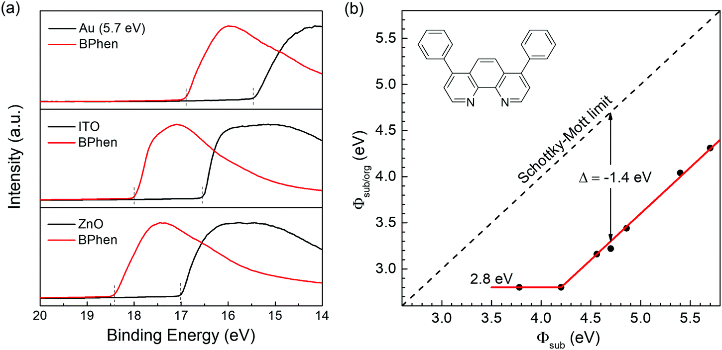 | ||
| Fig. 1 (a) Photoemission cutoff for the secondary electrons of various substrates with and without BPhen. (b) Summary of the Φsub/org changing with Φsub. The fitting line (red) follows well with the ICT model except for a negative displacement (Δ). The inset shows the molecular structure of BPhen. | ||
Experimental details
Materials
BPhen used in this study was purchased from Sigma-Aldrich with purity higher than 99%. C60 was purchased from Luminescence Technology Corp. and purified by gradient sublimation twice before use. ZnO substrate used in UPS measurement was achieved by spin-coating ZnO nanoparticle solution on indium-tin oxide (ITO) coated glass. The various work functions of Au and ITO were achieved by UV–ozone treatment with different time. All other materials were purchased from Luminescence Technology Corp. and used as received.Photoelectron spectroscopy samples and characterization
The thermally-deposited films were fabricated in a vacuum evaporation chamber with pressure below 5 × 10⁻⁷ mbar, and the deposition rate was about 0.04 nm s−1. The spin-coated BPhen films were made from ethanol solution with concentration of 5.0 mg mL−1. UPS was performed in a home-designed spectrometer using monochromatized He I radiation with excitation energy of 21.22 eV. XPS was performed in a Scienta-200 hemispherical analyzer using monochromatized Al Kα radiation of 1486.6 eV energy. All photoelectron spectroscopy measurements were carried out with a base pressure lower than 10−9 mbar.Electron-only and OLED devices
The devices were fabricated on glass substrates precoated with ITO. The substrates were washed with detergent, ultrasonicated in acetone and isopropanol, and followed by UVO treatment. For electron-only device, all organic and electrode layers were prepared in the vacuum evaporation chamber and measured on a Paios platform. For the inverted OLED, the ZnO and Cs2CO3 doped BPhen films were spin-coated in air. And then the substrates were transferred into the evaporation chamber and finished the fabrication of subsequent layers in vacuum. The final structure is: ITO/ZnO/BPhen:Cs2CO3 (20 nm)/BPhen (40 nm)/3,3-di(9H-carbazol-9-yl)biphenyl (mCBP):10 wt% tris(2-phenylpyridine)iridium [Ir(ppy)3] (30 nm)/1,1-bis[(di-4-tolylamino)phenyl]cyclohexane (TAPC) (50 nm)/MoO3 (10 nm)/Al (90 nm), where mCBP is used as the host of phosphorescent emitter Ir(ppy)3, BPhen and TAPC are used as the electron and hole transport layer respectively, and MoO3/Al is used as the anode. The electroluminescence spectra were measured by a Spectra scan PR655 photometer. The current–voltage–brightness characteristics were measured by a computer-controlled Keithley 2400 source meter with a calibrated optical power meter (Newport Co. 1936R) under dark and ambient atmosphere. External quantum efficiencies (EQE, %), current efficiencies (cd A−1) and power efficiencies (lm W−1) were calculated from the electrical and optical properties. For this calculation we assumed Lambertian light distribution.Results and discussion
First, using ultraviolet photoelectron spectroscopy (UPS) we measure the work function of BPhen deposited on a series of substrates. The results are shown in Fig. 1a and Fig. S2 (ESI†). As we can see, there is a large shift of the secondary electron cut-off towards the high binding energy direction after adding 15 nm-thick BPhen for all substrates, which means a decrease of the WF upon BPhen film-formation. In particular, for ITO and ZnO, two widely used transparent electrodes, the WF can be reduced from 4.70 eV and 4.20 eV to 3.22 eV and 2.80 eV, respectively, after adding a thin BPhen film. The resulting WFs are even lower than what is obtained from typical polymeric electrode interlayers (e.g. PEI and PEIE).47 The relationship between the WF of BPhen-on-substrate (Φsub/org) and bare substrate (Φsub) are summarized in Fig. 1b. We obtain a fitting line with two distinct slopes S = 0 and S = 1, which are corresponding to the two regions of Φsub < EICT− and EICT− < Φsub < EICT+ respectively in the ideal ICT curve.43,48,49 When Φsub is smaller than 4.2 eV, the Fermi level is pinned to 2.8 eV. While when Φsub is larger than 4.2 eV, Φsub/org is equal to (Φsub – 1.4) eV. At sufficiently large substrate WF (Φsub > EICT+) the Fermi level should again become pinned, but the WF range of the substrates used did not extend far enough for this to occur. We obtain the same results when measuring films prepared by spin-coating method, as shown in Fig. S3 (ESI†). The same property has been discovered for two other common ETMs:BCP and Alq3 with displacements of −1.6 eV and −0.4 eV, respectively.26,35The thickness dependence of the displacement is studied by UPS, which is shown in Fig. 2a. The measurements are carried out on gold substrates with Φsub in the S = 1 region to eliminate the interference of charge transfer effects. The original gold surfaces are treated by UV-ozone cleaning for 15 min to obtain a high WF of 5.7 eV. After depositing a 0.8 nm-thick BPhen film, the WF decreases to 4.59 eV. Further increasing the thickness to 1.6 nm, the WF additionally is reduced by 0.3 eV, and is fixed at 4.30 eV despite continued film thickness increases. Fig. 2b shows the amplified spectra around the Fermi level, from which we clearly can see the Fermi level of gold for 0.8 nm case, suggesting partial coverage only. For 1.6 nm and the even thicker cases, the Fermi level vanishes completely. This indicates that the WF downshift saturates when the substrate is fully covered with BPhen (monolayer) and does not change with additional layers. In other words, the interface dipole step only occurs in the first layer of the BPhen film, as also observed for thin conjugated polymer films.50 Based on the above results, we then analyze the N 1s core level spectra of BPhen films with different thickness by X-ray photoelectron spectroscopy (XPS). As we can see in Fig. 2c, there is no shifts or new features for the thicknesses of 0.8 and 1.6 nm compared to the 15 nm thickness film. The same phenomenon was observed for oxygen-exposed P(NDI2OD-T2) film.41 This result firmly suggests that no chemical interaction occurs between BPhen and the gold substrate.
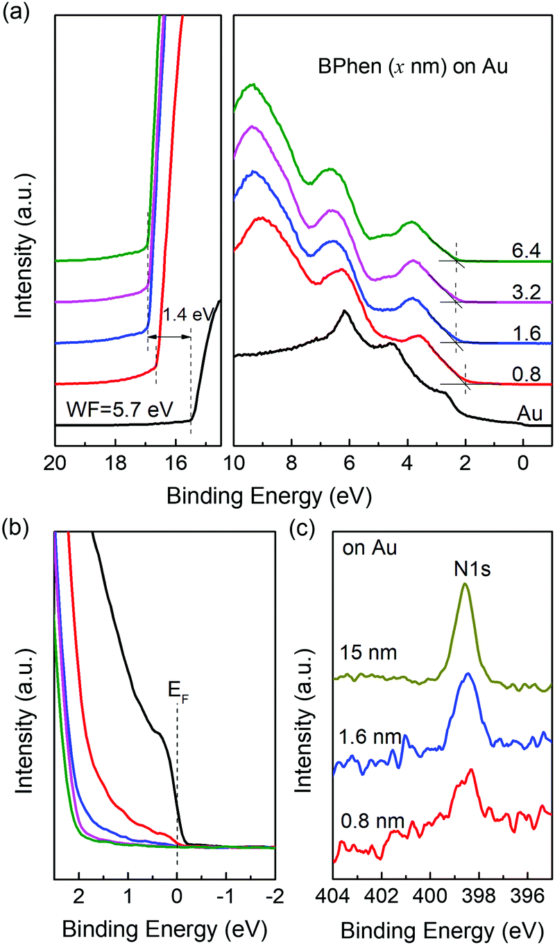 | ||
| Fig. 2 (a) UPS spectra of Au with incrementally deposited BPhen layer. (b) Magnifications of the same spectra near the Fermi level. (c) XPS spectra of BPhen on Au with different thickness. From the spectra we confirmed the large dipole only occurs in the first layer and there is no band bending or chemical interaction near the interface. | ||
The results so far support the interpretation of energy level alignment following the ICT model with the additional formation of a double-dipole step. We then measure the angle-resolved photoemission spectroscopy (ARXPS and ARUPS) to reveal the molecular orientation at the interface. As reported in α-sexithiophene51,52 and pentacene,52,53 the highly ordered films feature different binding energy of valence band and core level as varying the molecular orientation. That means if the interface dipole potential step is caused by the ordered molecule dipoles, the spectra should move as the emission angle changes for thin enough samples with an incomplete top layer. Two samples are studied here, one is not fully covered in the monolayer (<0.8 nm) and another is two- or three-layers thickness (∼2 nm). So that we can clearly see the microstructure of the primary growing stage. As shown in Fig. 3a, by changing the emission angle from 0° to 60°, there is no obvious shift for the valence band, i.e., HOMO peaks overlap very well, in both monolayer and the subsequent layers. The ARXPS results of the thicker film are shown in Fig. 3b and c. For both C 1s and N 1s spectra, their performances are consistent with the UPS results that show no shift by varying the emission angles. The same results are also observed in the monolayer, as shown in Fig. S4 (ESI†). All the results demonstrate that no regular molecular orientation, or at least no preferential standing orientation exists at the interface. Note that the electrostatic potential changes little with varying emission angles for lying molecules with π-electron clouds extending out of the molecular plane, which is quite different from the standing case,50 making it difficult to differentiate between randomly ordered or preferentially lying films using ARUPS. Nevertheless, as a standing orientation is excluded by the combined ARXPS/ARUPS data, the interface dipole is not produced by the ordered molecular dipoles. In addition, we prepare another sample with thickness of about 8 nm, so that the deepest detection molecules are located in the first few layers near the substrate when changing the emission angles. If these molecules are arranged along the direction perpendicular to the substrate, the atomic ratios of C![[thin space (1/6-em)]](https://www.rsc.org/images/entities/char_2009.gif) :N should show a regular change with the variation of emission angles. By integrating the peak areas of C 1s and N 1s, however, we don’t observe any change of the atomic ratios at different emission angles. We only show the results measured at 0° and 60° in Fig. S5 (ESI†). This result further confirms that the BPhen molecules are randomly arranged in the vertical direction.
:N should show a regular change with the variation of emission angles. By integrating the peak areas of C 1s and N 1s, however, we don’t observe any change of the atomic ratios at different emission angles. We only show the results measured at 0° and 60° in Fig. S5 (ESI†). This result further confirms that the BPhen molecules are randomly arranged in the vertical direction.
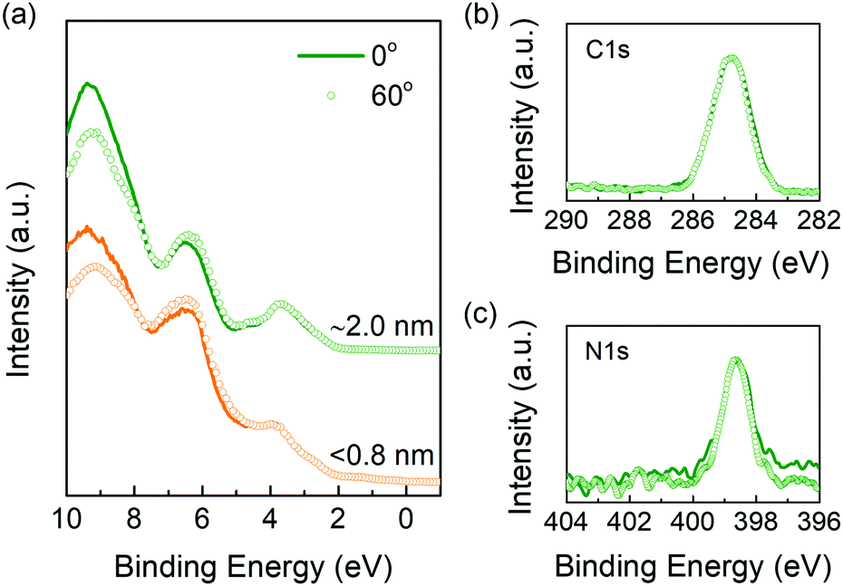 | ||
| Fig. 3 (a) Comparison of ARUPS spectra for samples with less than 0.8 nm- and 2.0 nm-thick films at emission angles of 0° and 60°. ARXPS spectra of C 1s (b) and N 1s (c) for the 2.0 nm-thick sample at emission angles of 0° and 60°. | ||
To better understand the formation of the “double dipole step” in amorphous film, a schematic illustration is given in Fig. 4. Two nitrogen atoms in BPhen molecule feature free electron lone pairs in sp2 orbitals that overlap little with the aromatic π-system. The lone pairs together with two nitrogen nuclei compose the negative and positive species. When molecules are deposited onto the substrate, the two species will be toward, parallel or away from the surface, as shown in Fig. 4a. Due to the image force effect depends highly on the distance from the charge to the metal surface, i.e., the magnitude of the force is inversely proportional to this distance, it can be negligible when nitrogen atoms are away from the substrate compared to the case that they are close to the substrate. Accordingly, only BPhen molecules with their nitrogen atoms close to the surface of the substrate (e.g. the leftmost three in Fig. 4a) are effective to create the “double dipole step”. As the positive and negative charge centers rotating from vertical to parallel to the substrate surface, the dipole moment in the vertical direction will decrease continuously. When the BPhen molecules are face-down parallel to the substrate, the wave functions of the lone pair electrons extend out and down further than the (proton) wave functions of the nitrogen nuclei (driven by the image force), so that a weak dipole step still can be created in this case. The lone electron pairs and nuclei will induce positive and negative charges in the substrate side, respectively, and their arrangement is shown in Fig. 4b. The double dipole moments point from substrate to BPhen film, inducing a downshift of vacuum level at the interface. The formation mechanism is similar to PFN, which features lone pair electrons in sp3 orbitals of tertiary amines.45
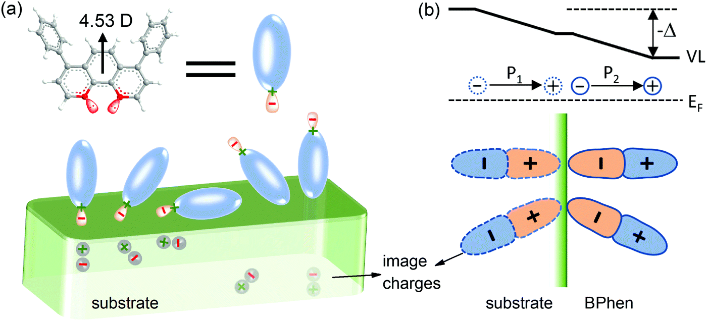 | ||
| Fig. 4 Schematic illustration of the formation mechanism for the interface dipole. The dipole moment marked in (a) is obtained by density functional theory (DFT) calculations with a basis set of B3LYP/6-31G**. Only molecules with lone pairs close to the substrate surface (left three cases) can create a “double dipole step”. The arrangement of charges at the interface is shown in (b). The dipoles point from substrate to the BPhen film both for the charged species (BPhen side) and their image charges (substrate side), inducing a large downshift of the vacuum level. | ||
To investigate the electron-injection capability of BPhen modified cathodes in OSCs, we fabricate electron-only devices using BPhen-coated ITO as bottom electrode. The device structure is ITO/BPhen (x nm)/C60 (100 nm)/LiF (1.2 nm)/Al. A comparison of current density–voltage (J–V) characteristics for devices with different thickness of BPhen is shown in Fig. 5a. As expected, the device without BPhen shows a low current density when injecting from ITO side due to the high electron-injection barrier from Fermi level of ITO (Φ = 4.7 eV) to the LUMO of C60 (3.96 eV).54 After adding a thin BPhen layer, the electron injection from ITO is improved considerably, and the current density is comparable to the LiF/Al side. Due to the improved conductivity compared to the typical polymeric cathode interlayers (e.g. PEI, PEIE), BPhen as an interlayer to improve the electron-injection efficiency is relatively independent of thickness. Hence, a device with a 10 nm-thick BPhen interlayer performs similarly to 5 nm BPhen devices. The decrease of the injection barrier is well observed in the UPS (Fig. 5b), which shows a lower WF after inserting the BPhen layer to facilitate electron injection. This result implies that BPhen modified ITO can be applied as cathode in inverted small-molecule OSCs.
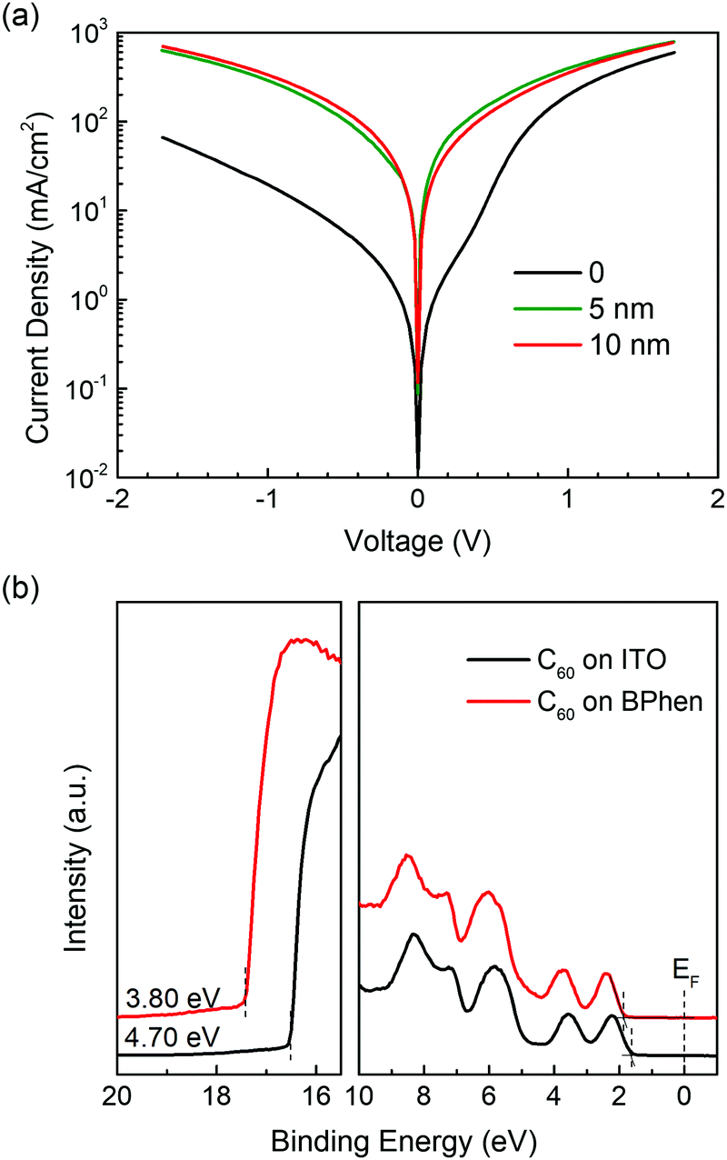 | ||
| Fig. 5 (a) Current density–voltage characteristics of ITO/BPhen/C60/LiF/Al electron-only device with varying BPhen thickness. Negative bias corresponds to electron injecting from ITO side. (b) Comparison of UPS spectra for C60 on ITO and ITO/BPhen. | ||
Finally, we study the n-doping effect on the interface dipole because the dopant can provide additional electrons to BPhen and further enlarge the interface dipole, in accordance with the previous studies of n-doped organic semiconductors.40 Here, we choose an alkali metal salt Cs2CO3 as the dopant and the concentration is 10 wt%. The BPhen:Cs2CO3 mixed films are prepared on different substrates by spin-coating method and characterized by UPS. The spectra for samples with and without BPhen are shown in Fig. S6 (ESI†) and summarized in Fig. 6a. N-doped BPhen also follows the general ICT model behavior with a negative displacement. The difference is that the displacement is increased to −1.8 eV, which means a larger interface dipole, as expected from the model.46 What's more exciting is that the Fermi level is pinned closely to the bulk EA of BPhen when using ZnO and aluminum as electrodes. It means that it is low enough to inject electrons to most ETMs or host materials in OLEDs. To verify this point, we designed an inverted OLED using the structure: ITO/ZnO (20 nm)/BPhen:10 wt% Cs2CO3 (20 nm)/BPhen (40 nm)/mCBP:Ir(ppy)3 (30 nm)/TAPC (50 nm)/MoO3 (10 nm)/Al (90 nm). The electroluminescence characteristics are shown in Fig. 6b and Fig. S7 (ESI†) and summarized in Table S1 (ESI†). The maximum external quantum efficiency (EQE) and current efficiency of the device reach to 20.8% and 72.5 cd A−1, respectively, and can maintain high values of 11.8% and 41.2 cd A−1 even at an ultrahigh luminance of 10000 cd m−2. The low efficiency roll-off is ascribed to the improved electron injection and the thicker emitting layer as the recombination region of electrons and holes will move to the hole transport layer/emitting layer interface at a higher voltage if a barrier for electron injection exist causing exciton–exciton annihilation at a high brightness.
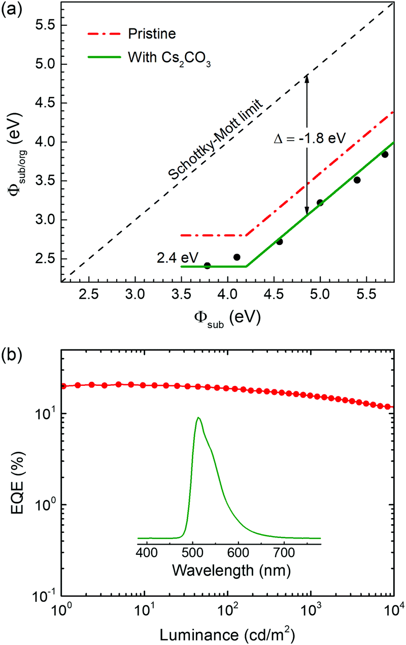 | ||
| Fig. 6 (a) Summary of the Φsub/org changing with Φsub for Cs2CO3 doped BPhen. (b) External quantum efficiency versus luminance of the Ir(ppy)3-based inverted OLED. The inset is the electroluminescence spectrum at 1000 cd m−2. | ||
Conclusions
In summary, we analyzed the interface dipole of a typical electron transport material BPhen and proposed a new insight into its formation mechanism. The ICT model and a “double dipole step” induced by image force effect can explain the observed behavior. In detail, the interface dipole is composed of two parts: (i) a dipole caused by the integer charge transfer to get Fermi level alignment, only existing when Φsub < EICT− or Φsub > EICT+; (ii) an additional dipole step created by the nitrogen lone pair electrons and nuclei and their induced image charges when they are located close to the substrate surface. We find that the dipole will increase from −1.4 eV to −1.8 eV when doped by Cs2CO3, as expected from the model as we introduce additional charged species in the interface layer. As a test of our UPS results and model, we fabricate devices using BPhen-modified ITO and BPhen:Cs2CO3-modified ZnO as cathodes. Both types of devices show excellent electron injection characteristics as predicted by the model and UPS results. We expect our study to provide some help in better understanding the energetics at ETMs/cathode interfaces and help design of ETM materials and devices.Conflicts of interest
There are no conflicts to declare.Acknowledgements
This work was financed by the Knut and Alice Wallenberg Foundation project “Tail of the Sun”, the Swedish Research Council (project grant no. 2016-05498), the Swedish Foundation for Strategic Research SE13-0060, the Ministry of Science and Technology (no. 2016YFA0200700), the NSFC (21504066 and 21534003), the Swedish Energy Agency (grant. no. 45411-1) and the Swedish Government Strategic Research Area in Materials Science on Functional Materials at Linköping University (Faculty Grant SFO Mat LiU no. 2009 00971).Notes and references
- A. P. Kulkarni, C. J. Tonzola, A. Babel and S. A. Jenekhe, Chem. Mater., 2004, 16, 4556–4573 CrossRef CAS.
- A. Atxabal, S. Braun, T. Arnold, X. Sun, S. Parui, X. Liu, C. Gozalvez, R. Llopis, A. Mateo-Alonso, F. Casanova, F. Ortmann, M. Fahlman and L. E. Hueso, Adv. Mater., 2017, 29, 1606901 CrossRef.
- S. K. M. Jönsson, E. Carlegrim, F. Zhang, W. R. Salaneck and M. Fahlman, Jpn. J. Appl. Phys., 2005, 44, 3695–3701 CrossRef.
- C.-I. Wu, C.-T. Lin, Y.-H. Chen, M.-H. Chen, Y.-J. Lu and C.-C. Wu, Appl. Phys. Lett., 2006, 88, 152104 CrossRef.
- V. Gupta, A. K. Kyaw, D. H. Wang, S. Chand, G. C. Bazan and A. J. Heeger, Sci. Rep., 2013, 3, 1965 CrossRef.
- H. Ju, K. M. Knesting, W. Zhang, X. Pan, C. H. Wang, Y. W. Yang, D. S. Ginger and J. Zhu, ACS Appl. Mater. Interfaces, 2016, 8, 2125–2131 CrossRef CAS.
- Y.-Q. Li, Q.-K. Wang, Q.-D. Ou and J.-X. Tang, Sci. China: Chem., 2016, 59, 422–435 CrossRef CAS.
- E. Collado-Fregoso, S. N. Pugliese, M. Wojcik, J. Benduhn, E. Bar-Or, L. Perdigon Toro, U. Hormann, D. Spoltore, K. Vandewal, J. M. Hodgkiss and D. Neher, J. Am. Chem. Soc., 2019, 141, 2329–2341 CrossRef CAS.
- H. Gommans, B. Verreet, B. P. Rand, R. Muller, J. Poortmans, P. Heremans and J. Genoe, Adv. Funct. Mater., 2008, 18, 3686–3691 CrossRef CAS.
- A. Martínez-Otero, X. Elias, R. Betancur and J. Martorell, Adv. Opt. Mater., 2013, 1, 37–42 CrossRef.
- X. Hao, S. Wang, T. Sakurai and K. Akimoto, Jpn. J. Appl. Phys., 2015, 54, 04dk06 CrossRef.
- S. Engmann, A. J. Barito, E. G. Bittle, N. C. Giebink, L. J. Richter and D. J. Gundlach, Nat. Commun., 2019, 10, 227 CrossRef.
- Z. Gao, C. S. Lee, I. Bello, S. T. Lee, R.-M. Chen, T.-Y. Luh, J. Shi and C. W. Tang, Appl. Phys. Lett., 1999, 74, 865–867 CrossRef CAS.
- P. Vivo, J. Jukola, M. Ojala, V. Chukharev and H. Lemmetyinen, Sol. Energy Mater. Sol. Cells, 2008, 92, 1416–1420 CrossRef CAS.
- V. M. Manninen, W. A. E. Omar, J. P. Heiskanen, H. J. Lemmetyinen and O. E. O. Hormi, J. Mater. Chem., 2012, 22, 22971 RSC.
- J.-H. Lee, P.-S. Wang, H.-D. Park, C.-I. Wu and J.-J. Kim, Org. Electron., 2011, 12, 1763–1767 CrossRef CAS.
- H.-W. Lin, C.-W. Lu, L.-Y. Lin, Y.-H. Chen, W.-C. Lin, K.-T. Wong and F. Lin, J. Mater. Chem. A, 2013, 1, 1770–1777 RSC.
- X. Che, Y. Li, Y. Qu and S. R. Forrest, Nat. Energy, 2018, 3, 422–427 CrossRef CAS.
- Y. Li, J. D. Lin, X. Liu, Y. Qu, F. P. Wu, F. Liu, Z. Q. Jiang and S. R. Forrest, Adv. Mater., 2018, 30, 1804416 CrossRef.
- Y. Chen, X. Wei, Z. Li, Y. Liu, J. Liu, R. Wang, P. Wang, Y. Yamada-Takamura and Y. Wang, J. Mater. Chem. C, 2017, 5, 8400–8407 RSC.
- N. Wang, J. Yu, Y. Zang, J. Huang and Y. Jiang, Sol. Energy Mater. Sol. Cells, 2010, 94, 263–266 CrossRef CAS.
- J. Tao, N. Ali, K. Chen, Z. Huai, Y. Sun, G. Fu, W. Kong and S. Yang, J. Mater. Chem. A, 2019, 7, 1349–1355 RSC.
- H. X. Wei, F. S. Zu, Y. Q. Li, W. C. Chen, Y. Yuan, J. X. Tang, M. K. Fung, C. S. Lee and Y. Y. Noh, Phys. Chem. Chem. Phys., 2016, 18, 4045–4050 RSC.
- G. W. Kim, Y. H. Son, H. I. Yang, J. H. Park, I. J. Ko, R. Lampande, J. Sakong, M.-J. Maeng, J.-A. Hong, J. Y. Lee, Y. Park and J. H. Kwon, Chem. Mater., 2017, 29, 8299–8312 CrossRef CAS.
- S. Toyoshima, K. Kuwabara, T. Sakurai, T. Taima, K. Saito, H. Kato and K. Akimoto, Jpn. J. Appl. Phys., 2007, 46, 2692–2695 CrossRef CAS.
- T. Sakurai, S. Toyoshima, H. Kitazume, S. Masuda, H. Kato and K. Akimoto, J. Appl. Phys., 2010, 107, 043707 CrossRef.
- Z. Bin, G. Dong, P. Wei, Z. Liu, D. Zhang, R. Su, Y. Qiu and L. Duan, Nat. Commun., 2019, 10, 866 CrossRef.
- H. Yoshida, J. Phys. Chem. C, 2015, 119, 24459–24464 CrossRef CAS.
- J. Lee, S. Park, Y. Lee, H. Kim, D. Shin, J. Jeong, K. Jeong, S. W. Cho, H. Lee and Y. Yi, Phys. Chem. Chem. Phys., 2016, 18, 5444–5452 RSC.
- M. D. Bhatt, S. Suzuki, T. Sakurai and K. Akimoto, Appl. Surf. Sci., 2010, 256, 2661–2667 CrossRef CAS.
- S. O. Jeon, J.-H. Kim, J. W. Kim, Y. Park and J. Y. Lee, J. Phys. Chem. C, 2011, 115, 18789–18794 CrossRef CAS.
- Y. Nakayama, T. L. Nguyen, Y. Ozawa, S. I. Machida, T. Sato, H. Tokairin, Y. Noguchi and H. Ishii, Adv. Energy Mater., 2014, 4, 1301354 CrossRef.
- J.-P. Yang, Y. Xiao, Y.-H. Deng, S. Duhm, N. Ueno, S.-T. Lee, Y.-Q. Li and J.-X. Tang, Adv. Funct. Mater., 2012, 22, 600–608 CrossRef CAS.
- Z. Huai, L. Wang, Y. Sun, R. Fan, S. Huang, X. Zhao, X. Li, G. Fu and S. Yang, ACS Appl. Mater. Interfaces, 2018, 10, 5682–5692 CrossRef CAS PubMed.
- L. Lindell, D. Çakır, G. Brocks, M. Fahlman and S. Braun, Appl. Phys. Lett., 2013, 102, 223301 CrossRef.
- H. Ishii, N. Hayashi, E. Ito, Y. Washizu, K. Sugi, Y. Kimura, M. Niwano, Y. Ouchi and K. Seki, Phys. Status Solidi A, 2004, 201, 1075–1094 CrossRef CAS.
- E. Ito, Y. Washizu, N. Hayashi, H. Ishii, N. Matsuie, K. Tsuboi, Y. Ouchi, Y. Harima, K. Yamashita and K. Seki, J. Appl. Phys., 2002, 92, 7306–7310 CrossRef CAS.
- Y. Tanaka, Y. Noguchi, K. Oda, Y. Nakayama, J.-I. Takahashi, H. Tokairin and H. Ishii, J. Appl. Phys., 2014, 116, 114503 CrossRef.
- Y. Noguchi, W. Brütting and H. Ishii, Jpn. J. Appl. Phys., 2019, 58, Sf0801 CrossRef CAS.
- Q. Bao, X. Liu, S. Braun, Y. Li, J. Tang, C. Duan and M. Fahlman, ACS Appl. Mater. Interfaces, 2017, 9, 35476–35482 CrossRef CAS.
- Q. Bao, X. Liu, S. Braun, J. Yang, Y. Li, J. Tang, C. Duan and M. Fahlman, ACS Appl. Mater. Interfaces, 2018, 10, 6491–6497 CrossRef CAS.
- M. Fahlman, A. Crispin, X. Crispin, S. K. Henze, M. P. de Jong, W. Osikowicz, C. Tengstedt and W. R. Salaneck, J. Phys.: Condens. Matter, 2007, 19, 183202 CrossRef CAS.
- S. Braun, W. R. Salaneck and M. Fahlman, Adv. Mater., 2009, 21, 1450–1472 CrossRef CAS.
- S. van Reenen, S. Kouijzer, R. A. J. Janssen, M. M. Wienk and M. Kemerink, Adv. Mater. Interfaces, 2014, 1, 1400189 CrossRef.
- Q. Bao, X. Liu, E. Wang, J. Fang, F. Gao, S. Braun and M. Fahlman, Adv. Mater. Interfaces, 2015, 2, 1500204 CrossRef.
- Q. Bao, X. Liu, S. Braun, F. Gao and M. Fahlman, Adv. Mater. Interfaces, 2015, 2, 1400403 CrossRef.
- Y. Zhou, C. Fuentes-Hernandez, J. Shim, J. Meyer, A. J. Giordano, H. Li, P. Winget, T. Papadopoulos, H. Cheun, J. Kim, M. Fenoll, A. Dindar, W. Haske, E. Najafabadi, T. M. Khan, H. Sojoudi, S. Barlow, S. Graham, J.-L. Brédas, S. R. Marder, A. Kahn and B. Kippelen, Science, 2012, 336, 327–332 CrossRef CAS.
- Q. Bao, S. Braun, C. Wang, X. Liu and M. Fahlman, Adv. Mater. Interfaces, 2018, 6, 1800897 CrossRef.
- M. Fahlman, S. Fabiano, V. Gueskine, D. Simon, M. Berggren and X. Crispin, Nat. Rev. Mater., 2019, 4, 627–650 CrossRef CAS.
- Q. Bao, S. Fabiano, M. Andersson, S. Braun, Z. Sun, X. Crispin, M. Berggren, X. Liu and M. Fahlman, Adv. Funct. Mater., 2016, 26, 1077–1084 CrossRef CAS.
- S. Duhm, G. Heimel, I. Salzmann, H. Glowatzki, R. L. Johnson, A. Vollmer, J. P. Rabe and N. Koch, Nat. Mater., 2008, 7, 326–332 CrossRef CAS.
- G. Heimel, I. Salzmann, S. Duhm and N. Koch, Chem. Mater., 2011, 23, 359–377 CrossRef CAS.
- K. Yamada, S. Yanagisawa, T. Koganezawa, K. Mase, N. Sato and H. Yoshida, Phys. Rev. B, 2018, 97, 245206 CrossRef CAS.
- Z.-L. Guan, J. B. Kim, H. Wang, C. Jaye, D. A. Fischer, Y.-L. Loo and A. Kahn, Org. Electron., 2010, 11, 1779–1785 CrossRef CAS.
Footnote |
| † Electronic supplementary information (ESI) available: A brief introduction of the ICT model and “double dipole step” model; UPS spectra of spin-coated BPhen and Cs2CO3 doped BPhen on a series of substrates; ARXPS spectra for the samples with less than 0.8 nm and 8 nm films; inverted OLED structure and current density–voltage–luminance curves; summary of the OLED performance (PDF). See DOI: 10.1039/c9tc05128g |
| This journal is © The Royal Society of Chemistry 2020 |