
Sequential molecular doping of non-fullerene organic solar cells without hole transport layers†
Dongyang
Zhang
a,
Jianqiu
Wang
ab,
Xuning
Zhang
a,
Jiyu
Zhou
a,
Saud-Uz
Zafar
 b,
Huiqiong
Zhou
b and
Yuan
Zhang
*a
b,
Huiqiong
Zhou
b and
Yuan
Zhang
*a
aSchool of Chemistry, Beijing Advanced Innovation Center for Biomedical Engineering Beihang University, No. 37 Xueyuan Road, Beijing 100191, P. R. China. E-mail: yuanzhang@buaa.edu.cn
bKey Laboratory of Nanosystem and Hierachical Fabrication, CAS Center for Excellence in Nanoscience, National Center for Nanoscience and Technology, Beijing 100190, P. R. China
First published on 11th November 2019
Abstract
While molecular doping has shown the capability to modulate the optoelectrical properties in conjugated polymers or small molecules, some of the widely used dopants (e.g. F4-TCNQ) tend to lead to rapid aggregation in doped host films, forming clusters or large particles which unfavorably impair the morphology and device performance in organic solar cells (OSCs). Here, we report a more gentle doping approach i.e. sequential molecular doping that enables the semiconductive properties of photoactive layers to be modified with negligible damage to the bulk film morphology. Based on a model system of PBDB-T:ITIC bulk heterojunctions, the power conversion efficiency (PCE) of sequentially doped devices with a MoOx hole transporting layer (HTL) is increased to 10.66% (compared to the PCE = 10.01% of the MoOx-containing control device). By controlling the penetration of the dopants, F6-TCNNQ doped devices without MoOx HTLs can produce a PCE of ∼10%, which is comparable to that of the reference cell. The applied sequential doping is mainly found to affect the number of background carriers and the charge transport balance in the doped OSCs, with which carrier extraction is promoted with reduced charge recombination. The results obtained in this work provide a simple methodology for realizing high-efficiency non-fullerene OSCs without using thermally evaporated HTLs.
Introduction
Organic solar cells (OSCs) with a bulk heterojunction (BHJ) structure have attracted considerable attention,1–6 due to the merits of light-weight, flexibility, and optical transparency and potential for low-cost device fabrication. The development of new materials, especially non-fullerene electron acceptors, has led to OSCs that exhibit power conversion efficiencies (PCEs) of more than 16%.7,8 In addition to material designs, adopting ternary BHJs, interface modification or device structure engineering have enabled one to obtain further improved device performance.9–11 Moreover for these strategies, molecular doping has shown the capability to modify the carrier transport and interfacial properties or even the film morphology in organic semiconductors,12–14 which in terms of the special area where dopants are introduced is categorized into bulk or interfacial doping.13,15Among the existing charge transfer p-dopants, F4-TCNQ (2,3,5,6-tetrafluoro-7,7,8,8-tetracyanoquinodimethane) exhibits satisfactory material stability and strong electron-withdrawing ability with a deep-lying lowest unoccupied molecular orbital (LUMO), thus being widely used in organic light-emitting diodes (OLEDs) or field-effect transistors (FETs).16–18 Referring to OSCs, bulk doping with F4-TCNQ has been applied to a few specific BHJ systems with positive effects;12,13 a general worry is that changes in the film morphology in the F4-TCNQ doped blend films may cause the PCE to decrease.19 Moreover, the presence of F4-TCNQ dopants in the polymer solution can decrease the solubility of host compounds, triggering film formation difficulties.20 It was found that mixed polymer and dopant solutions tend to lead to rapid aggregation, forming clusters or large particles even at low concentrations.21–23 These phenomena further impose challenges for applying F4-TCNQ based bulk doping for OSCs while maintaining the desired morphology.24 To prevent aggregation induced by the dopants, a hot-film casting method needs to be applied.25 However, the heating process may reduce the doping efficiency of F4-TCNQ.26
To generate targeted electrical modification, a sequential molecular doping method was confirmed to be an alternate for doping an organic semiconductor. In the P3HT:F4-TCNQ system, researchers found that sequential doping produces significantly more uniform films on the nanoscale compared to bulk doping methods. Interestingly, sequentially doped films show 3–15 times higher electrical conductivities (σ) than bulk doping conductivities at the same dopant levels.19 Based on phosphomolybdic acids (PMAs) as a dopant, Kolesov et al. proposed a sequential doping method, by which the electrical properties and photooxidation stability of fullerene-based BHJ films were enhanced noticeably.27 From these analyses, it seems that sequential molecular doping is an appropriate method for mediating the photovoltaic performance in OSCs.
In this paper, we report a two-step process for sequential molecular doping in OSCs comprising a PBDB-T donor blended with an ITIC non-fullerene acceptor (NFA) to fabricate high-efficiency HTL-free devices. We took F6-TCNNQ (2,2-(perfluoronaphthalene-2,6-diylidene)dimalononitrile) as a p-dopant, a small molecule derivative of F4-TCNQ with a lower LUMO level (−5.60 eV), having a stronger electron-withdrawing capability (see the molecular structure and the energy level of the studied compounds in Scheme 1).28 We focused on understanding the device characteristics in the presence of F6-TCNNQ dopants that are introduced via the two paths of bulk and sequential doping. We found that the PCE of the PBDBT:ITIC devices decreases after bulk doping, even at a very low dopant concentration, which is related to the negatively affected morphology with aggregations and the enlarged film roughness. However, when the proposed sequential doping is adopted, the PCE can be increased through a fine control on the penetration of the dopants. The efficacy of the proposed sequential doping is manifested by the achieved PCE (≈10%) in the F6-TCNNQ doped PBDBT:ITIC devices without using the MoOx HTL that perform comparably to the MoOx-containing controlled solar cells (PCE = 10.01%). Our analysis indicates that with appropriate control of the F6-TCNNQ penetration depth, the hole extraction throughout the device can become rapid and help in the suppression of interfacial recombination. On the other hand, excessive penetration may cause trap states in the bulk film, resulting in a decrease in PCE. Owing to the minimized cluster formation in the doped film, the presented sequential doping with F6-TCNNQ provides an opportunity to realize high PCEs in HTL-free OSCs with a simplified device structure.
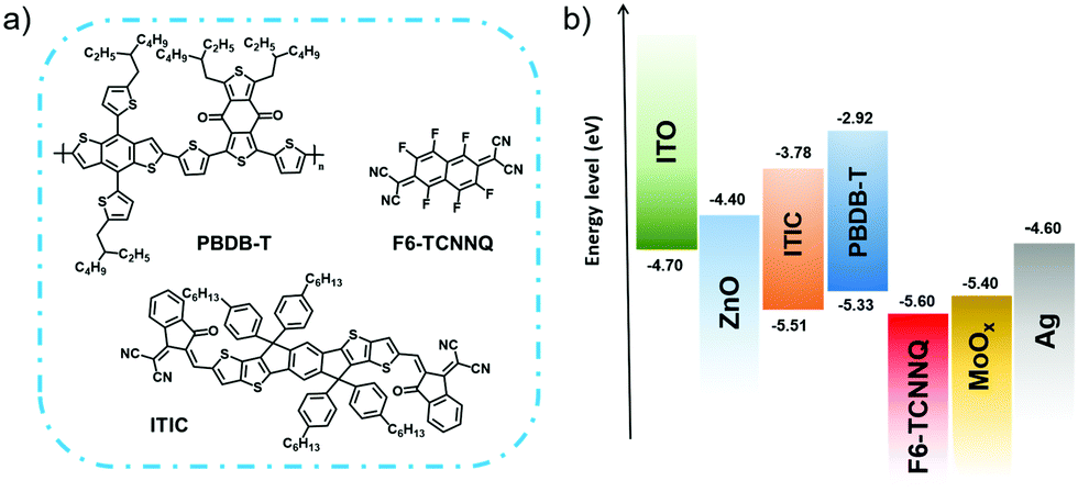 | ||
| Scheme 1 (a) Chemical structures and (b) the energy levels of PBDB-T, ITIC, and F6-TCNNQ. | ||
Experimental section
Materials
PEDOT:PSS was purchased from Heraeus (CLEVIOSTM PVP Al 4083). PBDB-T and ITIC were purchased from Solarmer, Inc (Beijing). F6-TCNNQ was purchased from Lumtec Inc. Glass substrates pre-patterned with indium-tin-oxide (ITO) (sheet resistance = 10 Ω sq−1) were purchased from Southern China City Science and Technology Co., Ltd. All materials were used as received without purification.Device fabrication
Solar cells were fabricated with an inverted structure of ITO/ZnO nanoparticles/active layer/MoOx (F6-TCNNQ)/Ag. ITO-coated glass substrates were sonicated sequentially in detergent, acetone and isopropanol for 15 min, respectively, and then treated in UV-ozone for 15 min. The synthesis of zinc oxide nanoparticles is consistent with previous literature reports.29 A ZnO transporting layer was formed by spin-coating. Afterward, the ZnO coated ITO substrates were transferred into a nitrogen-purged glovebox before use. Solutions of BHJs were prepared by solubilizing PBDB-T and ITIC in chlorobenzene (CB) with a total concentration of 20 mg mL−1 (blend ratio = 1![[thin space (1/6-em)]](https://www.rsc.org/images/entities/char_2009.gif) :1 by weight) added with 0.5% volume of 1,8-diiodooctane (DIO) additives. The solutions were stirred for 3 hours at least at room temperature.
:1 by weight) added with 0.5% volume of 1,8-diiodooctane (DIO) additives. The solutions were stirred for 3 hours at least at room temperature.
Characterization
The current density–voltage (J–V) characteristics of solar cells were measured in a nitrogen-filled glovebox by using a Keithley 2400 Sourcemeter under AM 1.5G irradiation with a solar simulator (70 mm × 70 mm photobeam size) calibrated with a standard silicon reference cell. The EQE was measured by a Solar Cell Spectral Response Measurement System QE-R3011 (Enli Technology Co., Ltd Taiwan). Ultraviolet-visible (UV-Vis) absorption spectra were measured by using a PerkinElmer Lambda 950 spectrometer. Irradiation-dependent solar cell testing was performed by applying a filter wheel with customized optical densities between the samples and the light source to obtain the desired illumination intensities. TPC measurements were performed on customized transient measurement systems (Physike Technology Co., Ltd) by using a pulsed semiconductor laser (488 nm, Coherent, Inc.). Atomic force microscopy (AFM) was performed by using a Bruker Multimode-8 microscope system in tapping mode under ambient conditions. Mott–Schottky analysis was performed by using an electrochemical workstation (CH Instruments, model: CHI660E) in the dark.Results and discussion
The process of the applied sequential doping without MoOx is illustrated in Fig. 1a. The two-step doping was accomplished by first soaking the BHJ film in a low concentration of F6-TCNNQ solution (0.5 mg mL−1), followed by solvent washing with pure IPA to remove the residue of the dopants. After that, F6-TCNNQ solution with a higher concentration (1.5 mg mL−1) was applied on top of the IPA-washed BHJ surface to generate the desired doping effect. For comparison with bulk doping, F6-TCNNQ mixed with the blend of the PBDBT donor and the ITIC acceptor in solution and solid films was obtained by spin-coating the doped BHJ solutions. The current density versus voltage (J–V) characteristics of the solar cells with the two doping methods are shown in Fig. 1b and c (device architectures are illustrated in the insets, accordingly).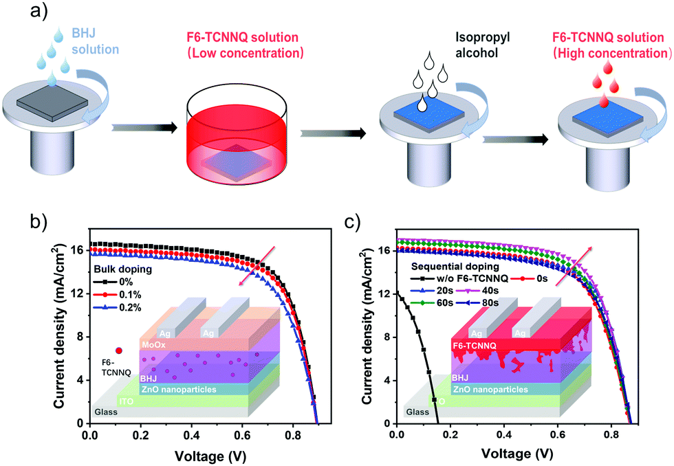 | ||
| Fig. 1 (a) Illustration of the fabrication process for sequential molecular doping devices. (b) and (c) current density versus voltage (J–V) characteristics of the (b) bulk doping and (c) sequential molecular doping devices under AM 1.5G solar irradiation. Inset: Device architecture of the OSCs used in this study. | ||
The detailed parameters of OSCs are summarized in Table 1 and Table S1 (ESI†). The control device containing the MoOx HTL yielded a PCE of 10.01% without doping, showing a JSC of 16.61 mA cm−2, a VOC of 0.89 V and an FF of 0.68. With bulk doping of the device (containing MoOx), we observed a decrease in PCE, even at a low concentration of 0.1% (wt), which is caused by the decrease in JSC and FF. In contrast, with bulk doping the sequentially doped devices (without MoOx) showed an increase in PCE with the increase in the soaking time (up to 40 s), or with useful penetration of dopants (see Table 1). With the best doping conditions (40 s), the PCE reaches ∼10%, which is comparable to that of the control device. However, when we further extend the soaking time (beyond 40 s), the efficiency decreases adversely. This can be caused by the excessive penetration of F6-TCNNQ dopants, approaching the situation of bulk doping. Upon sequential doping (30 s, with MoOx), the PCE can be further boosted to 10.66% with JSC = 16.83 mA cm−2, VOC = 0.89 V and FF = 0.72 (see the results in Fig. S1, ESI†). These results demonstrate that sequentially doped OSCs with F6-TCNNQ work reasonably in the absence of HTLs and also with the combination of the MoOx HTL and with doping, the PCE of our devices can be further improved.
| Doping method | HTL | Doping conditions | V OC (V) | J SC (mA cm−2) | FF (%) | PCE (%) |
|---|---|---|---|---|---|---|
| Bulk doping | MoOx | 0% | 0.89 (0.88 ± 0.01) | 16.61 (16.55 ± 0.17) | 67.71 (66.95 ± 0.99) | 10.01 (9.75 ± 0.19) |
| 0.2% | 0.89 (0.88 ± 0.01) | 15.67 (15.08 ± 0.28) | 65.17 (63.84 ± 2.04) | 9.09 (8.62 ± 0.38) | ||
| Sequential doping | w/o | w/o | 0.16 (0.15 ± 0.01) | 12.67 (12.47 ± 0.30) | 42.09 (41.26 ± 0.10) | 0.85 (0.74 ± 0.07) |
| 40 s | 0.87 (0.86 ± 0.01) | 17.01 (16.90 ± 0.15) | 67.34 (66.34 ± 0.74) | 9.97 (9.68 ± 0.13) |
Previous work has revealed that F4-TCNQ molecules are able to diffuse into organic semiconductor host compounds via a sequential doping process due to their small molecular volume.30,31 To ensure that the large molecule of F6-TCNNQ can penetrate into the active layer to render the desired doping effect, we performed EDX-mapping (see the results in Fig. S2, ESI†). For this measurement, the doped samples were prepared identically to solar cells. Assuming that fluorine is only present in F6-TCNNQ, the F element was used as a fingerprint to assess the presence of dopants. From the results shown in Fig. S3 (in the ESI†), evident EDX signals of the F element are observed in the sequentially doped films for both times of soaking, 30 s and 10 min. This result proves that the F6-TCNNQ molecule indeed diffuses into the bulk phase of PBDBT:ITIC hosts under the described doping conditions. As shown in Fig. 2 we performed the TOF-SIMS test to detect changes in the vertical F6-TCNNQ concentrations. It can be found that for the oxygen element or the nitrogen element contained in BHJ, the curves are substantially coincident. However, the fingerprinted F element has undergone significant changes. For example, with the increase of sputtering time, the signal of F ions visibly decreases, pointing to a decrease of the F6-TCNNQ dopant concentration from the top (surface) region toward the inner parts of the BHJ films. Besides, when we prolong the permeation time for the dopants, the sputtering time required for F to reach the bottom becomes effectively longer, and the F ion content increases. This tendency provides an indication that the F6-TCNNQ penetration depth indeed increases with the soaking time for our sequential doping.
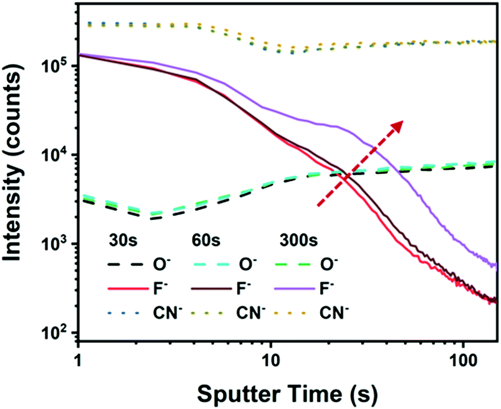 | ||
| Fig. 2 TOF-SIMS profiles of a sequentially doped PBDBT:ITIC BHJ film with F6-TCNNQ dopants. | ||
To assess the surface morphology after doping, we performed atomic force microscopy (AFM), and the topographic AFM and phase images of BHJ films under different doping conditions are shown in Fig. S3 in the ESI.† We observed obvious fibril-like structures in the control film (Fig. S3a, ESI†). To different degrees, the morphology is affected by the applied bulk or sequential doping. For example, even with 0.1% of F6-TCNNQ in the bulk film, the fibril-like structures disappear, showing clusters and prominent white spots. These features are more pronouncedly reflected in the phase images. Advantageously, there are no obvious clusters in the sequentially doped films with 30 s of soaking, while upon increasing the soaking to 10 min, the clusters appear. These results justify that by using the short soaking time for penetration of dopants, damage to the morphology of the BHJ films is reduced, which is the key merit over bulk doping.
The infiltration of the dopants into the photoactive layer is expected to affect the surface electronic properties of the BHJ films. To affirm this, we examined 2D mapping of the surface contact potential (SCP) by scanning Kelvin probe microscopy (see the results in Fig. 3). With the infiltration of the dopants for 30 s (F6-TCNNQ solution concentration = 0.5 mg mL−1), the SCP of the doped BHJ film slightly increases to 4.73 eV, compared to that of the undoped film (4.7 eV). This trend is consistent with the feature of p-doping.32 We also measured the SCP of the Ag top electrode with and without the spin-coating of F6-TCNNQ dopants. As can be seen, the SCP of neat Ag is 4.66 eV, which is smaller with regard to the highest occupied molecular orbital (HOMO) of the PBDBT donor (5.51 eV), and Ag tends to form a non-ohmic contact. After depositing F6-TCNNQ, the SCP (or the work function) of Ag increases to 4.89 eV, getting closer to the HOMO energy of the donor (PBDB-T). By using a higher concentration solution of F6-TCNNQ (1.5 mg mL−1) spin-coated on the surface of BHJ films, the same procedure is used for the 2nd step of sequential doping, and the SCP deepens further (see Fig. S4, ESI†), showing a similar trend with the F6-TCNNQ coated Ag electrode. This modification implies that the hole extraction barrier at the BHJ/Ag interface is mitigated in the presence of F6-TCNNQ, which is beneficial for the device operation.33
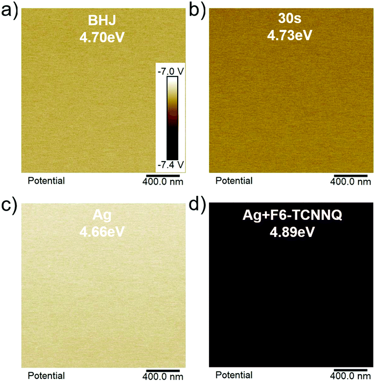 | ||
| Fig. 3 2D mapping of the surface potential attained by scanning Kelvin probe microscopy for (a) the pristine PBDB-T:ITIC BHJ film, (b) the sequentially doped BHJ film with an F6-TCNNQ solution concentration of 0.5 mg mL−1, (c) the freshly evaporated Ag film and (d) and the Ag film spin-coated with F6-TCNNQ solution (conc. = 1.5 mg mL−1). Also provided are the averaged values of the surface contact potential (SCP) of different samples. | ||
Indicated by the results discussed above, the penetration of dopants plays a critical role in the ultimate PCE. In order to explore the influence of dopants on the device performance without MoOx in terms of the device physics, we examined the external quantum efficiencies (EQE) of these solar cells (see Fig. 4a). The photocurrent determined from the integrated EQE is consistent with the values based on J–V characteristics, showing deviations of less than 5%. Compared to the EQE of the control device, the photocurrent of the sequentially doped cells increases in the donor absorption regime (300–700 nm). The largest EQE increase was found with a soaking time of 40 s. Interestingly, the EQE for the ITIC acceptor absorption regime (500–800 nm) also increases with regard to that of the undoped device. From the nearly unaffected absorbance of the sequentially doped photoactive layer at different penetration times (see Fig. S5, ESI†), the increase of EQE cannot be ascribed to the changes of optical absorption but to the synergetic modification of interfacial hole extraction, transport and recombination, as will be further discussed below.
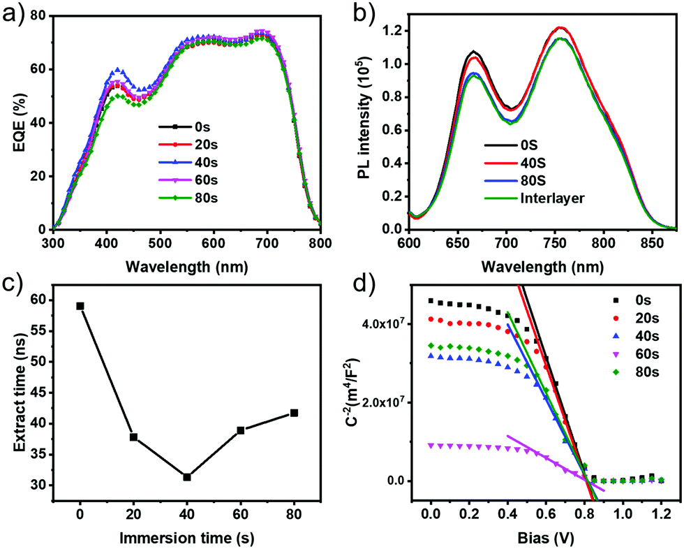 | ||
| Fig. 4 (a) EQE spectra of sequentially doped PBDBT:ITIC solar cells without MoOx. (b) Steady-state photoluminescence (PL) spectra of undoped and F6-TCNNQ doped PBDB-T:ITIC films under different conditions. (c) Charge extraction time in F6-TCNNQ doped OSCs without MoOx as a function of the immersion (or soaking) time for dopants determined by transient photocurrent (TPC) decay measurements. (d) Mott–Schottky plot of capacitance (C) versus voltage (V) of various sequential molecular doping devices without MoOx measured in the dark. | ||
Fig. 4b shows the steady-state photoluminescence (PL) spectra of F6-TCNNQ doped PBDB-T:ITIC films with different penetration of the dopants. For the samples with sequential doping, the PL intensities decrease. Importantly, we note that the dopants’ penetration (or an increase of soaking time) first causes the PL of the PBDB-T donor to reduce, followed by a decrease of the PL of ITIC, seeming to indicate that the penetration of F6-TCNNQ dopants also affects the PL of the ITIC acceptor. To better decouple the effect of the dopants on the PL properties of the two BHJ components, we further measured the PL in the steady-state based on the samples of PBDBT/F6-TCNNQ and ITIC/F6-TCNNQ (see the results in Fig. S6, ESI†). The fluorescence intensities of both the donor and the acceptor decrease upon addition of F6-TCNNQ (0.5%). The reduced PL of the PBDBT donor may be related to the fact that F6-TCNNQ can serve as a PL quencher.34 On this basis, the result of the quenched PL of the donor that occurs earlier seems to point to a vertical phase separation in PBDBT:ITIC BHJ films where the donor components are inclined to distribute in the top area inside the films.35 Such a morphological feature will be beneficial for charge extraction in the device.36 Regarding the reduced PL of the ITIC acceptor in the presence of F6-TCNNQ, we observe an associated red-shift in the PL peak (Fig. S6, ESI†). Apart from the role of F6-TCNNQ as a PL quencher, the introduction of p-dopants into the acceptor phase likely causes an increase of aggregation or impaired crystallinity in ITIC. At this moment, the exact molecular origin is yet to be clarified. The combined results of the PL measurements point to an important fact that introducing p-dopants in NF-BHJ should take into account the possible negative effects on NF-acceptors in terms of the favored molecular stacking or crystallinity in the acceptor domains. In the context of interfacial doping, a delicate control of the penetration of dopants will be of importance for obtaining the desired improvements on photovoltaic efficiencies.
We further performed transient photocurrent (TPC) decay measurements to directly probe charge extraction under device operation conditions (see Fig. 4c and Fig. S7, ESI†). The determined charge extraction time (τextr) was found to decrease with the increase of penetration time up to 40 s with a value of τextr = 31.34 ns, versus a τextr of 59.08 ns without doping. This indicates that the most efficient carrier sweep-out with minimized recombination losses is achieved under these doping conditions, which agrees with the enhanced JSC and FF. With a further increase in the penetration time (to 80 s), τextr adversely increases and in the TPC device traces (Fig. S7, ESI†) pronounced long-decay tails are observed. These observations can be ascribed to the trap states formed in the doped films with excess dopant penetration. At this moment, the microscopic origins for the doping-induced trapping are not fully understood, while they may be related to the disturbance in the morphology or inhomogeneity of carrier distribution.37
In order to study the effect of dopant penetration on charge recombination, we performed solar cell characterization under different irradiation intensities (Plight). The slope of the JSCversus Plight characteristics slightly enlarges approaching 1 with increased penetration time (see Fig. S8a and Table S2 in the ESI†). It appears that in these sequentially doped devices, monomolecular recombination is dominant under short-circuit conditions.38 The slope of the characteristics of VOCvs. Plight provides information on the recombination mechanisms (under open-circuit conditions) with the slope = thermal voltage (kBT/q) and the one larger than kBT/q pointing to the dominating bimolecular recombination and the role of Shockley–Read–Hall (SRH) type recombination, respectively.39 As shown in Fig. S8b and Table S1 in the ESI,† the slope does not change significantly in the devices with short-time dopant infiltration, while the slope begins to deviate from unity when the penetration exceeds 40 s. This result fully agrees with the TPC measurements that with appropriate control of dopant penetration, the type of recombination is hardly affected, while long-time penetration tends to cause increased charge trapping and resultant SRH recombination which can impair the device performance.
Bulk doping of OSCs with F4-TCNQ has been found to increase the carrier concentration (Nd), which is used to explain the enhanced carrier transport.12,13 To verify whether the applied sequential doping induces similar effects, or not, we estimated Nd for these sequentially doped devices without MoOx based on the Mott–Schottky plot shown in Fig. 4d. The extracted Nd amounts to 6.81 × 1020 cm−3 in the undoped device and it linearly increases with the penetration of dopants, reaching 3.63 × 1021 cm−3 for the 60 s-soaked device (see Table 2). In the presence of excess background charges in the semiconductor layer, the width of the depletion region can be narrowed.40 As such, there will be a very thin space-charge layer to facilitate charge injection through tunneling.41 With the enlargement of Nd, the interfacial properties at BHJ/Ag and hole extraction are improved, which agrees with the results of TPC. We further examined the carrier transport properties of these sequentially doped BHJ films by single-carrier device measurements (see Fig. S9, ESI†). The extracted mobility for the two carriers is summarized in Table 2. As can be seen, there is a slight enhancement of the hole mobility (μh) with the penetration of F6-TCNNQ, reaching 2.87 × 10⁻⁴ cm2 V−1 s−1 upon soaking for 40 s. Meanwhile, we found that in the devices with weak penetration of dopants, the electron mobility (μe) is affected insignificantly, while μe tends to reduce with the penetration time exceeding 40 s, probably related to the poor molecular order or doping-induced morphology traps.10,37 Importantly, under the optimal doping conditions (40 s), the best mobility balance between the two carriers is realized, displaying a mobility ratio (μh/μe) of 0.78, compared to 0.70 for the undoped device. Our transport study coupled with the results of transient analysis suggests that by controlling the penetration of dopants, the transport balance and interfacial charge extraction can be simultaneously improved which helps suppress the unfavorable space-charge effect and recombination losses, such that the JSC and FF are improved in the solar cell.
| Doping condition (s) | μ h (cm2 V−1 s−1) | μ e (cm2 V−1 s−1) | N d (cm−3) |
|---|---|---|---|
| 0 | 2.55 × 10⁻⁴ | 3.63 × 10⁻⁴ | 6.81 × 10²⁰ |
| 20 | 2.54 × 10⁻⁴ | 3.66 × 10⁻⁴ | 7.17 × 10²⁰ |
| 40 | 2.87 × 10⁻⁴ | 3.69 × 10⁻⁴ | 1.06 × 10²¹ |
| 60 | 2.78 × 10⁻⁴ | 3.51 × 10⁻⁴ | 3.63 × 10²¹ |
| 80 | 2.53 × 10⁻⁴ | 3.04 × 10⁻⁴ | 9.79 × 10²⁰ |
Conclusion
We report a sequential doping approach with F6-TCNNQ as a p-dopant for non-fullerene OSCs to realize modulated charge extraction, transport and ultimate photovoltaic efficiency. Compared to the commonly adopted bulk doping, we showed that the sequential doping process effectively suppresses dopant-induced aggregations in BHJ films, a critical concern for applying bulk molecular doping to OSCs. Due to the strong electron-withdrawing capability, the penetrated F6-TCNNQ dopants greatly promote hole injection/extraction at the anode, such that the solar cells can be operated adequately without using hole transporting layers. By controlling the penetration of the dopants via the soaking time, the doped devices yields PCEs that are comparable to the efficiencies of the MoOx based devices. Investigations with transient electrical analysis and steady-state transport measurements indicate that the adopted sequential doping mainly affects the density of background charges in the solar cell and the interfacial properties at BHJ/Ag. As a result, enhanced charge extraction with reduced recombination losses is achieved. To realize a universal doping strategy for polymer donors with deeper-lying HOMO levels, which potentially can increase the VOC, efforts on seeking novel molecular dopants may be made toward wider windows for tuning of charge extraction and electrode WF.Conflicts of interest
There are no conflicts to declare.Acknowledgements
This work was supported by the National Natural Science Foundation of China (No. 21875012 and 21674006). H. Zhou acknowledges the financial support from the National Natural Science Foundation of China (NSFC) (No. 21773045), the National Key Research and Development Program of China (2017YFA0206600), and the Chinese Academy of Science (100 Top Young Scientists Program). Y. Z. thanks the “111” Project.Notes and references
- S. Dong, K. Zhang, B. Xie, J. Xiao, H.-L. Yip, H. Yan, F. Huang and Y. Cao, Adv. Energy Mater., 2019, 9, 1802832 CrossRef
.
- M. Kaltenbrunner, M. S. White, E. D. Głowacki, T. Sekitani, T. Someya, N. S. Sariciftci and S. Bauer, Nat. Commun., 2012, 3, 770 CrossRef PubMed
- L. Yang, T. Zhang, H. Zhou, S. C. Price, B. J. Wiley and W. You, ACS Appl. Mater. Interfaces, 2011, 3, 4075–4084 CrossRef CAS PubMed
- L. Gomez De Arco, Y. Zhang, C. W. Schlenker, K. Ryu, M. E. Thompson and C. Zhou, ACS Nano, 2010, 4, 2865–2873 CrossRef CAS
- Y. Lin, J. Wang, Z.-G. Zhang, H. Bai, Y. Li, D. Zhu and X. Zhan, Adv. Mater., 2015, 27, 1170–1174 CrossRef CAS
- Y. Lin and X. Zhan, Mater. Horiz., 2014, 1, 470–488 RSC
- Y. Cui, H. Yao, J. Zhang, T. Zhang, Y. Wang, L. Hong, K. Xian, B. Xu, S. Zhang, J. Peng, Z. Wei, F. Gao and J. Hou, Nat. Commun., 2019, 10, 2515 CrossRef
- X. Xu, K. Feng, Z. Bi, W. Ma, G. Zhang and Q. Peng, Adv. Mater., 2019, 31, 1901872 CrossRef
- K. Li, Y. Wu, Y. Tang, M.-A. Pan, W. Ma, H. Fu, C. Zhan and J. Yao, Adv. Energy Mater., 2019, 9, 1901728 CrossRef
- J. Wang, Z. Zheng, D. Zhang, J. Zhang, J. Zhou, J. Liu, S. Xie, Y. Zhao, Y. Zhang, Z. Wei, J. Hou, Z. Tang and H. Zhou, Adv. Mater., 2019, 31, 1806921 CrossRef
- V. C. Nikolis, A. Mischok, B. Siegmund, J. Kublitski, X. Jia, J. Benduhn, U. Hörmann, D. Neher, M. C. Gather, D. Spoltore and K. Vandewal, Nat. Commun., 2019, 10, 3706 CrossRef
- Y. Zhang, H. Q. Zhou, J. Seifter, L. Ying, A. Mikhailovsky, A. J. Heeger, G. C. Bazan and T. Q. Nguyen, Adv. Mater., 2013, 25, 7038–7044 CrossRef CAS
- Y. Xiong, L. Ye, A. Gadisa, Q. Zhang, J. J. Rech, W. You and H. Ade, Adv. Funct. Mater., 2019, 29, 1806262 CrossRef
- H. Yan, J. Chen, K. Zhou, Y. Tang, X. Meng, X. Xu and W. Ma, Adv. Energy Mater., 2018, 8, 1703672 CrossRef
- R. Wang, D. Zhang, S. Xie, J. Wang, Z. Zheng, D. Wei, X. Sun, H. Zhou and Y. Zhang, Nano Energy, 2018, 51, 736–744 CrossRef CAS
- X. Zhou, J. Blochwitz, M. Pfeiffer, A. Nollau, T. Fritz and K. Leo, Adv. Funct. Mater., 2001, 11, 310–314 CrossRef CAS
- J. Soeda, Y. Hirose, M. Yamagishi, A. Nakao, T. Uemura, K. Nakayama, M. Uno, Y. Nakazawa, K. Takimiya and J. Takeya, Adv. Mater., 2011, 23, 3309–3314 CrossRef CAS PubMed
- M. K. Fung, K. M. Lau, S. L. Lai, C. W. Law, M. Y. Chan, C. S. Lee and S. T. Lee, J. Appl. Phys., 2008, 104, 034509 CrossRef
- I. E. Jacobs, E. W. Aasen, J. L. Oliveira, T. N. Fonseca, J. D. Roehling, J. Li, G. Zhang, M. P. Augustine, M. Mascal and A. J. Moulé, J. Mater. Chem. C, 2016, 4, 3454–3466 RSC
- J. Li, G. Zhang, D. M. Holm, I. E. Jacobs, B. Yin, P. Stroeve, M. Mascal and A. J. Moulé, Chem. Mater., 2015, 27, 5765–5774 CrossRef CAS
- Y. Zhang, B. de Boer and P. W. M. Blom, Adv. Funct. Mater., 2009, 19, 1901–1905 CrossRef CAS
- D. T. Duong, C. Wang, E. Antono, M. F. Toney and A. Salleo, Org. Electron., 2013, 14, 1330–1336 CrossRef CAS
- J. Gao, J. D. Roehling, Y. Li, H. Guo, A. J. Moulé and J. K. Grey, J. Mater. Chem. C, 2013, 1, 5638–5646 RSC
- L. Ye, H. Hu, M. Ghasemi, T. Wang, B. A. Collins, J.-H. Kim, K. Jiang, J. H. Carpenter, H. Li, Z. Li, T. McAfee, J. Zhao, X. Chen, J. L. Y. Lai, T. Ma, J.-L. Bredas, H. Yan and H. Ade, Nat. Mater., 2018, 17, 253–260 CrossRef CAS
- L. Arunagiri, G. Zhang, H. Hu, H. Yao, K. Zhang, Y. Li, P. C. Y. Chow, H. Ade and H. Yan, Adv. Funct. Mater., 2019, 29, 1902478 CrossRef
- I. E. Jacobs, C. Cendra, T. F. Harrelson, Z. I. Bedolla Valdez, R. Faller, A. Salleo and A. J. Moulé, Mater. Horiz., 2018, 5, 655–660 RSC
- V. A. Kolesov, C. Fuentes-Hernandez, W.-F. Chou, N. Aizawa, F. A. Larrain, M. Wang, A. Perrotta, S. Choi, S. Graham, G. C. Bazan, T.-Q. Nguyen, S. R. Marder and B. Kippelen, Nat. Mater., 2016, 16, 474 CrossRef
- F. Zhang and A. Kahn, Adv. Funct. Mater., 2018, 28, 1703780 CrossRef
- X. Zhang, S. Yang, S. Bi, A. Kumaresan, J. Zhou, J. Seifter, H. Mi, Y. Xu, Y. Zhang and H. Zhou, RSC Adv., 2017, 7, 12400–12406 RSC
- F. Guillain, J. Endres, L. Bourgeois, A. Kahn, L. Vignau and G. Wantz, ACS Appl. Mater. Interfaces, 2016, 8, 9262–9267 CrossRef CAS PubMed
- J. Li, C. W. Rochester, I. E. Jacobs, S. Friedrich, P. Stroeve, M. Riede and A. J. Moulé, ACS Appl. Mater. Interfaces, 2015, 7, 28420–28428 CrossRef CAS PubMed
- M. L. Tietze, L. Burtone, M. Riede, B. Lüssem and K. Leo, Phys. Rev. B: Condens. Matter Mater. Phys., 2012, 86, 035320 CrossRef
- L. Lu, T. Xu, I. H. Jung and L. Yu, J. Phys. Chem. C, 2014, 118, 22834–22839 CrossRef CAS
- P. Tyagi, S. Tuli and R. Srivastava, J. Phys. Chem., 2015, 142, 054707 CrossRef
- P. Bi, T. Xiao, X. Yang, M. Niu, Z. Wen, K. Zhang, W. Qin, S. K. So, G. Lu, X. Hao and H. Liu, Nano Energy, 2018, 46, 81–90 CrossRef CAS
- Y. Bai, B. Yang, C. Zhao, Z. Shi, T. Hayat, A. Alsaedi and Z. a. Tan, J. Mater. Chem. A, 2018, 6, 7257–7264 RSC
- V. I. Arkhipov, P. Heremans, E. V. Emelianova and H. Bässler, Phys. Rev. B: Condens. Matter Mater. Phys., 2005, 71, 045214 CrossRef
- S. Xie, Y. Xia, Z. Zheng, X. Zhang, J. Yuan, H. Zhou and Y. Zhang, Adv. Funct. Mater., 2018, 28, 1705659 CrossRef
- S. R. Cowan, A. Roy and A. J. Heeger, Phys. Rev. B: Condens. Matter Mater. Phys., 2010, 82, 245207 CrossRef
- J. Blochwitz, T. Fritz, M. Pfeiffer and K. Leo, Org. Electron., 2001, 2, 97–104 CrossRef CAS
- B. Lüssem, C.-M. Keum, D. Kasemann, B. Naab, Z. Bao and K. Leo, Chem. Rev., 2016, 116, 13714–13751 CrossRef
Footnote |
| † Electronic supplementary information (ESI) available: Supporting figures and notes. See DOI: 10.1039/c9tc04969j |
| This journal is © The Royal Society of Chemistry 2020 |