
Chemical understanding of resistance drift suppression in Ge–Sn–Te phase-change memory materials†
Yuhan
Chen‡
a,
Liang
Sun‡
*b,
Yuxing
Zhou
a,
Getasew M.
Zewdie
a,
Volker L.
Deringer§
 c,
Riccardo
Mazzarello
d and
Wei
Zhang
*ae
c,
Riccardo
Mazzarello
d and
Wei
Zhang
*ae
aCenter for Advancing Materials Performance from the Nanoscale, State Key Laboratory for Mechanical Behavior of Materials, Xi’an Jiaotong University, Xi’an 710049, China
bKey Laboratory of Materials Processing Engineering, College of Materials Science and Engineering, Xi'an Shiyou University, Xi'an 710065, China. E-mail: lsun@xsyu.edu.cn
cDepartment of Engineering, University of Cambridge, Cambridge CB2 1PZ, UK
dInstitute for Theoretical Solid-State Physics, JARA-FIT and JARA-HPC, RWTH Aachen University, Aachen 52056, Germany
eXi'an Jiaotong University Suzhou Institute, Suzhou 215123, China. E-mail: wzhang0@mail.xjtu.edu.cn
First published on 11th November 2019
Abstract
The resistance drift phenomenon observed in amorphous chalcogenide phase-change materials (PCMs) hinders the development of PCM-based neuro-inspired computing devices. It has been observed that the drift in electrical resistance can be effectively reduced by substituting Ge with Sn in the prototype PCM GeTe, forming amorphous (Ge1−xSnx)Te solids. However, the atomistic and chemical origin of such drift suppression phenomenon remains unclear. In this work, we carry out thorough ab initio simulations and chemical bonding analyses of amorphous Ge–Sn–Te materials. We show that the two critical driving forces for glass relaxation in PCMs, i.e. the amount of tetrahedral motifs and the degree of Peierls distortion, are gradually reduced as Sn content increases. Such trend can be explained by the increased ionicity brought about by the Ge → Sn substitution. Our work suggests that an optimal Sn-rich GeSnTe composition could be reached for PCM-based neuro-inspired computing with ultralow resistance drift.
Chalcogenide phase-change materials (PCMs)1–10 hold great promise in response to the rapidly growing demand on data storage and processing, driven by artificial intelligence and other data-intensive applications. The recently released PCM-based nonvolatile memory products11 significantly improve the computing efficiency of supercomputers by bridging the performance gap between solid-state hard drive (SSD) and dynamic random access memory (DRAM). Even more importantly, PCM-based memory cells can be assembled into devices resembling neural networks through crossbar arrays, which can carry out direct arithmetic computation, logic operation and even machine-learning tasks in memory units.12–18 Such scheme is known as neuro-inspired computing, which, in principle, is fundamentally more efficient in power and computing than conventional von Neumann devices, because massive and extensive data transfer between multiple processing and memory units is no longer required.12–18
Phase-change memory exploits rapid and reversible phase transitions between the amorphous and crystalline states of PCMs for switching, where SET and RESET operations correspond to crystallization and amorphization, respectively.1 The large contrast in electrical resistance is used to identify the binary logic state “0”—high-resistance amorphous state, and “1”—low-resistance crystalline state.1 The resistance contrast in GeTe and Ge2Sb2Te5 compounds is over 3–6 orders of magnitude,19 and it is feasible to generate multiple intermediate resistance states by tuning the amorphous—crystalline ratio in a single memory cell.20 Such programming scheme is known as iterative RESET, which serves as a key element for phase-change neuro-inspired computing.21 However, amorphous PCMs typically undergo spontaneous structural relaxation at room temperature,22–24 resulting in the resistance drift phenomenon: the cell resistance increases steadily with time,25 limiting the accuracy and efficiency of neuro-inspired computing using PCM arrays.21 With applications of PCMs envisioned to move from binary data storage to neuro-inspired computing, strategies for reducing and eventually avoiding resistance drift are an important research target.
For amorphous PCMs, the change of resistance obeys the power law, R(t) = R0(t/t0)v, where R0 is the initial resistance at t0, and v is the drift coefficient.25 The initial cell resistance of a typical Ge2Sb2Te5 device is ∼106 Ω in its RESET state and ∼103 Ω in its SET state. The SET resistance remains nearly unchanged with time, while the RESET resistance, with a drift coefficient of 0.11,25 shows an increase of ∼3 × 10⁶ Ω over ∼1 hour at room temperature.25 Thus, the resistance value of a given intermediate state may enter the resistance window of its adjacent state within minutes, triggering decoding errors. In parallel to device programming and fabrication strategies26–28 that circumvent the resistance drift issue partly, composition engineering29 and heterostructure design30 were employed to reduce the drift coefficient of amorphous PCMs. Among various alloying elements, Sn was shown to improve the crystallization performance31,32 and reduce the drift coefficient:33,34 at 50 °C, v of amorphous GeTe was measured as ∼0.129, which was reduced to ∼0.095 with 25% Sn substitution (Ge3SnTe4), and to ∼0.053 with 50% Sn substitution (GeSnTe2). However, the underlying atomic-scale mechanisms have not been fully clarified.
Here, we elucidate the atomic origin of the reduction in drift coefficient by performing thorough structural characterizations and chemical bonding analyses of amorphous GeTe, GeSnTe2 and SnTe, based on ab initio simulations. All three amorphous compounds were simulated using ab initio molecular dynamics (AIMD) via a melt-quench procedure, and ten independent models with different thermal history were considered for each compound to obtain better statistics (see Methods). Each model contained 216 atoms, which were initially placed in a cubic box with the corresponding theoretical amorphous density for GeTe, GeSnTe2 and SnTe, respectively. Three typical amorphous configurations are shown in Fig. 1a. Analysis of the structures shows that long-range order is absent and elemental phase segregation is not observed. We performed self-consistent calculations and chemical bonding analyses based on the amorphous configurations relaxed at zero K to assess their electronic structures and bonding characteristics (see Methods). We employed the crystal orbital overlap population (COOP)35 method, based on a projection scheme for the electronic wavefunctions, to investigate the covalent interactions in amorphous GeSnTe2 and SnTe, in direct comparison with our previous work on amorphous GeTe.36 In addition, we analyzed atomic charges in the same theoretical framework to assess the electrostatic nature of the three amorphous compounds.
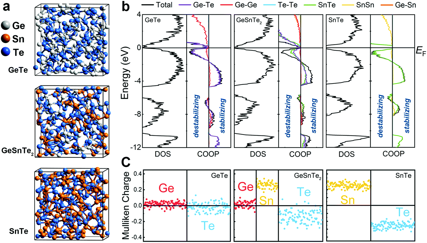 | ||
| Fig. 1 (a) Snapshots of amorphous GeTe, GeSnTe2 and SnTe generated by AIMD simulations. The Ge, Sn and Te atoms are rendered with grey, orange and blue spheres. (b) The density of states (DOS) and projected crystal orbital overlap populations (COOP) curves of the three amorphous compounds. (c) The Mulliken charges (in electrons per atom) of all atoms in the three amorphous compounds. | ||
All three amorphous compounds show a narrow band gap below 1 eV, and a few mid-gap states can be observed in amorphous GeTe and GeSnTe2, as evidenced by the electronic density of states (DOS) shown in Fig. 1b. The observation of mid-gap states is in line with modulated photocurrent experiments carried out on amorphous GeTe and GeSnTe2 thin films.33,34 The corresponding COOP plots show that large energy regions below the Fermi level EF are dominated by bonding interactions for all three amorphous compounds. The presence of a finite antibonding region right below EF does not lead to significant structural rearrangement at zero K. In fact, such antibonding feature is also observed in crystalline GeTe36 and other PCMs.37–39 COOP analyses indicate that both bonding and antibonding interactions below EF are contributed by heteropolar bonds in the three amorphous compounds (Fig. 1b).
Despite the similar DOS and COOPs in the three amorphous compounds, a qualitative difference is observed in their respective electrostatic character. Mulliken charge analyses in Fig. 1c show that Ge atoms and Te atoms are almost charge-neutral (only slightly positively and negatively charged, respectively) in amorphous GeTe, while a larger charge transfer between Sn and Te atoms is found in amorphous SnTe, in line with the respective crystals (Fig. S1, ESI†). In amorphous GeSnTe2, the Mulliken charges of Ge and Sn atoms are similar to the respective values in amorphous GeTe and SnTe, while the Mulliken charges of Te atoms span a wider range. The degree of charge transfer in these Te atoms depends on the neighboring configuration, i.e. the more Sn neighbors, the larger the charge transfer (Fig. S2, ESI†). The gradual increase in charge transfer or ionicity brought by Sn substitution leads to a larger energy penalty for forming homopolar bonds; therefore, the amorphous network of SnTe is more ordered than that of GeTe in terms of local fluctuations in chemical composition.
The increased order in the Sn-richer amorphous networks becomes more evident with structural analyses as resolved according to individual atomic species. All data shown below were collected over 10 models for each compound. Except for the bonding data that were obtained at zero K, other structural data were obtained at 300 K over 20 ps. The total and partial radial distribution function g(r) of the three amorphous compounds are shown in Fig. 2. The first peak position of Ge–Te and Sn–Te bonding pairs is at 2.76 Å and 3.05 Å, respectively. These heteropolar bonds dominate the respective amorphous networks, and lead to a flattened first peak in the total g(r) of GeSnTe2. As regards the (quasi-) homopolar bonds, a clear peak is observed at 2.65 Å for Ge–Ge bonds in GeTe and GeSnTe2, a small peak at 2.86 Å for Ge–Sn bonds in GeSnTe2, a shoulder at around ∼3.30 Å for Sn–Sn bonds in GeSnTe2 and SnTe, while Te–Te bonds below 3.5 Å are nearly absent in all three amorphous compounds. In GeSnTe2, both Ge and Sn are cation-like atoms with positive charges, thus the Ge–Sn bonds are considered to be “quasi-homopolar” bonds.
 | ||
| Fig. 2 (a) The total and partial radial distribution functions g(r) and the distribution of bond populations BAB of amorphous GeTe, GeSnTe2 and SnTe. (b) The bond-weighted distribution functions (BWDF) of the three amorphous compounds. The crossover positions from bonding to antibonding interaction can be regarded as the cutoffs for chemical bonds in the respective amorphous networks. | ||
As a more direct measure of the strength of chemical bonds, the bond population can be calculated by integrating COOP(E) along the energy axis, up to EF (that is, over all occupied bands), for a specific pair of atoms A and B, viz. . Interatomic contacts up to 7 Å were considered: the range of our analysis is therefore much longer than typical covalent bond lengths, to gain a more comprehensive picture. As shown in Fig. 2a, the bond population decreases as the interatomic distance increases for both heteropolar and homopolar bonds, and a crossover from bonding to antibonding interaction (as assessed here by the integration of COOP) appears at distances above 3 Å in all three amorphous compounds. At even larger distances, the interactions tend toward zero, as expected (due to the lack of substantial orbital overlap). As developed in our previous work,36 a “bond-weighted distribution function” (BWDF) given by the multiplication between the bond population and g(r),
  , provides a simple and intuitive measure for bonding patterns in amorphous networks. The element-resolved BWDFs presented in Fig. 2 show a crossover from bonding to antibonding character in Ge–Ge and Ge–Te contacts for the compounds GeTe and GeSnTe2 at 3.05 Å and 3.16 Å, respectively. The Sn–Te interactions are classified as bonding up to 3.36 Å, both in GeSnTe2 and SnTe, and the quasi-homopolar Ge–Sn bonds are identified at up to 3.27 Å in GeSnTe2. Te⋯Te interatomic contacts are mostly repelling and occur at above 3.5 Å: there is no covalent Te–Te bonding in these materials, as noted before. As regards Sn–Sn bonds, very little bonding interaction can be found in GeSnTe2 and SnTe, and a crossover at 3.47 Å is observed. There is, hence, a qualitative difference between the behavior of Ge atoms and that of Sn atoms in these compounds.
These distance values were then used as cutoffs for defining bonded contacts (and obtaining coordination numbers) in these amorphous networks, giving access to further structural analyses. First, we quantify the ratio of homopolar bonds in the three amorphous compounds, and a systematic reduction of homopolar bonds is observed from 13.0% (±0.8%) in GeTe, to 8.8% (±0.9%) in GeSnTe2 and to 4.8% (±1%) in SnTe. This trend stems from the increased ionicity upon Sn substitution as discussed above. Second, the average coordination number (CN) of both Ge and Sn atoms in the three amorphous compounds is found to be around 4, while that of Te atom gets increased as the concentration of Sn increases (Fig. 3a). Third, the angular distribution functions show that the bond angles around Te and Sn atoms are close and slightly smaller than 90°, while Ge atoms tend to have larger bond angles shifted towards 100°. As measured by the bond order parameter  between atoms A, B and C, tetrahedral motifs around the center atom B, denoted by BT, are defined by q > 0.8, four-fold defective octahedral BO are indicated by a value of q of approximately 5/8. The two typical motifs are visualized in Fig. 3a.
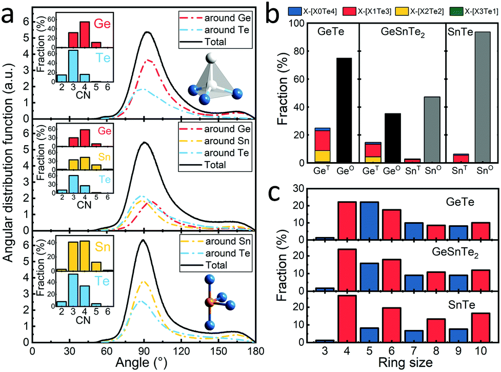 | ||
| Fig. 3 (a) The angular distribution functions and coordination number (CN) distribution of amorphous GeTe, GeSnTe2 and SnTe. Two typical local motifs in amorphous GeTe and SnTe are shown as insets, i.e. a tetrahedral Ge motif with one homopolar bond and a four-fold defective octahedral Sn motif with all heteropolar bonds. (b) The fraction of tetrahedral XT and four-fold defective octahedral XO motifs in the three amorphous compounds. (c) The fraction of primitive rings in the three amorphous compounds. | ||
It was concluded in ref. 22 that, during the structural relaxation or aging of amorphous GeTe, (i) the vanishing of tetrahedral motifs reduces the density of mid-gap states and (ii) the reinforcement of Peierls distortion in defective octahedral motifs widens the band gap,22 which together result in a steady increase in electrical resistance. Here we show that these two driving forces for aging are both effectively reduced upon Sn substitution, giving rise to the suppression of the drift coefficient. As shown in Fig. 3b, the fraction of tetrahedral motifs is reduced from ∼27% to ∼7% from GeTe40,41 to SnTe, and the vast majority of the tetrahedral motifs is stabilized by homopolar Ge–Ge or Sn–Sn bonds in GeTe and SnTe, which were formed during the rapid quenching process. Tetrahedral motifs made of pure heteropolar bonds, which we indicate by writing the coordination shell in square brackets as GeT[Ge0Te4] or SnT[Sn0Te4], respectively, are rarely found in all three amorphous compounds. This is consistent with the fact that no comparable coordination environment is found in crystalline polymorphs of either compound.22,42 A strongly antibonding interaction near EF was found for the SnT[Sn0Te4] motifs but not for the SnT[Sn1Te3] motifs in amorphous SnTe (Fig. S3, ESI†), in line with the observation for amorphous GeTe.36 Our present results thereby indicate that despite somewhat larger atomic charges in SnTe, the fundamental chemical bonding mechanisms in both amorphous PCMs follow similar principles. The reduction in homopolar bonds and thereby tetrahedral motifs in Sn-rich amorphous systems is reflected by the difference in the heat of formation of the crystals, i.e. −48.7 kJ mol−1 for GeTe43 and −61.1 kJ mol−1 for SnTe,44 indicating an increased energy penalty for forming homopolar bonds upon moving from GeTe to SnTe. As mentioned above, tetrahedral motifs give rise to mid-gap states in amorphous GeTe,22 and the vanishing of these motifs with time serves as one of the two major causes of aging in amorphous GeTe22,45 and Ge2Sb2Te5.46 Upon Sn substitution, the concentration of tetrahedral motifs decreases sharply, giving rise to the reduced density of mid-gap states33 and thereby smaller driving force for aging.
Peierls distortion is typically found in crystalline PCMs and other semiconductors: such symmetry-lowering distortion leads to the formation of long and short bonding pairs and a widening of the band gap. In the amorphous phase, Peierls-like distortions can be quantified by calculating the bond distribution over bonding pairs with an angle close to 180°, termed as angular-limited three-body correlation (ALTBC, normalized per atom).22 As shown in Fig. 4, GeTe shows a strong correlation of short-long bonding pattern with a peak at 2.8/3.5 Å, while the bond distribution is more centralized around 3.3 Å in SnTe. In GeSnTe2, the bond distribution is a mixture of the bonding patterns of GeTe and SnTe, and element-resolved ALTBCs clearly distinguish the distortion-pronounced Ge motifs from the more uniformly bonded Sn motifs. Two typical motifs around Ge and Sn atoms in GeSnTe2 are shown in Fig. 4d. These analyses show a trend towards suppression of Peierls distortion when Sn content gets rich. This behavior is also reflected in the respective crystalline counterparts, in that GeTe shows a much stronger Peierls distortion with 2.86/3.25 Å bonding pattern than SnTe with 3.14/3.27 Å at zero K (Fig. S1, ESI†). At room temperature, SnTe is known to form a perfect rocksalt structure with no Peierls distortion.47 Therefore, the much weaker Peierls distortion in Sn–Te is expected to have a smaller impact on glass relaxation as compared to Ge–Te.
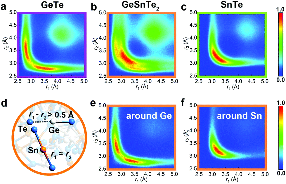 | ||
| Fig. 4 (a)–(c) The bond distributions in amorphous GeTe, GeSnTe2 and SnTe are analyzed by the angular-limited three-body correlation (ALTBC, normalized per atom). A strong short-long bond correlation is found in amorphous GeTe, and gets decreased upon Sn substitutions. The ALTBC near the upper-right corner is mostly contributed by Ge/Sn–Te–Ge/Sn contacts with large bond distances. (d) A snapshot of a local configuration in amorphous GeSnTe2 obtained from our simulations, where large Peierls-like distortion is found around Ge atoms, but not around Sn atoms. (e) and (f) The bond distributions around Ge and Sn atoms in amorphous GeSnTe2. | ||
From another perspective, the dissimilarity in local motifs between the amorphous and crystalline phase is less pronounced in SnTe, implying smaller energy barriers for crystallization upon tuning the stoichiometry from GeTe to SnTe. Indeed, the crystallization temperature of GeTe thin films of ∼180 °C decreases to 120 °C for GeSnTe2 thin films.33 Regarding SnTe, it crystallizes spontaneously at room temperature, and the crystallization temperature of thin films was measured to be around −90 °C,48 making the pure binary phase less suitable for PCM applications. Our medium-range order analyses through the primitive ring statistics shed light on the structural origin of this crystallization tendency. As shown in Fig. 3c, the odd-membered rings, in particular 5-membered ones, are abundant in GeTe due to the presence of relatively large amounts of homopolar bonds.40,49 Upon Sn substitution, odd-fold rings are largely reduced due to the increased energy penalty for homopolar bonds, turning the amorphous networks to resemble their crystalline counterparts more closely. The four-fold rings with ABAB alternation (A = Ge or Sn, B = Te) represent the smallest crystalline unit of the recrystallized phase, and its ratio increases from ∼91% in amorphous GeTe to ∼99% in amorphous SnTe (Fig. S4, ESI†) due to the larger energy penalty of homopolar bonds upon Sn substitution. Note that, for neuro-inspired computing, non-volatility over decades is no longer a stringent parameter: in fact, short-term storage over hours at room temperature is already sufficient for most neuro-inspired computing tasks.21,50,51 Therefore, the decrease in amorphous stability upon partial Sn substitution is not a major problem for neuro-inspired computing applications, whereas the improved crystallization speed and reduced drift coefficient should boost their accuracy and efficiency.
In summary, we carried out thorough structural and bonding analyses of amorphous GeTe, GeSnTe2 and SnTe, based on ab initio simulations, and attributed the suppression of resistance drift in Sn-rich PCMs to the much reduced structural driving forces for glass relaxation upon Sn substitution. We suggest that by engineering the stoichiometry of GexSn(1−x)Te (x < 0.5) towards Sn-rich compositions, it is possible to find an optimized balance between ultralow drift (towards 0.005 and below) at room temperature yet high speed of phase transitions for memory operations. The resistance contrast window in such compound should be sufficiently large to accommodate multiple intermediate resistance states, as the sheet resistance value changes over three to four orders of magnitude in both SnTe48 and GeTe19 thin films upon crystallization. Thus, we propose that Sn-rich Ge–Sn–Te compounds could be a suitable candidate for high-performance phase-change neuro-inspired chips.
Methods
Ab initio molecular dynamics simulations were carried out using the second-generation Car–Parrinello scheme,52 as implemented in the CP2K package.53 The Kohn–Sham orbitals were expanded in basis sets with double- and triple-zeta plus polarization quality, whereas plane waves with a cutoff of 300 Ry were used to expand the charge density. Goedecker pseudopotentials54 and the Perdew–Burke–Ernzerhof (PBE) functional55 were employed. The Brillouin zone was sampled at the k = Γ point, as is common in computational studies of this type. Canonical ensemble (NVT) with a stochastic Langevin thermostat was used. The time step was 2 fs. Amorphous GeTe, GeSnTe2 and SnTe were generated following a melt-quench procedure. They were randomized at above 2000 K and were quenched down to 1000 K for equilibration over 30 ps. The molten liquids were then quenched down to 300 K within 50 ps and were equilibrated at 300 K for 30 ps. All systems were cooled down to zero K for further relaxation, prior to the electronic structure calculations and chemical bonding analyses. Each model contained 216 atoms that were placed in a cubic box with a lattice parameter of 18.9, 19.45 or 19.95 Å for GeTe, GeSnTe2 and SnTe, corresponding to their theoretical amorphous density of 5.32, 5.44 and 5.56 g cm−3, respectively. These amorphous density values were obtained by relaxing both the force and the stress of the amorphous configurations at zero K. The lattice parameter of the amorphous GeTe model employed in ref. 36 was 18.62 Å, corresponding to its experimental density 5.56 g cm−3. This difference in lattice parameter is due to the use of GGA functionals. Ten melt-quenched configurations with independent thermal history were considered for each compound. Electronic structure calculations were performed using the VASP code,56 with a plane wave cutoff of 500 eV, the projector augmented-wave (PAW) pseudopotentials57 and the PBE functional.55 The chemical bonding analyses were performed using the crystal orbital overlap population (COOP) method,35 as implemented in the Local Orbital Basis Suite Towards Electronic-Structure Reconstruction (LOBSTER),58–60 which starts from the self-consistent wave functions here obtained from VASP and projects them into a local auxiliary basis to enable orbital-resolved interpretation. Mulliken charge analyses were also carried out based on the same projection scheme, as recently implemented in LOBSTER.61Conflicts of interest
There are no conflicts to declare.Acknowledgements
We acknowledge M. Wuttig for useful discussions. W. Z. thanks the support of National Natural Science Foundation of China (61774123 and 51621063), 111 Project 2.0 (BP2018008), the Science and Technology Department of Jiangsu Province (BK20170414) and the Young Talent Support Plan and of Xi'an Jiaotong University. G. Z. acknowledges scholarship support from Chinese Scholarship Council. V. L. D. acknowledges a Leverhulme Early Career Fellowship and support from the Isaac Newton Trust. R. M. acknowledges funding from Deutsche Forschungsgemeinschaft within SFB 917 “Nanoswitches”. The authors also acknowledge the support by the HPC platform of Xi’an Jiaotong University and the International Joint Laboratory for Micro/Nano Manufacturing and Measurement Technologies of Xi’an Jiaotong University.Notes and references
- M. Wuttig and N. Yamada, Nat. Mater., 2007, 6, 824–832 CrossRef CAS.
- S. Raoux, W. Welnic and D. Ielmini, Chem. Rev., 2010, 110, 240–267 CrossRef CAS PubMed.
- A. V. Kolobov, P. Fons, A. I. Frenkel, A. L. Ankudinov, J. Tominaga and T. Uruga, Nat. Mater., 2004, 3, 703–708 CrossRef CAS PubMed.
- P. Zalden, F. Quirin, M. Schumacher, J. Siegel, S. Wei, A. Koc, M. Nicoul, M. Trigo, P. Andreasson, H. Enquist, M. Shu, T. Pardini, M. Chollet, D. Zhu, H. Lemke, I. Ronneberger, J. Larsson, A. M. Lindenberg, H. E. Fischer, S. Hau-Riege, D. A. Reis, R. Mazzarello, M. Wuttig and K. Sokolowski-Tinten, Science, 2019, 364, 1062–1067 CrossRef CAS.
- F. Rao, W. Zhang and E. Ma, Science, 2019, 364, 1032–1033 CrossRef CAS.
- D. Loke, T. H. Lee, W. J. Wang, L. P. Shi, R. Zhao, Y. C. Yeo, T. C. Chong and S. R. Elliott, Science, 2012, 336, 1566–1569 CrossRef CAS.
- X.-P. Wang, X.-B. Li, N.-K. Chen, Q.-D. Chen, X.-D. Han, S. Zhang and H.-B. Sun, Acta Mater., 2017, 136, 242–248 CrossRef CAS.
- Z. Li, C. Si, J. Zhou, H. Xu and Z. Sun, ACS Appl. Mater. Interfaces, 2016, 8, 26126–26134 CrossRef CAS PubMed.
- W. Zhang and M. Wuttig, Phys. Status Solidi RRL, 2019, 13, 1900130 CrossRef.
- M. Xu, Y. Guo, Z. Yu, K. Xu, C. Chen, H. Tong, X. Cheng, M. Xu, S. Wang, C. Z. Wang, K.-M. Ho and X. Miao, J. Mater. Chem. C, 2019, 7, 9025–9030 RSC.
- http://investors.micron.com/news-releases/news-release-details/micron-brings-3d-xpointtm-technology-market-worlds-fastest-ssd .
- W. Zhang, R. Mazzarello, M. Wuttig and E. Ma, Nat. Rev. Mater., 2019, 4, 150–168 CrossRef CAS.
- C. D. Wright, Y. Liu, K. I. Kohary, M. M. Aziz and R. J. Hicken, Adv. Mater., 2011, 23, 3408–3413 CrossRef CAS PubMed.
- M. Cassinerio, N. Ciocchini and D. Ielmini, Adv. Mater., 2013, 25, 5975–5980 CrossRef CAS PubMed.
- D. Kuzum, R. G. Jeyasingh, B. Lee and H. S. Wong, Nano Lett., 2012, 12, 2179–2186 CrossRef CAS.
- S. Ambrogio, P. Narayanan, H. Tsai, R. M. Shelby, I. Boybat and G. W. Burr, Nature, 2018, 558, 60–67 CrossRef CAS.
- J. Feldmann, N. Youngblood, C. D. Wright, H. Bhaskaran and W. H. P. Pernice, Nature, 2019, 569, 208–214 CrossRef CAS.
- T. Tuma, A. Pantazi, M. Le Gallo, A. Sebastian and E. Eleftheriou, Nat. Nanotechnol., 2016, 11, 693–699 CrossRef CAS.
- T. Siegrist, P. Jost, H. Volker, M. Woda, P. Merkelbach, C. Schlockermann and M. Wuttig, Nat. Mater., 2011, 10, 202–208 CrossRef CAS.
- H.-S. P. Wong, S. Raoux, S. B. Kim, J. Liang, J. P. Reifenberg, B. Rajendran, M. Asheghi and K. E. Goodson, Proc. IEEE, 2010, 98, 2201 Search PubMed.
- A. Sebastian, M. Le Gallo, G. W. Burr, S. Kim, M. BrightSky and E. Eleftheriou, J. Appl. Phys., 2018, 124, 111101 CrossRef.
- J.-Y. Raty, W. Zhang, J. Luckas, C. Chen, C. Bichara, R. Mazzarello and M. Wuttig, Nat. Commun., 2015, 6, 7467 CrossRef CAS.
- J.-Y. Raty, Phys. Status Solidi RRL, 2019, 13, 1800590 CrossRef.
- K. Konstantinou, F. C. Mocanu, T. H. Lee and S. R. Elliott, Nat. Commun., 2019, 10, 3065 CrossRef.
- M. Boniardi, D. Ielmini, S. Lavizzari, A. L. Lacaita, A. Redaelli and A. Pirovano, IEEE Trans. Electron Devices, 2010, 57, 2690–2696 Search PubMed.
- W. W. Koelmans, A. Sebastian, V. P. Jonnalagadda, D. Krebs, L. Dellmann and E. Eleftheriou, Nat. Commun., 2015, 6, 8181 CrossRef PubMed.
- M. Le Gallo, A. Sebastian, R. Mathis, M. Manica, H. Giefers, T. Tuma, C. Bekas, A. Curioni and E. Eleftheriou, Nat. Electron., 2018, 1, 246–253 CrossRef.
- S. Kim, N. Sosa, M. BrightSky, D. Mori, W. Kim, Y. Zhu, K. Suu and C. Lam, IEEE Trans. Electron Devices, 2016, 63, 3922–3927 CAS.
- C. Li, C. Hu, J. Wang, X. Yu, Z. Yang, J. Liu, Y. Li, C. Bi, X. Zhou and W. Zheng, J. Mater. Chem. C, 2018, 6, 3387–3394 RSC.
- K. Ding, J. Wang, Y. Zhou, H. Tian, L. Lu, R. Mazzarello, C. Jia, W. Zhang, F. Rao and E. Ma, Science, 2019, 366, 210–215 CrossRef CAS PubMed.
- C. Koch, T. Dankwort, A.-L. Hansen, M. Esters, D. Häußler, H. Volker, A. von Hoegen, M. Wuttig, D. C. Johnson, W. Bensch and L. Kienle, Acta Mater., 2018, 152, 278–287 CrossRef CAS.
- W. Q. Li, F. R. Liu, Y. Z. Zhang, G. Han, W. N. Han, F. Liu and N. X. Sun, J. Non-Cryst. Solids, 2019, 516, 99–105 CrossRef CAS.
- J. Luckas, A. Piarristeguy, G. Bruns, P. Jost, S. Grothe, R. M. Schmidt, C. Longeaud and M. Wuttig, J. Appl. Phys., 2013, 113, 023704 CrossRef.
- J. Luckas, D. Krebs, S. Grothe, J. Klomfaß, R. Carius, C. Longeaud and M. Wuttig, J. Mater. Res., 2013, 28, 1139–1147 CrossRef CAS.
- T. Hughbanks and R. Hoffmann, J. Am. Chem. Soc., 1983, 105, 3528–3537 CrossRef CAS.
- V. L. Deringer, W. Zhang, M. Lumeij, S. Maintz, M. Wuttig, R. Mazzarello and R. Dronskowski, Angew. Chem., Int. Ed., 2014, 53, 10817–10820 CrossRef CAS.
- F. Rao, K. Ding, Y. Zhou, Y. Zheng, M. Xia, S. Lv, Z. Song, S. Feng, I. Ronneberger, R. Mazzarello, W. Zhang and E. Ma, Science, 2017, 358, 1423–1427 CrossRef CAS.
- G. M. Zewdie, Y.-X. Zhou, L. Sun, F. Rao, V. L. Deringer, R. Mazzarello and W. Zhang, Chem. Mater., 2019, 31, 4008–4015 CrossRef CAS.
- V. L. Deringer, W. Zhang, P. Rausch, R. Mazzarello, M. Wuttig and R. Dronskowski, J. Mater. Chem. C, 2015, 3, 9519–9523 RSC.
- J. Akola and R. Jones, Phys. Rev. B: Condens. Matter Mater. Phys., 2007, 76, 235201 CrossRef.
- R. Mazzarello, S. Caravati, S. Angioletti-Uberti, M. Bernasconi and M. Parrinello, Phys. Rev. Lett., 2010, 104, 085503 CrossRef PubMed.
- J. Wang, I. Ronneberger, L. Zhou, L. Lu, V. L. Deringer, B. Zhang, L. Tian, H. Du, C. Jia, X. Qian, M. Wuttig, R. Mazzarello and W. Zhang, Nanoscale, 2018, 10, 7363–7368 RSC.
- K. C. Mills, Thermodynamic Data for Inorganic Sulphides, Selenides and Tellurides, Butterworths, London, 1974 Search PubMed.
- R. Colin and J. Drowart, Trans. Faraday Soc., 1964, 60, 673–683 RSC.
- S. Gabardi, S. Caravati, G. C. Sosso, J. Behler and M. Bernasconi, Phys. Rev. B: Condens. Matter Mater. Phys., 2015, 92, 054201 CrossRef.
- K. V. Mitrofanov, A. V. Kolobov, P. Fons, X. Wang, J. Tominaga, Y. Tamenori, T. Uruga, N. Ciocchini and D. Ielmini, J. Appl. Phys., 2014, 115, 173501 CrossRef.
- L. E. Shelimova and N. K. Abrikosov, J. Inorg. Chem., 1964, 9, 1017–1020 Search PubMed.
- S.-i. Kondo, T. Tatsukawa, T. Saito, K. Tsubokawa, K. Fukui and M. Mekata, J. Phys. Soc. Jpn., 1991, 60, 3797–3801 CrossRef CAS.
- G. C. Sosso, G. Miceli, S. Caravati, J. Behler and M. Bernasconi, Phys. Rev. B: Condens. Matter Mater. Phys., 2012, 85, 174103 CrossRef.
- M. Salinga, B. Kersting, I. Ronneberger, V. P. Jonnalagadda, X. T. Vu, M. L. Gallo, I. Giannopoulos, O. Cojocaru-Mirédin, R. Mazzarello and A. Sebastian, Nat. Mater., 2018, 17, 681–685 CrossRef CAS.
- W. Zhang and E. Ma, Nat. Mater., 2018, 17, 654–655 CrossRef CAS.
- T. Kühne, M. Krack, F. Mohamed and M. Parrinello, Phys. Rev. Lett., 2007, 98, 066401 CrossRef PubMed.
- J. Hutter, M. Iannuzzi, F. Schiffmann and J. VandeVondele, WIREs Comput. Mol. Sci., 2014, 4, 15–25 CrossRef CAS.
- S. Goedecker, M. Teter and J. Hutter, Phys. Rev. B: Condens. Matter Mater. Phys., 1996, 54, 1703 CrossRef CAS PubMed.
- J. P. Perdew, K. Burke and M. Ernzerhof, Phys. Rev. Lett., 1996, 77, 3865–3868 CrossRef CAS.
- G. Kresse and J. Hafner, Phys. Rev. B: Condens. Matter Mater. Phys., 1993, 47, 558–561 CrossRef CAS.
- G. Kresse and D. Joubert, Phys. Rev. B: Condens. Matter Mater. Phys., 1999, 59, 1758 CrossRef CAS.
- S. Maintz, V. L. Deringer, A. L. Tchougreeff and R. Dronskowski, J. Comput. Chem., 2016, 37, 1030–1035 CrossRef CAS PubMed.
- V. L. Deringer, A. L. Tchougreeff and R. Dronskowski, J. Phys. Chem. A, 2011, 115, 5461–5466 CrossRef CAS PubMed.
- S. Maintz, V. L. Deringer, A. L. Tchougréeff and R. Dronskowski, J. Comput. Chem., 2013, 34, 2557–2567 CrossRef CAS PubMed.
- C. Ertural, S. Steinberg and R. Dronskowski, RSC Adv., 2019, 9, 29821–29830 RSC.
Footnotes |
| † Electronic supplementary information (ESI) available. See DOI: 10.1039/c9tc04810c |
| ‡ These authors contribute equally to the paper. |
| § Present address: Department of Chemistry, University of Oxford, Oxford OX1 3QR, UK. |
| This journal is © The Royal Society of Chemistry 2020 |