Achieving wideband microwave absorption properties in PVDF nanocomposite foams with an ultra-low MWCNT content by introducing a microcellular structure†
Received
18th August 2019
, Accepted 25th October 2019
First published on 28th October 2019
Abstract
In this study, novel poly(vinylidene fluoride) (PVDF)/multiwalled carbon nanotube (MWCNT) nanocomposite foams with various foaming degrees (void fractions) were prepared using a home-made batch foaming process. The effects of the foaming degree in the range of 45.7% to 84.3% on the electrical conductivity, the dielectric permittivity, and the microwave absorption (MA) properties of the nanocomposite foams were investigated in great detail. The electrical conductivity declined linearly with an elevated void fraction, and the PVDF/MWCNT foams with a void fraction below 50% showed a higher electrical conductivity than the unfoamed PVDF/MWCNT nanocomposite counterpart. The dielectric permittivity was also effectively tuned by the foaming degree. Consequently, it could adjust the impedance match to promote MA. The PVDF/MWCNT foam with a void fraction of 69.5% (FC3) exhibited outstanding MA properties. An effective bandwidth (reflection loss below −10 dB, and 90% microwave attenuation) of 8.5 GHz in the measured frequency of 18–26.5 GHz was obtained. A minimal reflection loss (RL) of −34.1 dB could be seen with a thickness of 1.7 mm. The excellent MA properties of these lightweight foam absorbers with ultra-low MWCNTs in the PVDF polymer were attributed to the good impedance match, the greater interfacial polarization, the high conduction loss, and the multiple reflection and scattering mechanisms.
1. Introduction
The widespread use of various electronic devices and communication technologies in commercial, civil, and military fields has generated excessive electromagnetic waves in human living spaces. This has produced a new kind of pollution, which is known as electromagnetic interference (EMI). For instance, the K band (18–26.5 GHz) has widespread applications in intelligent transportation systems and automotive radar, including lane-change assist, pre-crash warning, blind spot detection, etc., which are developing very fast due to the significance of safety in transportation. Specially, nowadays, the 5G technology, which uses the frequency range of 18–26.5 GHz, has attracted much attention. It makes our life more intelligent and convenient, but also causes inevitable EMI pollution, which will cause potential harm to human beings. Thus, it is urgent to seek high-efficiency microwave absorption materials to address this issue.1 Therefore, it is important to develop a highly effective shielding strategy to suppress or eliminate the problems that EMI pollution causes.2–9 In most previous studies, reflection was regarded as the primary EMI shielding mechanism, while high conductivity and the dielectric constant of materials achieved a high shielding effectiveness through the strength of reflection.10–17 Wan's team13–15 prepared cellulose fiber/thermally reduced graphene oxide (CF/rGO), doped large-sized graphene sheets and anticorrosive silver nanowire wrapped carbon hybrid sponges, and their EMI shielding properties were investigated in detail. Our previous publication focused on the preparation of PVDF/rGO nanoplatelet foam and its EMI shielding properties.18 However, due to the high conductivity of these systems, the EMI shielding consists of reflection and absorption. Frustratingly, the reflection caused secondary EMI pollution. Thus, it would be effective to develop high-efficiency electromagnetic (EM) wave absorption materials, which can dissipate EM waves by converting the EM energy into thermal energy.19–24 Lightweight, broadband, thin, and highly efficient EM wave absorbers are much needed for use in the long term.
Currently, materials with porous structures have the potential to be used as absorbent materials due to their lightweight and multiple reflection and scattering characteristics.25–27 In particular, EM absorbers, with their light weight and wideband absorption properties, are key in practical EM wave absorption applications.28–30 To obtain low-density EM absorbing materials, foaming not only provides an effective way to decrease the density, but it also makes the processing easier while maintaining and improving the performance.31–39
For example, Ameli et al.37 used the injection-molding method to fabricate polypropylene/carbon fiber (PP–CF) composite foams containing various CF contents (0–10 vol%). Compared with their solid counterparts, the uniformity of in-plane and through-plane conductivities as well as EMI shielding effectiveness (EMI SE) of the injection-molded samples were greatly improved by foaming. Zhang et al. fabricated a series of graphene foams with various chemical compositions and physical structures via a facile and controllable method, and their EM absorption performance was measured at 2–18 GHz. The maximum absorption value is −34.0 dB, and the bandwidth of a RL below −10 dB is 14.3 GHz.34 Wang et al. prepared graphene aerogels constructed from interconnected graphene nanosheet-coated carbon fibers by using cigarette filters as templates via a simple dip-coating method. They obtained a minimum RL value of −30.53 dB at 14.6 GHz, and the bandwidth of the RL less than −10 dB was 4.1 GHz.33 Xiao et al. reported on three-dimensional (3-D) hybrid foams of SiC nanowires (NWs), which were coated and bonded with nanostructured lamellar carbon films. They were synthesized through a combination of unidirectional freeze drying and carbonization techniques. The effective absorption bandwidth of the SiC NWs/C foam covered the whole X-band frequency range from 8.2 to 12.4 GHz, with RL values reaching −31 dB for an optimum thickness of 3.3 mm.32 Song et al. designed 3-D, hierarchical, rGO foams decorated with in situ grown ZnO nanowires (ZnOnws) using a direct freeze-drying and hydrothermal process. The poly (dimethylsiloxane)-based composite containing 3.3 wt% ZnOnws/rGO foam showed a minimum RL value of −27.8 dB at 9.57 GHz, with a thickness of 4.8 mm, and a wide effective absorption bandwidth of 4.2 GHz that covered the whole X band (8.2–12.4 GHz).31 Han et al. reported on 3-D flexible foams that consisted of rGO, wherein in situ grown SiC NWs were prepared using freeze-drying and carbothermal reduction processes. The rGO/SiC NW foams in the poly(dimethylsiloxane) matrix achieved effective absorption across the entire X-band (8.2–12.4 GHz), with a reduced thickness of 3 mm.35
From the above-mentioned EM absorption foams, it can be concluded that the introduction of a foam structure in the SiC or in the carbon materials would enhance the MA properties due to a good impedance match and the multiple reflection mechanism. Compared with the above mentioned materials, conductive polymer composite foams have intrinsic advantages, such as weight savings, easy processing, strong resistance to corrosion, low-cost, and tunable electric conductivities.37,38,40 For conductive polymer composites, the conductive fillers are always carbon materials owing to the high conductivity and a low filler content. Moreover, nowadays, carbon materials are anticipated to have wide applications, such as tunable heat transfer,41 hydrogen evolution reaction,42 energy conversion/storage,43,44 functional nanocomposites,45–48 and sensors.49,50 However, reports on the MA properties of conductive polymer composite foams are scarce. The majority of publications have concentrated on the EMI shielding properties of conductive polymer composite foams,37,39,51 since incorporating microcellular structures in the unfoamed conductive polymers is supposed to improve their electrical conductivity.39,52,53 The high conductivity would cause more reflection and prevent microwaves from entering the absorbers, which is bad for absorption. Thus, there are few studies of the MA properties of conductive polymer foams. According to Ameli's theory,37,38,54 in polypropylene/stainless-steel fiber (alternatively, carbon fiber or MWCNTs) composite foams, where a critical foaming degree (i.e., void fraction) exists around 25–30%, the electrical conductivity would be increased by increasing the void fraction, when the void fraction is below the critical foaming degree. Otherwise, the electrical conductivity would decline. Thus, it is neccesary to investigate the effect of the foaming degree (void fraction) on both the electrical conductivity and the EM aborption. One must ask what the range of the electrical conductivity for absorbing foams with high-efficiency absorption properties is.
PVDF polymers are one of the most frequently used dielectric materials for high-energy capacitors.55 They are among the highest dielectric constant polymeric materials. Compared with other functional polymers, such as some cross-linking anion exchange membranes,56–58 due to its high dielectric constant and electroactive properties, PVDF possesses high dielectric loss resulting from dipole polarization under alternating EM fields. Thus, PVDF was chosen as the polymer matrix. In this work, we fabricated novel PVDF/MWCNT nanocomposite foams with various foaming degrees (i.e., void fractions) using a home-made batch foaming process. Extensive experiments have been conducted to identify the effects of foaming degree on the electrical conductivity, the dielectric permittivity, and the MA properties of nanocomposite foams. Moreover, numerous studies focused on the dispersion and characterization of various nanomaterials as absorbing fillers, typically with a high content of more than 30 wt% of such materials in paraffin, epoxy, poly(dimethylsiloxane), and so on.11,35,59 The high filler content presented a great stumbling block to practical applications because of the high cost and processing difficulty. The PVDF/MWCNT nanocomposite foams with ultra-low amounts of MWCNTs (0.5 wt%) are regarded as integral absorbant materials. Compared with the other materials mentioned above, these PVDF/MWCNT nanocomposite foams are much more competitive and promising.
2. Experimental section
2.1. Materials
PVDF (molecular weight 300![[thin space (1/6-em)]](https://www.rsc.org/images/entities/char_2009.gif) 000–330000 g mol−1), was provided by Solvay. N,N-Dimethylformamide (DMF) was supplied by Caledon Laboratories Ltd. MWCNTs (NC7000™, average outer diameter: 9.5 nm, average length: 1.5 microns, surface area: 250–300 m2 g−1, and carbon purity: 90%) were purchased from Nanocyl™, Belgium, and were produced via the catalytic chemical vapor deposition (CCVD) process. Carbon dioxide (CO2) with 99.98% purity was obtained from Linde gas.
000–330000 g mol−1), was provided by Solvay. N,N-Dimethylformamide (DMF) was supplied by Caledon Laboratories Ltd. MWCNTs (NC7000™, average outer diameter: 9.5 nm, average length: 1.5 microns, surface area: 250–300 m2 g−1, and carbon purity: 90%) were purchased from Nanocyl™, Belgium, and were produced via the catalytic chemical vapor deposition (CCVD) process. Carbon dioxide (CO2) with 99.98% purity was obtained from Linde gas.
2.2. Preparation of the PVDF/CNT nanocomposites
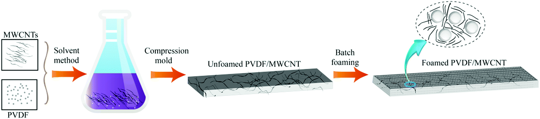
In this study, a facile two-step approach, which consisted of the preparation of solid PVDF/MWCNT nanocomposites and batch foaming, was used to fabricate the PVDF/MWCNT nanocomposite foams, as is shown in Fig. 1. First, the solid PVDF/MWCNT nanocomposites were fabricated. A solution-blending and compression-molding process was used to prepare the PVDF/MWCNT nanocomposites, which was similar to what was done in previous research.60,61 For a typical process, certain amounts of PVDF particles (5.0 g) were dissolved in 30 mL of DMF at 70 °C using a magnetic stirrer for 1 h, while an appropriate amount of MWCNTs (0.5 wt%) was simultaneously dispersed in DMF by sonication for 1 h. Subsequently, we added a MWCNT–DMF suspension to the PVDF-solution, and continued the stirring for 1 h. Then, the mixture was placed in a drying oven at 60 °C until the viscous liquid had completely evaporated. The obtained mixtures were compression molded in a designed mold at a temperature of 200 °C and a pressure of 30 MPa for 20 min. During the process, the nanocomposites were forced to deform in one direction, and eventually formed the “brick and mud” structure.
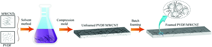 |
| | Fig. 1 Schematic of the fabrication procedures of lightweight PVDF/MWCNT nanocomposite foams. | |
2.3. Fabrication of lightweight PVDF/MWCNT nanocomposite foams
PVDF/MWCNT nanocomposite foams were prepared by a batch foaming process with supercritical CO2,62 and Fig. S1 (ESI†) shows the home-made batch foaming device used. In a typical experiment, the PVDF/MWCNT nanocomposites were cut into 15 mm × 15 mm × 10 mm sized pieces to be placed into a brass vessel. Next, CO2 was pressurized into the vessel using a syringe with a high-pressure liquid pump to achieve a supercritical CO2 state. When the required pressure was achieved, the system was kept at a given pressure (2000 psi) and at the designated temperature shown in Table 1 for 1 h to ensure that a sufficient amount of CO2 had dissolved into the PVDF matrix. After the soaking time, a rapid depressurization (1–2 s) was applied. The vessel was then immediately placed in a water/ice bath to stabilize the foams. We also investigated the influence of saturation temperature (167.5–170.5 °C) on both the foaming degree and the cellular morphology. For convenience, correspondingly, the PVDF/MWCNT nanocomposite foams were described as FC1–FC7 samples, as shown in Table 1.
Table 1 Processing parameters and void fraction of PVDF/MWCNT foams
| Foam sample |
FC1 |
FC2 |
FC3 |
FC4 |
FC5 |
FC6 |
FC7 |
| Temperature (°C) |
167.5 |
168 |
168.5 |
169 |
169.5 |
170 |
170.5 |
| Void fraction (%) |
45.7 |
55.7 |
69.5 |
84.3 |
65.6 |
50.4 |
48.7 |
2.4. Characterization
Cellular morphologies were analysed using a JEOL JSM 6060 scanning electron microscope (SEM). To take the pictures, the foamed samples were dried under vacuum conditions at 50 °C for 24 h and were freeze-fractured in liquid nitrogen. The fractured surface was sputter-coated with gold in an argon atmosphere. The X-ray radiation diffraction (XRD) spectra were used to identify the crystal phases, which were obtained using a Rigaku Smart Lab diffractometer (Tokyo, Japan) using Cu Kα radiation (λ = 0.15418 nm). The characteristic vibrational modes were analyzed using Fourier transform infrared spectroscopy (FTIR), which was carried out using a Nicolet iS10 FTIR spectrometer (USA). Raman spectra were collected using a LabRAM XploRA laser confocal Raman spectroscope (HORIBA Jobin Yvon Co., Ltd, Tokyo, Japan) with a 532 nm laser.
The void fraction (Vf) of the foamed samples was estimated as Vf = 1 − ρf/ρ, where ρf and ρ were the foamed and solid sample densities, respectively. The sample densities before (ρ) and after foaming (ρf) were determined via the water displacement method according to ASTM D 2325. Image analysis to evaluate the mean cell size was manually performed and was based on the SEM pictures. This was done by measuring the size of at least 100 cells. The electrical conductivities of the foam samples were obtained using a four-probe method using a Keithley 4200 electrometer (Keithley, USA).
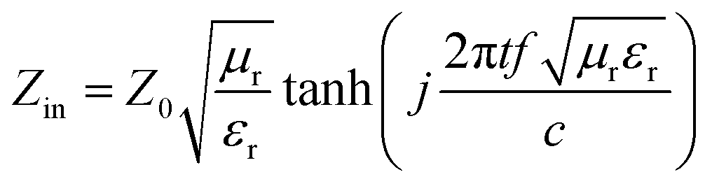
The PVDF/MWCNT nanocomposite foams were cut into shapes with dimensions of 10.65 mm × 4.31 mm × 2.5 mm to measure the relative complex permittivity εr (εr = ε′ − jε′′) and permeability μr (μr = μ′ − jμ′′) using the waveguide method in the K-band (18–26.5 GHz). Based on the metal backplane model, the sample's RL was determined from the measured complex permeability and permittivity, according to the following equations:25,35,63,64
| | | RL = 20log10|(Zin − Z0)/(Zin + Z0)| | (1) |
| |  | (2) |
where
Z0 = 377 Ω is the impedance of air, and
Zin is the input impedance of the absorbers; additionally,
f is the frequency,
c is the velocity of light, and
t is the absorber thickness, respectively. When the RL is smaller than −10 dB, only 10% of the microwave energy is reflected, while 90% is absorbed. The corresponding frequency range, over which the RL is smaller than −10 dB, is defined as the effective absorption bandwidth.
3. Results and discussion
3.1. Characterization of PVDF/MWCNT nanocomposite foams
The raw MWCNTs and the PVDF/MWCNT nanocomposites were characterized using transmission electron microscopy (TEM), and the results are shown in Fig. S2 (ESI†). Due to inter-molecular forces, the isolated MWCNTs of different sizes and directions formed an aggregated structure. The TEM image (Fig. S2a, ESI†) shows that the MWCNTs had a length of several micrometers and an outer diameter of 5–15 nm. Fig. S2b (ESI†) shows the quality of the MWCNT dispersion in the PVDF before foaming. The TEM micrograph shows that a homogenous dispersion of MWCNTs in the PVDF matrix was achieved by simply mechanically mixing the MWCNTs with PVDF in a PVDF solution.
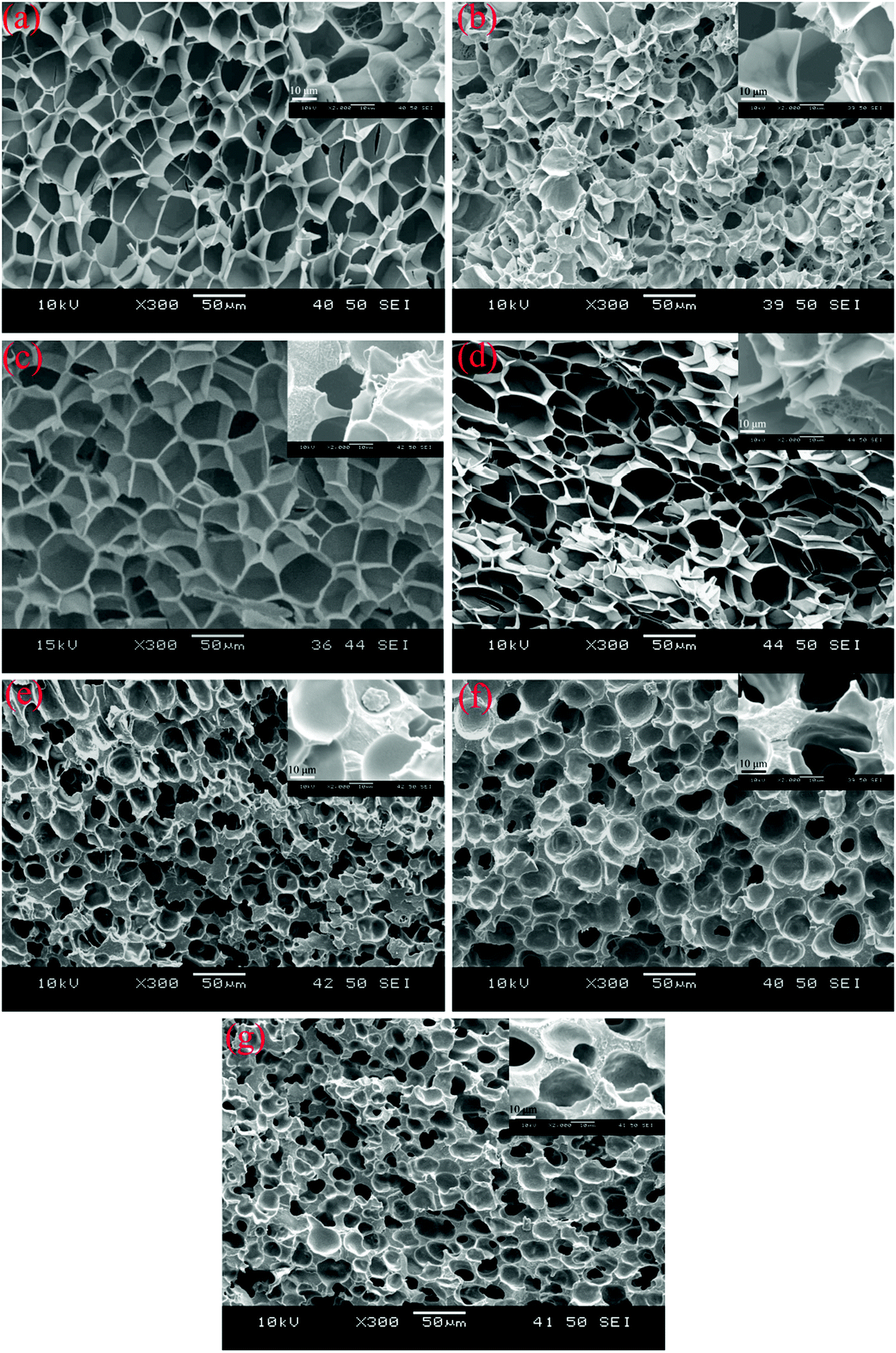
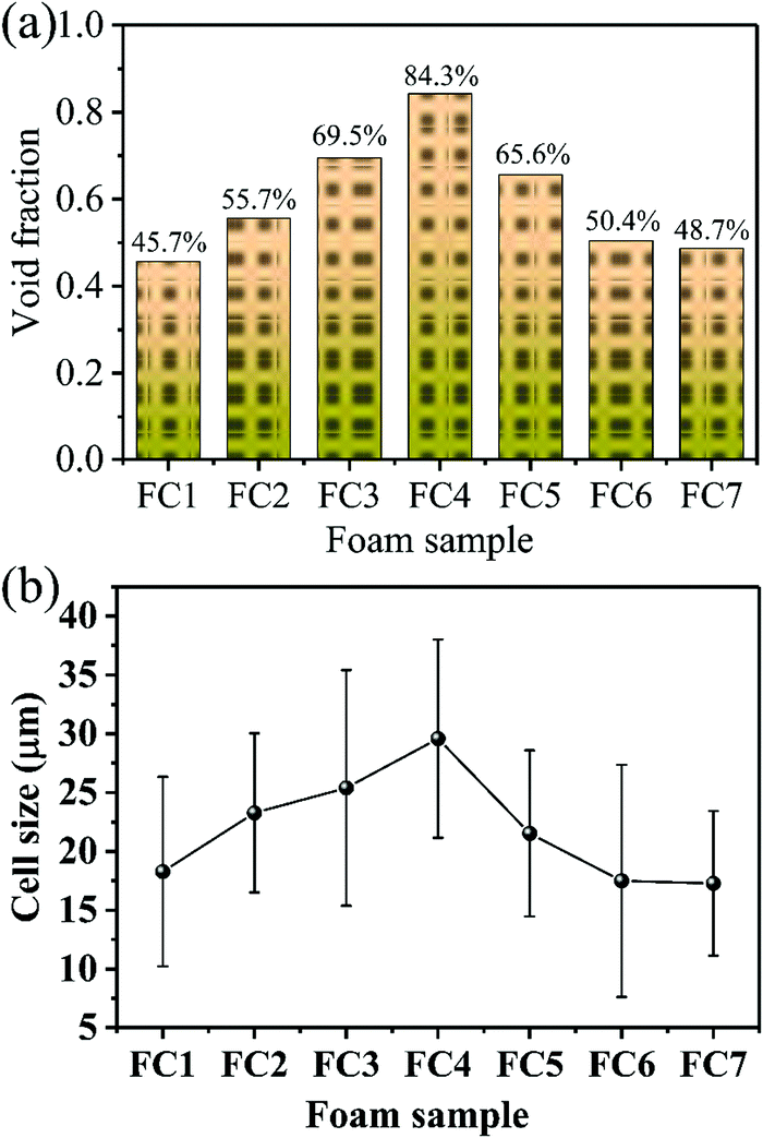
To identify the crystal structure of PVDF in the matrix of the foamed nanocomposites, XRD analysis was done, and Fig. S3 (ESI†) shows the spectra. The diffraction spectra of all the PVDF/MWCNT nanocomposite foams displayed peaks at 2θ = 17.5° (100), 18.2° (020), 19.8° (021), and 26.6° (201), which were assigned to the nonpolar α phase.65,66 In addition, it is noteworthy that the PVDF/MWCNT composite foams prepared for this study showed a broad peak at around 2θ = 20.6°, which was indicative of a polar β-crystalline phase (200) and (110) peaks.67 The XRD results in these foams indicated the presence of a semi-crystalline mixture of α- and β-phases of the PVDF polymer. The PVDF β-phases were expected to play a positive role in enhancing the microwave absorption properties.39,68 To further confirm the α- and β-phases in the PVDF/MWCNT composite foams, their FTIR spectra were studied, and Fig. 2 shows the results. FTIR is one of the finest measurement techniques used to identify the different PVDF polymorphs. The FTIR spectrum of the PVDF/MWCNT foams showed absorption bands at 767 cm−1 (CF2 skeletal bending), and 796 and 976 cm−1 (CH2 rocking), which were attributed to the nonpolar α-phase.67 The absorption bands at 840, 872, and 1175 cm−1 were attributed to the β-phase. The bands at 840 cm−1 and 872 cm−1 were assigned to the CH2 and CF2 groups, which were generated from the CH2 rocking, CF2 stretching, and skeletal C–C stretching.69 The band at 1175 cm−1 was assigned to the CH2 group, which was associated with the CH2 wagging and rocking mechanism.53 The CH2's in-plane bending or scissoring was observed at 1402 cm−1, while the C–C–C-bending appeared at 1070 cm−1.70 Thus, by combining the XRD and FTIR results, we concluded that the α- and β-phases of PVDF co-existed in the PVDF/MWCNT nanocomposite foams. More detailed structural information on the carbon materials was further obtained from the Raman spectra. In Fig. S4 (ESI†), the Raman spectra of the PVDF/MWCNT nanocomposite foams show two distinct peaks; namely, one at ∼1350 cm−1, called the D band and the other at ∼1590 cm−1, called the G band. The former stemmed from the presence of defects and disorder, while the latter was ascribed to the vibration of the sp2 carbon atoms.71,72 The intensity ratio of the D-band to the G-band (ID/IG) is usually employed to determine the graphitic materials’ defects. In general, a higher ID/IG ratio indicates a high graphitic disorder in the carbon.73 In Fig. S4 (ESI†), the PVDF/MWCNT nanocomposite foams displayed higher ID/IG values with a higher foaming degree (void fraction). This indicates that foaming could increase the MWCNT's disorder. Thus, it affected the electrical conductivity and the MA properties, which are discussed in the following paragraphs. MWCNTs were reported to provide nucleating sites in the heterogeneous cell-nucleating process.39,53 In the heterogeneous nucleating process, cell nucleation took place in the boundary between the polymer matrix and the dispersed filler particles, and the activation energy barrier to nucleation was reduced.74,75Fig. 3 shows the morphological observation of the PVDF/MWCNT nanocomposite foams prepared at different saturation temperatures. The foams’ cellular morphology presented a uniform foaming behavior, which was attributed to the increased melt strength and the slowing down of gas loss by the “brick and mud” structure. Moreover, the nanocomposite foams’ morphology showed clear changes in the cellular shape, size, and wall thickness. In the highly magnified SEM images (insets in Fig. 3), the MWCNTs were observed in the cell walls. Fig. 4 shows the void fraction and the average cell size of the PVDF/MWCNT nanocomposite foams. In agreement with this, the foaming degree (the void fraction) (Fig. 4a) first increased and then decreased with increased saturation temperature. Notably, the average cell size first increased and then decreased with an elevated saturation temperature (Fig. 4b). Thus, it can be concluded that the cell parameters (density, void fraction, and cell size) could be validly determined by the foaming temperature. Therefore, this phenomenon offers a possible route towards the relationship between the electrical conductivity, the microwave absorption, and the microcellular structure in designable PVDF/MWCNT foams. Taking FC2 as an example, the microstructure of the PVDF/MWCNT foam was further characterized by high-magnification SEM and TEM, and the results are shown in Fig. S5 (ESI†). One can notice that the MWCNTs were oriented along the cell walls of the PVDF polymer because of their biaxial stretching from cell growth.
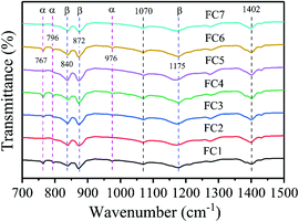 |
| | Fig. 2 FT-IR spectra of various PVDF/MWCNT nanocomposite foams. | |
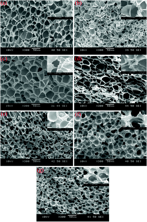 |
| | Fig. 3 SEM images of various PVDF/CNT nanocomposite foams: (a) FC1; (b) FC2; (c) FC3; (d) FC4; (e) FC5; (f) FC6; and (g) FC7. Insets are the corresponding high magnification SEM images. | |
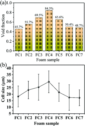 |
| | Fig. 4 (a) The void fraction, and (b) the cell size of various PVDF/CNT nanocomposite foams fabricated at different saturation temperatures. | |
3.2. Electrical conductivity of the PVDF/MWCNT nanocomposite foams
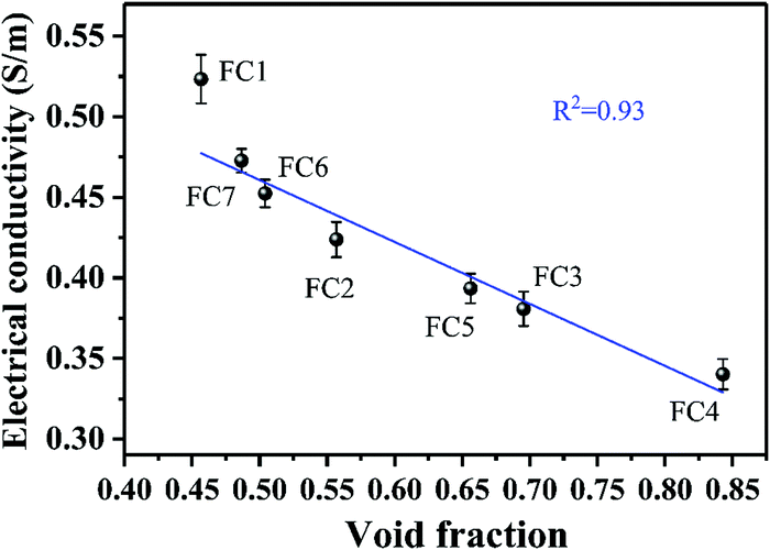
To investigate how the foaming degree (void fraction) influenced the electrical conductivity of the PVDF/MWCNT nanocomposite foams, we plotted the electrical conductivity as a function of the void fraction, and the results are shown in Fig. 5. Based on the overview, the electrical conductivity declined linearly with the elevated void fraction. Compared with the unfoamed PVDF/MWCNT nanocomposite's counterpart (0.44 S m−1), it was interesting to find that the PVDF/MWCNT nanocomposite foams with a void fraction of below 50% had a higher electrical conductivity. Otherwise, when the void fraction of the nanocomposite foams was above 50%, the foams’ electrical conductivity was less than that of the unfoamed PVDF/MWCNT nanocomposite. In other words, the microcellular structure played a positive role in boosting the electrical conductivity when the nanocomposite foams’ void fraction was lower than 50%. Otherwise, the cellular structure would have played a negative role in the electrical conductivity. On the basis of Ameli's theory,54 in the PP/MWCNT nanocomposite foams, when foaming began, the biaxial stretching caused the MWCNTs to slightly orient around the cells, and cell-to-cell compression made the MWCNTs connect to enhance their interconnections. Thus, this action increased the electrical conductivity. However, when the degree of foaming was increased beyond an optimum point, the MWCNTs became fully oriented and normal to the radial direction (similar to planar orientation). Consequently, the conductivity started to decrease. In the PVDF/MWCNT nanocomposite foam, the variation of the electric conductivity was determined by the foaming degree.
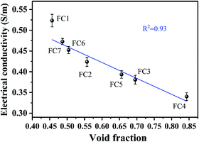 |
| | Fig. 5 The relationship between the electrical conductivity and the foaming degree (void fraction) for various PVDF/MWCNT nanocomposite foams. | |
3.3. MA properties of the PVDF/MWCNT nanocomposite foams
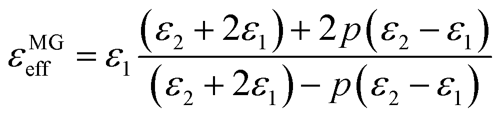
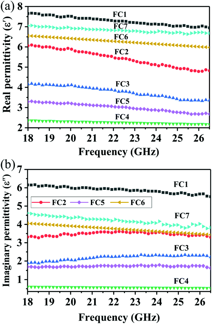
As is well known, the absorption properties of EM absorbers are closely related to the absorber's EM parameters; that is, their complex permittivity (εr = ε′ − jε′′) and permeability (μr = μ′ − jμ′′). The real parts of the complex permittivity (ε′) and the complex permeability (μ′) symbolize the storage capabilities of the electric and magnetic energies, respectively. In addition, the imaginary parts, (ε′′) and (μ′′), are associated with the EM energy's dissipation energies, respectively.76,77 In addition, the EM wave absorption properties also depend on the dissipation capability as well as on proper impedance matching.20,78Fig. 6 shows the frequency dependence of the real and imaginary parts of the PVDF/MWCNT nanocomposite foams’ permittivity. Due to the presence of the non-magnetic constituent (μr ∼ 1), we mainly focus on the relative complex permittivity. As shown in Fig. 6a, the real part (ε′) of the PVDF/MWCNT nanocomposite foams’ complex permittivity declined with an increase in void fraction, and the FC1 foam, with a void fraction of 45.7%, showed the highest real (ε′) values. It is also well known that a porous material is composed of a solid and a void. Therefore, a porous material can be treated as an “effective medium,” whose effective permittivity (which is defined in ref. 70 and 79) can be obtained by using the Maxwell Garnett equation as follows:25,79,80| | 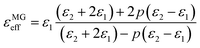 | (3) |
where ε1 and ε2 are the permittivity of the solid state and gas state, respectively, and p stands for the void's volume fraction in the effective medium. Consequently, porous structures can decrease their effective permittivity, according to the Maxwell Garnett theory. In our study, the real parts (ε′) of the PVDF/MWCNT nanocomposite foams could be effectively monitored by the foaming degree (void fraction). A higher void fraction caused a lower ε′ value, and the variation tendency of the ε′ values completely agreed with the Maxwell Garnett theory. The void in foams could lead to a small real permittivity,54 which would improve the impedance match to make it more possible for the microwaves to enter the absorber.81
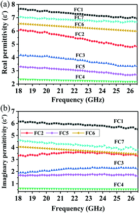 |
| | Fig. 6 (a) The real part (ε′) and (b) imaginary part (ε′′) of the permittivity as a function of the frequency for various PVDF/MWCNT nanocomposite foams. | |
For the imaginary permittivity (ε′′) and the dielectric dissipation tangent (tanδε = ε′′/ε′), similarly, the FC1 foam with the highest electrical conductivity at the smallest void fraction, and the FC4 foam with the lowest electrical conductivity at the largest void fraction, presented the highest and the lowest ε′′ and tanδε values (Fig. 6b and Fig. S6, ESI†), respectively. According to the free electron theory,82ε′′ ≈ σ/(2πε0f), where σ is the electrical conductivity, and a high electrical conductivity indicates a high ε′′ and dielectric loss values. This equation demonstrates the strong link between the conductivity and the ε′′ value. Fig. 5 shows how the electrical conductivity of the PVDF/MWCNT foams decreased with an increased void fraction. Correspondingly, similar changes in the ε′′ and the dielectric loss curves were obtained, and the FC1 foam possessed the highest ε′′ and dielectric loss values of the seven foam samples, which may have given it excellent MA properties. It is generally known that the dielectric loss originates mainly from the conductive and polarization losses, which include ionic polarization, electronic polarization, dipole orientation polarization, and interfacial polarization.83 Given that the electron polarization and ion polarization usually are generated at the THz and PHz scales, for microwave GHz frequencies, the dipole orientation polarization and the interfacial polarization contribute the most to MA. The conduction loss depends on the composites’ electrical conductivity, which can be determined from their corresponding carbon materials.
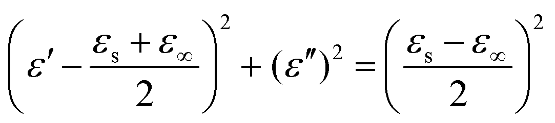
The heterogeneous interfaces between the MWCNTs, air, and the PVDF induce space charge accumulations at the interface,84 and these lead to interfacial polarization. In addition, two PVDF phases existed in the composite foams, and uneven charge accumulation took place under an electric field. This action favored microwave dissipation, which was similar to what other researchers have reported on dual-phase TiO285 and dual-phase Co.86 The Debye theory is a powerful tool to understand the PVDF/MWCNT foams’ polarization mechanism. According to this theory,87ε′ and ε′′ can be expressed as follows:
| | 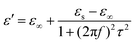 | (4) |
| |  | (5) |
Herein,
εs,
τ, and
ε∞ are the static permittivity, polarization relaxation time, and the relative dielectric permittivity at the high-frequency limit, respectively. By subtracting the contribution of the
σ from the
ε′′, and by eliminating the 2π
fτ, the relationship between
ε′ and
ε′′ should be a semi-circle; namely,

, which is generally denoted as the Cole–Cole semi-circle.
88 Each semi-circle corresponds to a single Debye relaxation process. As shown in Fig. S7 (ESI
†), the FC2, FC3, and FC5 foams had multiple Cole–Cole semi-circles that represent different Debye relaxation behaviors. Such behaviors may be closely related to the interface polarization between the PVDF, air, and the MWCNTs. Under alternating EM radiation, the lags of induced charges originating from the PVDF–MWCNTs, PVDF–air, MWCNTs–MWCNTs, and PVDF–PVDF interfaces, which meet the externally applied field, lead to the relaxation process and transform the EM energy into thermal energy.
89 It is noteworthy that the Cole–Cole semi-circles were distorted, indicating that the as-prepared composite foams were not ideal models for the Debye equation, and that some other mechanisms, like the Maxwell–Wagner relaxation, exist.
11 We further note that when the dielectric loss was increased by elevating the electrical conductivity, the conduction loss also played a major part in enhancing the attenuation of microwaves.
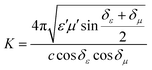
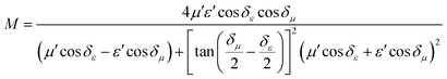
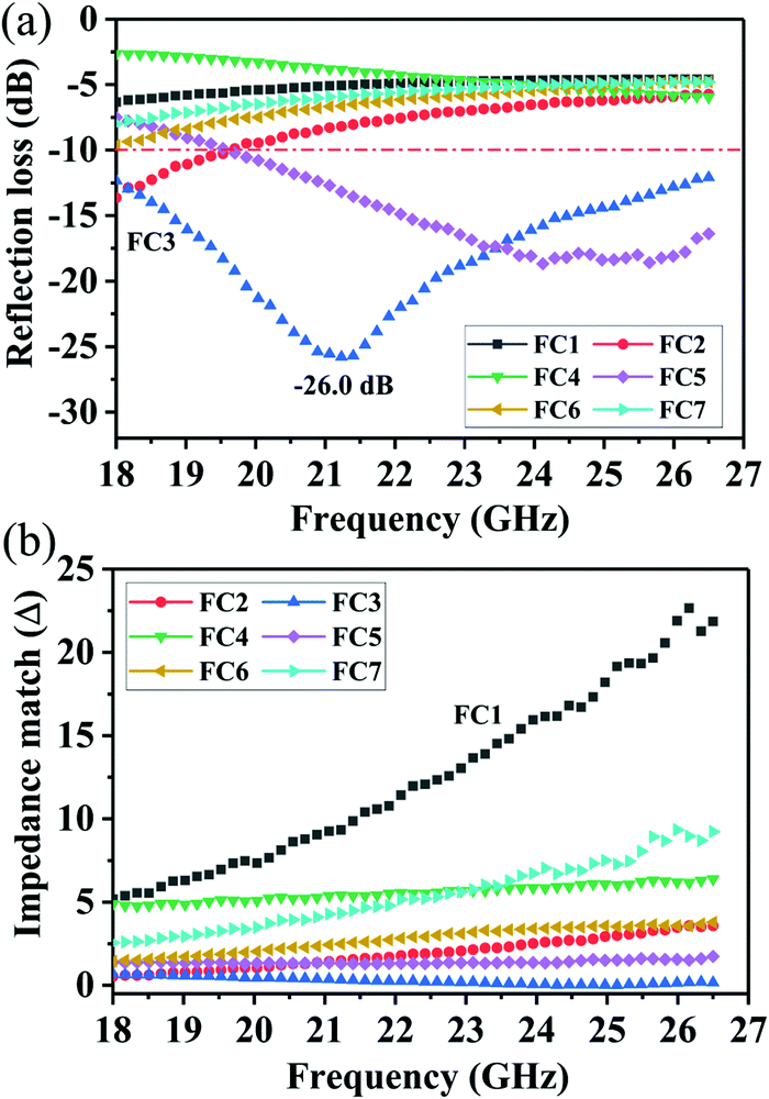
To further evaluate the EM wave absorption properties, the RL values of the PVDF/MWCNT nanocomposite foams were calculated at a given absorber thickness of 2.0 mm in the frequency range of 18–26.5 GHz. The RL value, which was below −10 dB, indicated that up to 90% of the EM energy had been absorbed and only 10% of it had been reflected.11Fig. 7a shows the RL values of various PVDF/MWCNT nanocomposite foams. In comparison with the unfoamed PVDF/MWCNT nanocomposite sample (shown in Fig. S8, ESI†), all the foamed PVDF/MWCNT nanocomposite samples displayed enhanced MA properties, which indicated that the introduction of a microcellular structure could boost the PVDF/MWCNT nanocomposite's performance. Remarkably, the FC3 foam exhibited outstanding MA. The optimal reflection loss was −26 dB, and the effective bandwidth of the RL values below −10 dB covered the entire measured frequency (Fig. 7a). Furthermore, the microwave absorption properties of nanocomposite foams at a frequency of 2–18 GHz were also investigated, and the results are shown in Fig. S9 (ESI†). Notably, it is clearly seen that the microwave band (2–18 GHz) of these samples has a relatively strong absorbing ability, which could also be used in the low frequency (2–18 GHz). Additionally, the pure PVDF foam has almost no electromagnetic wave absorption capability (Fig. S10, ESI†). In our previous discussion, owing to the highest dielectric loss of the FC1 foam, the FC1 foam showed the highest MA. However, herein, the FC3 foam sample exhibited the best MA properties. To design a high-efficiency MA material, two key factors, namely, strong dissipation capability and impedance match, should be considered.11 To understand why the FC3 foam exhibited the strongest MA properties, we should consider another important factor of impedance matching (which allowed microwaves to pass through the absorbers).90 To obtain zero reflection on the samples’ front surfaces, their characteristic impedance should be equal or close to that of the free space. To achieve good impedance matching, it is necessary for the material to have the same or similar εr and μr. The impedance matching degree Δ, which was proposed by Ma's team,91 can be expressed by the following equations:36,92
| | | |Δ| = |sinh2(Kfd) − M| | (6) |
and the values of
K and
M are also calculated through the complex permittivity and permeability by the following equations:
| |  | (7) |
| |  | (8) |
It is noteworthy that a smaller absolute value of delta (
Δ) means there is a better impedance matching.
Fig. 7b displays the absolute delta value maps for various PVDF/MWCNT nanocomposite foams in the frequency range of 18–26.5 GHz, with a thickness of 2.0 mm. It is clear that the FC3 had the smallest delta (
Δ) value. This indicates that the FC3 foam sample should have superior impedance matching ability and also show better MA performance.
 |
| | Fig. 7 (a) Reflection loss and (b) impedance match (Δ) of PVDF/MWCNT nanocomposite foams with a thickness of 2.0 mm. | |
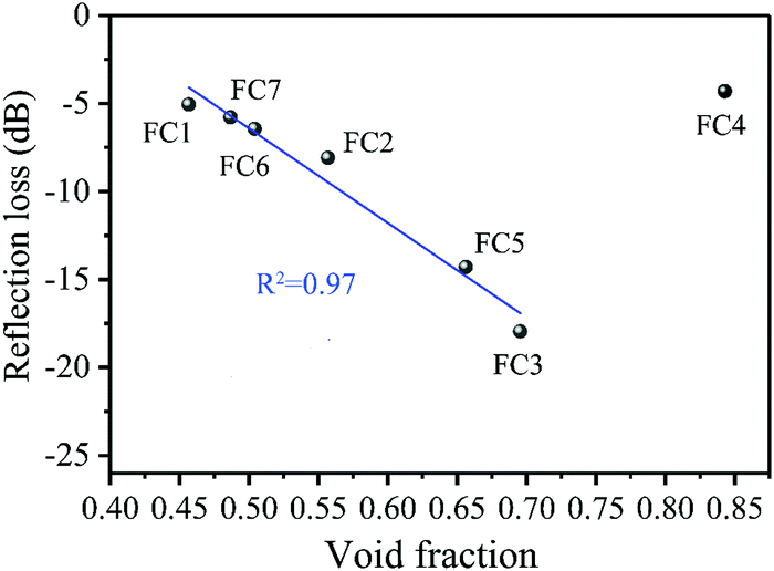
The above results indicate that a microcellular structure effectively tuned the complex permittivity and further improved the impedance match. This would benefit the MA properties. To directly show the correlation between the MA properties and the cellular structure, we plotted the average RL values as a function of the foaming degree (void fraction). The results are shown in Fig. 8. The RL values decreased linearly with an increased void fraction. This means that the MA properties were enhanced linearly by elevating the void fraction when it was below the critical value of 75%. It is also significant that when the void fraction was above 75%, the RL values increased and the MA decreased. Understandably, the high void fraction would induce a low electrical conductivity and dielectric loss, and thus lead to weak MA. In this study, by controlling the void fraction, we were able to obtain high-efficiency MA properties. The result was a novel way to design suitable lightweight absorbers with a wide-band and strong absorption.
 |
| | Fig. 8 The correlation between the average RL value and the foaming degree (void fraction) for various PVDF/MWCNT nanocomposite foams. | |
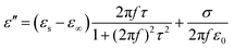
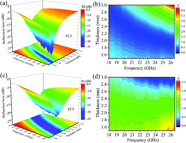
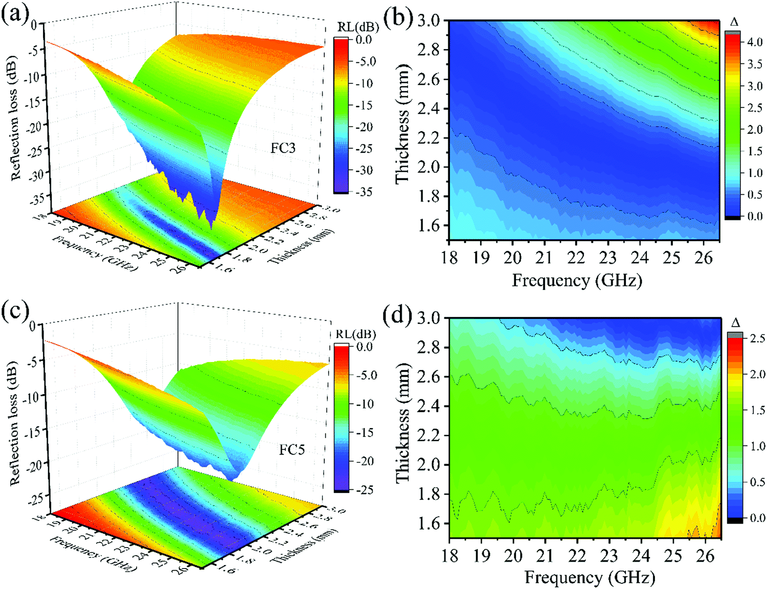
According to eqn (1) and (2), the EM wave absorption properties were also closely associated with the absorber's thickness. Fig. 7a shows that the FC3 and FC5 foams had high MA properties. To show how the absorber thickness influenced the MA properties, the 3-D image maps of the RL values and the delta (Δ) value maps of the FC3 and FC5 foams with various absorber thicknesses (1.5–3.0 mm) are shown in Fig. 9. As shown in Fig. 9(a and c), the effective bandwidth (8.5 GHz in the whole frequency) was obtained in most of the measured absorber thicknesses. The minimal RL of −34.1 dB (99.9% microwave dissipation) can be seen in the FC3 foam with a thickness of 1.7 mm (Fig. 9a), and the optimal RL of −19.2 dB can be observed in the FC5 foam with a thickness of 1.95 mm. Fig. 9b and d display the calculated delta value maps of the FC3 and FC5 foam samples with absorber thicknesses of 1.5–3.0 mm. The results clearly indicate that the FC3 foam sample had a larger area below 0.5 than the FC5 foam sample. This finding is consistent with the above analysis of the MA properties, and it suggests that the FC3 foam sample's MA performance was superior. To show the superior properties of the PVDF/MWCNT nanocomposites, the results of this work were compared with other microwave absorbers and are shown in Table 2. One can see that the PVDF/MWCNT foams exhibit the advantages of strong absorption, wide bandwidth and ultra-low content filler (Table 2).
 |
| | Fig. 9 (a) Three dimensional RL values and (b) calculated delta value map of the FC3 foam sample; (c) three dimensional RL values and (d) calculated delta value map of the FC5 foam sample. | |
Table 2 MA performance of some microwave absorbing materials
| Materials |
RLmin (dB) |
Thickness (mm) |
Bandwidth (RL ≤ −10 dB) |
Filler content (wt%) |
Matrix |
Ref. |
| CoS2/N doped CNTs |
−65 |
1.6 |
6.2 (13.8–18) |
50 |
Paraffin |
4
|
| CuS/NiFe2O4/graphene |
−54.5 |
2.5 |
4.5 (9.7–14.2) |
20 |
Paraffin |
5
|
| Nickel/carbon |
−17.8 |
1.5 |
4.8 (13.2–18) |
30 |
Paraffin |
8
|
| Co/C crabapples |
−26.6 |
2.0 |
5.8 (12.2–18.0) |
30 |
Paraffin |
9
|
| Core–shell Co@C |
−68.7 |
1.65 |
4.2 (8.6–12.8) |
70 |
Paraffin |
11
|
| Edge-rich graphene |
−26.7 |
3.75 |
4.2 (8.2–12.4) |
— |
Si3N4 |
12
|
| FeCo/porous carbon |
−21.7 |
1.2 |
5.8 (12.2–18.0) |
50 |
Paraffin |
20
|
| Graphene@PANI@TiO2 |
−45.4 |
1.5 |
4.4 (12.3–16.7) |
50 |
Paraffin |
22
|
| Nano-porous carbon |
−42.4 |
2.0 |
1.76 (8.08–9.84) |
70 |
Paraffin |
25
|
| Mesoporous hollow carbon |
−84 |
3.9 |
4.8 (6.8–11.6) |
20 |
Paraffin |
28
|
| ZnO nanowires/reduced graphene foams |
−27.8 |
4.8 |
4.2 (8.2–12.4) |
3.3 |
Poly(dimethylsiloxan) |
31
|
| SiC nanowires/lamellar carbon foams |
−31 |
3.3 |
4.2 (8.2–12.4) |
0.8 |
Epoxy |
32
|
| Graphene aerogel/carbon fiber |
−30.53 |
1.5 |
4.1 (12.7–16.8) |
20 |
Paraffin |
33
|
| Graphene/SiC Nanowire Foam |
−19.6 |
3 |
4.2 (8.2–12.4) |
— |
Poly(dimethylsiloxan) |
35
|
| MWCNT/PVDF foams |
−31 |
1.85 |
7.8 (18.7–26.5) |
0.5 |
PVDF |
This work |
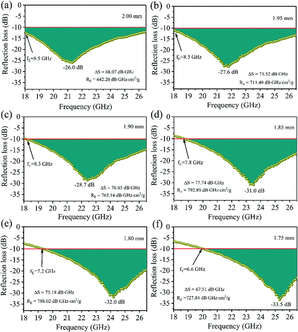 |
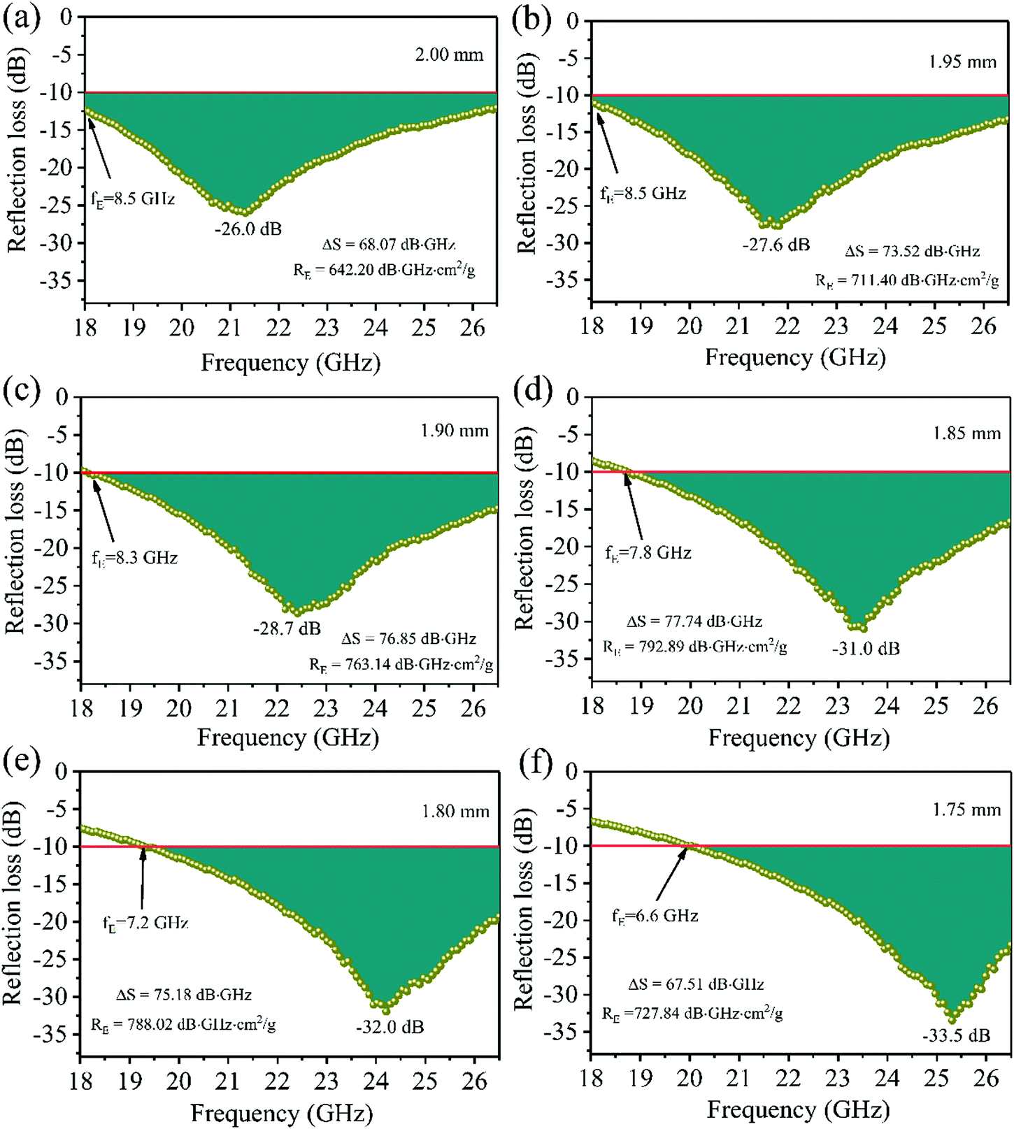
| | Fig. 10 Reflection loss values of the FC3 foam sample with certain thicknesses: (a) 2.00, (b) 1.95, (c) 1.90, (d) 1.85, (e) 1.80, and (f) 1.75 mm. | |
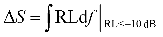
Until now, it has been difficult to evaluate the MA performance of the absorbers because of the many factors that must be taken into consideration. These include the minimal RL peak, the bandwidth, the density, and the absorber thickness. Thus, based on Zhang's theory,34 a novel strategy integrated with significant MA indicators such as thickness, density, qualified bandwidth and RL values was used to verify the EM wave absorption properties of the absorber. At first, we defined ΔS, which is equal to the shaded area when the RL is below −10 dB. It can be expressed as follows:93 . When the absorber thicknesses were 2.00 mm, 1.95 mm, 1.90 mm, 1.85 mm, 1.80 mm and 1.75 mm, the corresponding ΔS values were 68.07, 73.52, 76.85, 77.74, 75.18 and 67.51 dB GHz (Fig. 10), respectively. Second, the EM absorption efficiency RE is defined as ΔS/td (t is the thickness and d is the density); namely, RE = ΔS/td. The RE values of the six absorber thicknesses were 642.20, 711.40, 763.14, 792.89, 788.02, and 727.84 dB GHz cm2 g−1, respectively. Thus, it could be deduced that when the absorber thickness of the FC3 foam was 1.85 mm, the best MA properties were obtained (RLmin = −31.0 dB, bandwidth of 7.8 GHz, ΔS = 77.74 dB GHz, and RE = 792.89 dB GHz cm2 g−1).
The excellent MA of the PVDF/MWCNT nanocomposite foams with a void fraction of 69.5% was due to several factors. One is the possible MA mechanism, which is shown in Fig. 11. First, due to the presence of numerous cells and a large solid–air interface area, the complex permittivity could be effectively tuned and, consequently, the degree of impedance matching could be largely improved. Therefore, more EM waves can enter the absorbers and dissipate via the following mechanisms. Second, the EM wave undergoes multiple reflections and scattering inside the interior voids,38,94 which prolongs the propagation path in the samples, causing it to become further attenuated, and the ratio of absorption/reflection increases. Third, the existence of more interfaces between the PVDF, the air bubbles, and the MWCNTs leads to the accumulation of charges at the interfaces, and these interfaces result in interfacial polarization.95 Fourth, due to the composite foams’ relatively high electrical conductivity, the conduction loss, which is associated with the attenuation of energy through the current flow via the migration, hopping, and tunneling mechanisms,96,97 contributes to the MA properties.
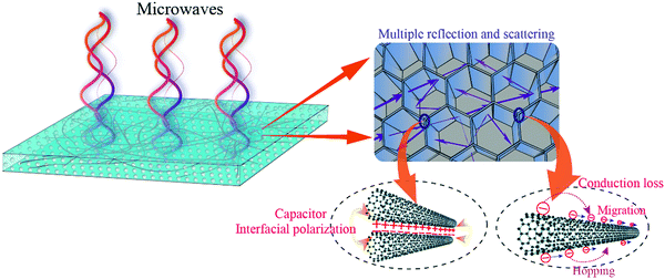 |
| | Fig. 11 Schematic of the possible EM wave absorption mechanism of the PVDF/MWCNT nanocomposite foams. | |
4. Conclusion
In summary, we used a home-made batch foaming method to fabricate novel PVDF/MWCNT nanocomposite foams. Nanocomposite foams with various void fractions were obtained by controlling the saturation temperature. The electrical conductivity, the dielectric permittivity, and the MA properties of PVDF/MWCNT nanocomposite foams were effectively tuned by adjusting the foaming degree (void fraction). The electrical conductivity was decreased linearly by increasing the void fraction in the range of 45.7–84.3%. The dielectric permittivity also decreased with an increased void fraction in the same range. The MA properties increased with the increased void fraction when it was below the critical value of 75%. The PVDF/MWCNT nanocomposite foam (FC3) with a void fraction of 69.5% displayed excellent MA properties. The optimal reflection loss was −26 dB with an absorber thickness of 2.0 mm, and an effective bandwidth of RL values below −10 dB covered the entire measured frequency (18–26.5 GHz). Moreover, we used a comprehensive strategy to evaluate MA, and the results showed that when the FC3 foam's absorber thickness was 1.85 mm, the best MA properties were obtained (RLmin = −31.0 dB, bandwidth of 7.8 GHz, ΔS = 77.74 dB GHz, and RE = 792.89 dB GHz cm2 g−1). This PVDF/MWCNT nanocomposite foam is therefore a promising microwave absorber offering superior properties of high-efficiency and wide-band absorption small thickness, and light weight.
Conflicts of interest
There are no conflicts to declare.
References
- J. Ru, Y. Fan, W. Zhou, Z. Zhou, T. Wang, R. Liu, J. Yang, X. Lu, J. Wang, C. Ji, L. Wang and W. Jiang, ACS Appl. Mater. Interfaces, 2018, 10, 39245–39256 CrossRef CAS.
- Q. Liu, Q. Cao, H. Bi, C. Liang, K. Yuan, W. She, Y. Yang and R. Che, Adv. Mater., 2016, 28, 486–490 CrossRef CAS.
- X. Li, X. Yin, C. Song, M. Han, H. Xu, W. Duan, L. Cheng and L. Zhang, Adv. Funct. Mater., 2018, 28, 1803938 CrossRef.
- J. Yan, Y. Huang, X. Han, X. Gao and P. Liu, Composites, Part B, 2019, 163, 67–76 CrossRef CAS.
- P. Liu, Y. Huang, J. Yan, Y. Yang and Y. Zhao, ACS Appl. Mater. Interfaces, 2016, 8, 5536–5546 CrossRef CAS.
- L. Lv, J. Liu, C. Liang, J. Gu, H. Liu, C. Liu, Y. Lu, K. Sun, R. Fan, N. Wang, N. Lu, Z. Guo and E. K. Wujcik, Eng. Sci., 2018, 2, 26–42 Search PubMed.
- C. Wang, V. Murugadoss, J. Kong, Z. He, X. Mai, Q. Shao, Y. Chen, L. Guo, C. Liu, S. Angaiah and Z. Guo, Carbon, 2018, 140, 696–733 CrossRef CAS.
- P. Xie, H. Li, B. He, F. Dang, J. Lin, R. Fan, C. Hou, H. Liu, J. Zhang, Y. Ma and Z. Guo, J. Mater. Chem. C, 2018, 6, 8812–8822 RSC.
- N. Wu, C. Liu, D. Xu, J. Liu, W. Liu, H. Liu, J. Zhang, W. Xie and Z. Guo, J. Mater. Chem. C, 2019, 7, 1659–1669 RSC.
- N. Li, Y. Huang, F. Du, X. He, X. Lin, H. Gao, Y. Ma, F. Li, Y. Chen and P. C. Eklund, Nano Lett., 2006, 6, 1141–1145 CrossRef CAS.
- D. Ding, Y. Wang, X. Li, R. Qiang, P. Xu, W. Chu, X. Han and Y. Du, Carbon, 2017, 111, 722–732 CrossRef CAS.
- F. Ye, Q. Song, Z. Zhang, W. Li, S. Zhang, X. Yin, Y. Zhou, H. Tao, Y. Liu, L. Cheng, L. Zhang and H. Li, Adv. Funct. Mater., 2018, 28, 1707205 CrossRef.
- Y.-J. Wan, P.-L. Zhu, S.-H. Yu, R. Sun, C.-P. Wong and W.-H. Liao, Small, 2018, 14, 1800534 CrossRef.
- Y.-J. Wan, P.-L. Zhu, S.-H. Yu, R. Sun, C.-P. Wong and W.-H. Liao, Carbon, 2017, 115, 629–639 CrossRef CAS.
- Y.-J. Wan, P.-L. Zhu, S.-H. Yu, R. Sun, C.-P. Wong and W.-H. Liao, Carbon, 2017, 122, 74–81 CrossRef CAS.
- J. Guo, H. Song, H. Liu, C. Luo, Y. Ren, T. Ding, M. A. Khan, D. P. Young, X. Liu, X. Zhang, J. Kong and Z. Guo, J. Mater. Chem. C, 2017, 5, 5334–5344 RSC.
- L. Wang, H. Qiu, C. Liang, P. Song, Y. Han, Y. Han, J. Gu, J. Kong, D. Pan and Z. Guo, Carbon, 2019, 141, 506–514 CrossRef CAS.
- B. Zhao, C. Zhao, M. Hamidinejad, C. Wang, R. Li, S. Wang, K. Yasamin and C. B. Park, J. Mater. Chem. C, 2018, 6, 10292–10300 RSC.
- G. Sun, B. Dong, M. Cao, B. Wei and C. Hu, Chem. Mater., 2011, 23, 1587–1593 CrossRef CAS.
- X. Zhang, G. Ji, W. Liu, B. Quan, X. Liang, C. Shang, Y. Cheng and Y. Du, Nanoscale, 2015, 7, 12932–12942 RSC.
- Y. Chen, H.-B. Zhang, Y. Yang, M. Wang, A. Cao and Z.-Z. Yu, Adv. Funct. Mater., 2015, 26, 447–455 CrossRef.
- P. Liu, Y. Huang, J. Yan and Y. Zhao, J. Mater. Chem. C, 2016, 4, 6362–6370 RSC.
- H. Wu, X. Huang and L. Qian, Eng. Sci., 2018, 2, 17–25 Search PubMed.
- Z. Wang, R. Wei, J. Gu, H. Liu, C. Liu, C. Luo, J. Kong, Q. Shao, N. Wang, Z. Guo and X. Liu, Carbon, 2018, 139, 1126–1135 CrossRef CAS.
- X. Qiu, L. Wang, H. Zhu, Y. Guan and Q. Zhang, Nanoscale, 2017, 9, 7408–7418 RSC.
- T. Liu, Y. Pang, M. Zhu and S. Kobayashi, Nanoscale, 2014, 6, 2447–2454 RSC.
- M. Yu, C. Liang, M. Liu, X. Liu, K. Yuan, H. Cao and R. Che, J. Mater. Chem. C, 2014, 2, 7275–7283 RSC.
- H. Xu, X. Yin, M. Zhu, M. Han, Z. Hou, X. Li, L. Zhang and L. Cheng, ACS Appl. Mater. Interfaces, 2017, 9, 6332–6341 CrossRef CAS.
- C.-H. Cui, D.-X. Yan, H. Pang, L.-C. Jia, X. Xu, S. Yang, J.-Z. Xu and Z.-M. Li, Chem. Eng. J., 2017, 323, 29–36 CrossRef CAS.
- Z. Zeng, H. Jin, M. Chen, W. Li, L. Zhou, X. Xue and Z. Zhang, Small, 2017, 13, 1701388 CrossRef.
- C. Song, X. Yin, M. Han, X. Li, Z. Hou, L. Zhang and L. Cheng, Carbon, 2017, 116, 50–58 CrossRef CAS.
- S. Xiao, H. Mei, D. Han, K. G. Dassios and L. Cheng, Carbon, 2017, 122, 718–725 CrossRef CAS.
- C. Wang, Y. Ding, Y. Yuan, X. He, S. Wu, S. Hu, M. Zou, W. Zhao, L. Yang, A. Cao and Y. Li, J. Mater. Chem. C, 2015, 3, 11893–11901 RSC.
- Y. Zhang, Y. Huang, H. Chen, Z. Huang, Y. Yang, P. Xiao, Y. Zhou and Y. Chen, Carbon, 2016, 105, 438–447 CrossRef CAS.
- M. Han, X. Yin, Z. Hou, C. Song, X. Li, L. Zhang and L. Cheng, ACS Appl. Mater. Interfaces, 2017, 9, 11803–11810 CrossRef CAS PubMed.
- S. Dong, J. Song, X. Zhang, P. Hu, B. Sun, S. Zhou and X. Luo, J. Mater. Chem. C, 2017, 5, 11837–11846 RSC.
- A. Ameli, P. U. Jung and C. B. Park, Carbon, 2013, 60, 379–391 CrossRef CAS.
- A. Ameli, M. Nofar, S. Wang and C. B. Park, ACS Appl. Mater. Interfaces, 2014, 6, 11091–11100 CrossRef CAS.
- T. Kuang, L. Chang, F. Chen, Y. Sheng, D. Fu and X. Peng, Carbon, 2016, 105, 305–313 CrossRef CAS.
- H. Zhang, G. Zhang, J. Li, X. Fan, Z. Jing, J. Li and X. Shi, Composites, Part A, 2017, 100, 128–138 CrossRef CAS.
- C. Liu, M. Chen, W. Yu and Y. He, ES Energy Environ., 2018, 2, 31–42 Search PubMed.
- Q. Yuan, R. Wang, Q. Wang, P. Sun, R. Nie and X. Wang, ES Mater. Manuf., 2018, 2, 9–15 Search PubMed.
- T. Su, Q. Shao, Z. Qin, Z. Guo and Z. Wu, ACS Catal., 2018, 8, 2253–2276 CrossRef CAS.
- C. Lin, L. Hu, C. Cheng, K. Sun, X. Guo, Q. Shao, J. Li, N. Wang and Z. Guo, Electrochim. Acta, 2018, 260, 65–72 CrossRef CAS.
- H. Gu, H. Zhang, C. Ma, X. Xu, Y. Wang, Z. Wang, R. Wei, H. Liu, C. Liu, Q. Shao, X. Mai and Z. Guo, Carbon, 2019, 142, 131–140 CrossRef CAS.
- K. Sun, P. Xie, Z. Wang, T. Su, Q. Shao, J. Ryu, X. Zhang, J. Guo, A. Shankar, J. Li, R. Fan, D. Cao and Z. Guo, Polymer, 2017, 125, 50–57 CrossRef CAS.
- Z. Li, B. Wang, X. Qin, Y. Wang, C. Liu, Q. Shao, N. Wang, J. Zhang, Z. Wang, C. Shen and Z. Guo, ACS Sustainable Chem. Eng., 2018, 6, 13747–13755 CrossRef CAS.
- Y. Qian, Y. Yuan, H. Wang, H. Liu, J. Zhang, S. Shi, Z. Guo and N. Wang, J. Mater. Chem. A, 2018, 6, 24676–24685 RSC.
- Y. Lu, M. C. Biswas, Z. Guo, J.-W. Jeon and E. K. Wujcik, Biosens. Bioelectron., 2019, 123, 167–177 CrossRef CAS.
- H. Wei, H. Wang, Y. Xia, D. Cui, Y. Shi, M. Dong, C. Liu, T. Ding, J. Zhang, Y. Ma, N. Wang, Z. Wang, Y. Sun, R. Wei and Z. Guo, J. Mater. Chem. C, 2018, 6, 12446–12467 RSC.
- B. Wen, M.-S. Cao, Z.-L. Hou, W.-L. Song, L. Zhang, M.-M. Lu, H.-B. Jin, X.-Y. Fang, W.-Z. Wang and J. Yuan, Carbon, 2013, 65, 124–139 CrossRef CAS.
- H.-B. Zhang, Q. Yan, W.-G. Zheng, Z. He and Z.-Z. Yu, ACS Appl. Mater. Interfaces, 2011, 3, 918–924 CrossRef CAS PubMed.
- M.-P. Tran, C. Detrembleur, M. Alexandre, C. Jerome and J.-M. Thomassin, Polymer, 2013, 54, 3261–3270 CrossRef CAS.
- A. Ameli, M. Nofar, C. B. Park, P. Pötschke and G. Rizvi, Carbon, 2014, 71, 206–217 CrossRef CAS.
- J. Wang, Z. Shi, X. Wang, X. Mai, R. Fan, H. Liu, X. Wang and Z. Guo, Eng. Sci., 2018, 4, 79–86 Search PubMed.
- H. Gu, X. Xu, M. Dong, P. Xie, Q. Shao, R. Fan, C. Liu, S. Wu, R. Wei and Z. Guo, Carbon, 2019, 147, 550–558 CrossRef CAS.
- G. Zhu, X. Cui, Y. Zhang, S. Chen, M. Dong, H. Liu, Q. Shao, T. Ding, S. Wu and Z. Guo, Polymer, 2019, 172, 415–422 CrossRef CAS.
- H. Gu, H. Zhang, C. Ma, H. Sun, C. Liu, K. Dai, J. Zhang, R. Wei, T. Ding and Z. Guo, J. Mater. Chem. C, 2019, 7, 2353–2360 RSC.
- G. Wang, Z. Gao, S. Tang, C. Chen, F. Duan, S. Zhao, S. Lin, Y. Feng, L. Zhou and Y. Qin, ACS Nano, 2012, 6, 11009–11017 CrossRef CAS PubMed.
- B. Zhao, C. Zhao, R. Li, S. M. Hamidinejad and C. B. Park, ACS Appl. Mater. Interfaces, 2017, 9, 20873–20884 CrossRef CAS PubMed.
- S. Bindra Narang, P. Kaur, S. Bahel and C. Singh, J. Magn. Magn. Mater., 2016, 405, 17–21 CrossRef CAS.
- B. Zhao, M. Hamidinejad, C. Zhao, R. Li, S. Wang, Y. Kazemi and C. B. Park, J. Mater. Chem. A, 2019, 7, 133–140 RSC.
- B. Zhao, J. Liu, X. Guo, W. Zhao, L. Liang, C. Ma and R. Zhang, Phys. Chem. Chem. Phys., 2017, 19, 9128–9136 RSC.
- H. Sun, R. Che, X. You, Y. Jiang, Z. Yang, J. Deng, L. Qiu and H. Peng, Adv. Mater., 2014, 26, 8120–8125 CrossRef CAS.
- H. Zhao, Y. Cheng, W. Liu, Z. Yang, B. Zhang, G. Ji and Y. Du, Nanotechnology, 2018, 29, 295603 CrossRef.
- H. Zhao, M.-H. Yang, D. He and J. Bai, J. Mater. Chem. C, 2016, 4, 8911–8919 RSC.
- J. Liang, Y. Wang, Y. Huang, Y. Ma, Z. Liu, J. Cai, C. Zhang, H. Gao and Y. Chen, Carbon, 2009, 47, 922–925 CrossRef CAS.
- Y. Li, Y. Zhao, X. Lu, Y. Zhu and L. Jiang, Nano Res., 2016, 9, 2034–2045 CrossRef CAS.
- H. Zhang, J. Zhao and X. Ou, Mater. Lett., 2017, 209, 48–51 CrossRef CAS.
- B. Zhao, C. Zhao, C. Wang and C. B. Park, J. Mater. Chem. C, 2018, 6, 3065–3073 RSC.
- A. K. Geim and K. S. Novoselov, Nat. Mater., 2007, 6, 183–191 CrossRef CAS PubMed.
- P. Liu, J. Yan, X. Gao, Y. Huang and Y. Zhang, Electrochim. Acta, 2018, 272, 77–87 CrossRef CAS.
- G. Tong, Y. Liu, T. Cui, Y. Li, Y. Zhao and J. Guan, Appl. Phys. Lett., 2016, 108, 072905 CrossRef.
- D. Moitra, S. Hazra, B. K. Ghosh, R. K. Jani, M. K. Patra, S. R. Vadera and N. N. Ghosh, RSC Adv., 2015, 5, 51130–51134 RSC.
- S. Torkian, A. Ghasemi and R. Shoja Razavi, Ceram. Int., 2017, 43, 6987–6995 CrossRef CAS.
- B. Zhao, W. Zhao, G. Shao, B. Fan and R. Zhang, ACS Appl. Mater. Interfaces, 2015, 7, 12951–12960 CrossRef CAS PubMed.
- M. Han, X. Yin, L. Kong, M. Li, W. Duan, L. Zhang and L. Cheng, J. Mater. Chem. A, 2014, 2, 16403–16409 RSC.
- R. Che, L. M. Peng, X. F. Duan, Q. Chen and X. Liang, Adv. Mater., 2004, 16, 401–405 CrossRef CAS.
- X. Li, B. Zhang, C. Ju, X. Han, Y. Du and P. Xu, J. Phys. Chem. C, 2011, 115, 12350–12357 CrossRef CAS.
- O. Levy and D. Stroud, Phys. Rev. B: Condens. Matter Mater. Phys., 1997, 56, 8035–8046 CrossRef CAS.
- S. He, G.-S. Wang, C. Lu, J. Liu, B. Wen, H. Liu, L. Guo and M.-S. Cao, J. Mater. Chem. A, 2013, 1, 4685–4692 RSC.
- X. Liu, D. Geng, H. Meng, P. Shang and Z. Zhang, Appl. Phys. Lett., 2008, 92, 173117 CrossRef.
- J. Fang, T. Liu, Z. Chen, Y. Wang, W. Wei, X. Yue and Z. Jiang, Nanoscale, 2016, 8, 8899–8909 RSC.
- Z.-L. Hou, H.-F. Zhou, L.-B. Kong, H.-B. Jin, X. Qi and M.-S. Cao, Mater. Lett., 2012, 84, 110–113 CrossRef CAS.
- T. Xia, C. Zhang, N. A. Oyler and X. Chen, Adv. Mater., 2013, 25, 6905–6910 CrossRef CAS PubMed.
- J. Deng, S. Li, Y. Zhou, L. Liang, B. Zhao, X. Zhang and R. Zhang, J. Colloid Interface Sci., 2018, 509, 406–413 CrossRef CAS PubMed.
- H. Yu, T. Wang, B. Wen, M. Lu, Z. Xu, C. Zhu, Y. Chen, X. Xue, C. Sun and M. Cao, J. Mater. Chem., 2012, 22, 21679–21685 RSC.
- P. H. Fang, J. Chem. Phys., 1965, 42, 3411–3413 CrossRef CAS.
- J.-Z. He, X.-X. Wang, Y.-L. Zhang and M.-S. Cao, J. Mater. Chem. C, 2016, 4, 7130–7140 RSC.
- W. Liu, Q. Shao, G. Ji, X. Liang, Y. Cheng, B. Quan and Y. Du, Chem. Eng. J., 2017, 313, 734–744 CrossRef CAS.
- Z. Ma, Y. Zhang, C. Cao, J. Yuan, Q. Liu and J. Wang, Phys. B, 2011, 406, 4620–4624 CrossRef CAS.
- B. Zhao, X. Guo, W. Zhao, J. Deng, B. Fan, G. Shao, Z. Bai and R. Zhang, Nano Res., 2017, 10, 331–343 CrossRef CAS.
- B. Zhao, X. Guo, W. Zhao, J. Deng, G. Shao, B. Fan, Z. Bai and R. Zhang, ACS Appl. Mater. Interfaces, 2016, 8, 28917–28925 CrossRef CAS PubMed.
- B. Zhao, G. Shao, B. Fan, W. Zhao, Y. Xie and R. Zhang, J. Mater. Chem. A, 2015, 3, 10345–10352 RSC.
- H. Lv, G. Ji, X. Liang, H. Zhang and Y. Du, J. Mater. Chem. C, 2015, 3, 5056–5064 RSC.
- F. Shahzad, M. Alhabeb, C. B. Hatter, B. Anasori, S. Man-Hong, C. M. Koo and Y. Gogotsi, Science, 2016, 353, 1137 CrossRef CAS PubMed.
- B. Shen, W. Zhai and W. Zheng, Adv. Funct. Mater., 2014, 24, 4542–4548 CrossRef CAS.
Footnote |
| † Electronic supplementary information (ESI) available. See DOI: 10.1039/c9tc04575a |
|
| This journal is © The Royal Society of Chemistry 2020 |
Click here to see how this site uses Cookies. View our privacy policy here. 
 ab,
Jiushuai
Deng
b,
Chongxiang
Zhao
b,
Chongda
Wang
b,
Yu Guang
Chen
b,
Mahdi
Hamidinejad
ab,
Jiushuai
Deng
b,
Chongxiang
Zhao
b,
Chongda
Wang
b,
Yu Guang
Chen
b,
Mahdi
Hamidinejad

 , which is generally denoted as the Cole–Cole semi-circle.88 Each semi-circle corresponds to a single Debye relaxation process. As shown in Fig. S7 (ESI†), the FC2, FC3, and FC5 foams had multiple Cole–Cole semi-circles that represent different Debye relaxation behaviors. Such behaviors may be closely related to the interface polarization between the PVDF, air, and the MWCNTs. Under alternating EM radiation, the lags of induced charges originating from the PVDF–MWCNTs, PVDF–air, MWCNTs–MWCNTs, and PVDF–PVDF interfaces, which meet the externally applied field, lead to the relaxation process and transform the EM energy into thermal energy.89 It is noteworthy that the Cole–Cole semi-circles were distorted, indicating that the as-prepared composite foams were not ideal models for the Debye equation, and that some other mechanisms, like the Maxwell–Wagner relaxation, exist.11 We further note that when the dielectric loss was increased by elevating the electrical conductivity, the conduction loss also played a major part in enhancing the attenuation of microwaves.
 . When the absorber thicknesses were 2.00 mm, 1.95 mm, 1.90 mm, 1.85 mm, 1.80 mm and 1.75 mm, the corresponding ΔS values were 68.07, 73.52, 76.85, 77.74, 75.18 and 67.51 dB GHz (Fig. 10), respectively. Second, the EM absorption efficiency RE is defined as ΔS/td (t is the thickness and d is the density); namely, RE = ΔS/td. The RE values of the six absorber thicknesses were 642.20, 711.40, 763.14, 792.89, 788.02, and 727.84 dB GHz cm2 g−1, respectively. Thus, it could be deduced that when the absorber thickness of the FC3 foam was 1.85 mm, the best MA properties were obtained (RLmin = −31.0 dB, bandwidth of 7.8 GHz, ΔS = 77.74 dB GHz, and RE = 792.89 dB GHz cm2 g−1).