
A novel lead-free and high-performance barium strontium titanate-based thin film capacitor with ultrahigh energy storage density and giant power density†
Yuzhu
Fan
 ab,
Zhiyong
Zhou
*a,
Ying
Chen
a,
Wei
Huang
a and
Xianlin
Dong
*acd
ab,
Zhiyong
Zhou
*a,
Ying
Chen
a,
Wei
Huang
a and
Xianlin
Dong
*acd
aKey Laboratory of Inorganic Functional Materials and Devices, Shanghai Institute of Ceramics, Chinese Academy of Sciences, Shanghai 200050, People's Republic of China. E-mail: xldong@mail.sic.ac.cn; zyzhou@mail.sic.ac.cn
bUniversity of Chinese Academy of Sciences, Beijing 100049, China
cCenter of Materials Science and Optoelectronics Engineering, University of Chinese Academy of Sciences, Beijing 100049, People's Republic of China
dThe State Key Lab of High Performance Ceramics and Superfine Microstructure, Shanghai Institute of Ceramics, Chinese Academy of Sciences, 1295 Dingxi Road, Shanghai 200050, People's Republic of China
First published on 23rd November 2019
Abstract
High-performance lead-free film capacitors with simultaneously large energy storage density and high power density are strongly demanded in applications. Here, a novel relaxor-ferroelectric 0.88Ba0.55Sr0.45TiO3–0.12BiMg2/3Nb1/3O3 (BST–BMN) thin film capacitor was obtained with an ultrahigh recoverable energy storage density (Wrec) of ∼86 J cm−3 and high efficiency of ∼73% under the dielectric breakdown strength of 5 MV cm−1. In addition, the investigated thin film capacitor exhibited an excellent fatigue resistance property with the Wrec variation less than ∼2% after 107 cycles. More importantly, a considerable power density of ∼208 MW cm−3 was obtained in BST–BMN thin film capacitors, which is superior to many other thin film capacitors. These remarkable performances should be attributed to the simultaneously enhanced BDS and relaxor behavior through the incorporation of non-isovalent ions. These results qualify the environment-benign BST–BMN thin films as promising candidates for energy storage applications and promote the development of BST-based film capacitors with enhanced Wrec in the future.
1. Introduction
Under the pressure of the excessive consumption of traditional fuel energy and the ever-increasing demands for energy, developing environmentally-friendly energy is a long-lasting topic.1–4 The ongoing investigations on sustainable energy necessitate the development of energy storage materials, represented by batteries, electrochemical capacitors and dielectric capacitors.5,6 However, owing to different mechanisms of the energy storage and charging–discharging processes, the energy storage density and power density exhibit huge differences among these materials.7 The batteries normally possess large energy storage density but relatively small power density because of the relatively tardy motion of charge carriers during the charging–discharging process,8 which fail to satisfy the practical production demands. Although the electrochemical capacitors display an enhanced power density, the charging–discharging time is still too long (usually needs few or even tens of seconds) for actual applications.7 Very encouragingly, the ultralow charging–discharging time of dielectric capacitors allow them to exhibit ultrahigh power density, making them exhibit high potential in energy storage fields.9–11 Nevertheless, the relatively low energy storage density hampers their further development. A huge gap needs to be filled to increase the energy storage density to a higher level. Generally, the energy storage properties of dielectric capacitors are calculated by the following formulas:10,12–14 | (1) |
 | (2) |
 | (3) |
In the past few decades, high energy storage density has been obtained in lead-based thin films. Particularly, Ma et al. obtained ultrahigh energy storage density of 85 J cm−3 in Pb0.92La0.08(Zr0.52Ti0.48)O3 films.15 However, considering the fact that the Pb element is harmful to humans and the environment, the development of lead-free dielectric capacitors to replace traditional lead-based materials is an urgent issue.16–18 Very recently, on par with the energy storage performance of lead-based materials, many lead-free thin film capacitors have made breakthrough progress. For instance, ultrahigh Wrec of 45 J cm−3 was obtained in novel HfO2-based systems through thickness control.19 Relaxor ferroelectric thin films of BaBi4−xPrxTi4O15 exhibited a Wrec of 47.8 J cm−3.20 The intercalated Ba0.7Ca0.3TiO3/BaZr0.2Ti0.8O3 thin films displayed a Wrec of 52.4 J cm−3.21 Despite the progress made so far, developing higher energy storage density thin film materials to meet the needs of marketization application has posed a new round of problems to be solved. Summarized by the open literature, the obvious reason for the low energy storage density of thin film materials is their restricted BDS.22–24 Therefore, it's reasonable to deduce that the Wrec in thin films would be increased to a higher level under a higher BDS. Actually, in the last few years, researchers have found that the BDS and dielectric constant show opposite trends.25 For example, commercially available energy storage material biaxially oriented polypropylene (BOPP) obtained the ultrahigh BDS of 640 MV cm−1 due to its single digit dielectric constant of 2.2.26 Moreover, many dielectric ceramics also exhibited the same characteristics.27–29 Therefore, reducing the dielectric constant to enhance the BDS is a potential method to obtain ultrahigh energy storage density in thin film materials.
A lead-free barium strontium titanate Ba1−xSrxTiO3-based system is the most studied solid solution between barium titanate (BaTiO3, BT) and strontium titanate (SrTiO3, ST).30,31 Due to the high Curie temperature (TC) of BT (∼395 K) and relatively low TC of ST (∼20 K), it's convenient to adjust the Curie temperature and dielectric constant by selecting the value of x.31 Moreover, the excellent thermal stability and low dielectric loss in Ba1−xSrxTiO3 systems make them a potential candidate material in dielectric energy storage fields.32 It is well reported that the local random fields arising from the imbalanced charge and mismatch strain via chemical modification would break the polar regions in perovskite systems and move the TC to lower temperatures.33–36 As a result, a small dielectric constant appears in the vicinity of room temperature which is far away from TC, conducive to enhancing the BDS.27 Moreover, due to the disorder of A-site or (and) B-site ions, a strong relaxor behavior would appear with the characteristics of field-induced reversible transitions, low hysteresis, and large polarization.5,32,37,38 On the basis of the above mentioned points, incorporating non-isovalent ions to simultaneously boost the BDS and relaxor behavior is an effective strategy to promote the energy storage properties in Ba1−xSrxTiO3 films. Nevertheless, there is a shortage of reports on the energy storage behaviors of Ba1−xSrxTiO3 thin films through the solid solution technique.
In this paper, in order to acquire high Wrec in thin film capacitors, Ba0.55Sr0.45TiO3 (BST) was chosen as the host lattice for its low dielectric constant.31 By means of incorporation of Nb5+ and Mg2+ at the B-site together, we designed a local compositional disorder to break the long-range ferroelectric order in BST, generating PNRs in the host lattice.39 The introduction of Bi3+ with lone-pair electrons induces different local crystal symmetries and further arouses short-range dipolar regions.40 This complex non-isovalent A-site and B-site co-doping would facilitate strong local random fields to boost the relaxor behavior, yielding lower Pr.41,42 Furthermore, substituting Mg2+ for Ti4+ would disrupt the orbital hybridization between Ti 3d states and O 2p states, resulting in the weakened ferroelectricity and dramatic decrease of TC,40 which facilitates the increase of BDS. As a result, an ultrahigh Wrec of 85.7 J cm−3 and high energy storage efficiency of 73.0% were simultaneously obtained in 0.88Ba0.55Sr0.45TiO3–0.12BiMg2/3Nb1/3O3 (BST–BMN) films, which is the highest Wrec value in BST-based films. In addition, the investigated thin film capacitor showed a good fatigue resistance stability with the Wrec variation less than ∼2% after 107 cycles.
In addition, the charging–discharging properties are the key indicators for evaluating the practicality of the thin films, and currently only few reports focus on these investigations. Our novel BST–BMN thin films displayed a giant power density of 208 MW cm−3, large current density of 185 A cm−2 and fast discharging time of 320 ns. These outstanding energy storage performances and charging–discharging properties make BST–BMN films potential energy storage materials, paving the path for utilizing BST-based films for energy storage applications. Furthermore, these results demonstrate that the method of incorporating non-isovalent ions to simultaneously enhance BDS and relaxor behaviour is an effective method to acquire high Wrec in BST-based films.
2. Experimental process
The stoichiometric BST–BMN target was fabricated through the conventional solid state reaction technique. BaCO3, SrCO3, TiO2, Bi2O3, MgO, and Nb2O5 were mixed and ball-milled for 24 h followed by calcining at 1000 °C for 2 h in an air atmosphere. After another round of ball milling, polyvinyl alcohol was added into the powders as binder for granulation. Subsequently, disks with a diameter of 25 mm and a thickness of 4 mm were prepared through uniaxial pressing at 150 MPa before sintering at 1250 °C for 2 h in an air environment. The BST–BMN thin films were deposited on (001) 0.7% Nb-doped SrTiO3 (NbSTO) substrates through pulsed laser deposition. A KrF laser excimer (λ = 248 nm) with a pulse frequency of 5 Hz and laser energy density of 2 J cm−2 was utilized during the growth of the films with the substrate temperature and oxygen pressure controlled to be 750 °C and 0.05 mbar. The distance between the substrate and the target was 4.5 cm. The films were post-annealed at the same temperature with an oxygen pressure of 500 mbar for 0.5 h. The thickness of the BST–BMN thin films was ∼400 nm.The crystal structure and epitaxial relationship were characterized through high resolution X-ray diffractometer (HRXRD, D8 Discover, Bruker, Germany). Surface and cross-section morphologies were measured using an atomic force microscope (AFM, Ntegra, NT-MDT, Russia) and a field emission scanning electron microscope (FESEM, Magellan 400, FEI, America), respectively. The domain structure was measured using a piezoresponse force microscope (PFM, Ntegra, NT-MDT, Russia), with a conductive tip operated at 10 V AC electric field. The detailed interface morphology and epitaxial relationship was measured using a transmission electron microscope (TEM, JEM-2100F, JEOL, Japan). In order to investigate the electrical properties, circular Au top electrodes with a diameter of 250 μm were fabricated through magnetron sputtering. Dielectric properties were measured using an impedance analyzer (E4990A, Agilent, America). The polarization versus electric field (P–E) hysteresis loops were examined using a ferroelectric test system (aixDBLI, aixACCT, Germany), and the temperature-dependent P–E loops were controlled with a Janis ST-500 probe station. The curves were measured using a testing configuration of the triangular unipolar wave at the frequency of 1 kHz. The power density of BST–BMN thin films was measured using commercial charge–discharge equipment (CFD-001, Gogo Instruments Technology, China) with a definite discharge resistance, inductance and capacitance (RLC) load circuit.
3. Results and discussion
The XRD pattern of the BST–BMN thin film is exhibited in Fig. 1a, which shows a fully-cystallized and pure perovskite phase. The BST–BMN thin film exhibits preferential (001) orientation with strong (001), (002), and (003) peaks observed in the θ–2θ scan, indicating an excellent epitaxial feature to the NbSTO substrate. It is noteworthy that the additional peaks at the left of the peaks of the BST–BMN film refer to the Cu Kβ peaks and the W Lα peaks, the latter of which were caused by the tungsten contamination of the X-ray target by the tungsten cathode filament. The inset displays the rocking curve for the (002) peak of the thin film with a full width at a half maximum (FWHM) of 0.5°, indicating a good crystalline quality. Furthermore, to study the in-plane epitaxial relationship between the BST–BMN thin film and the substrate, the ϕ scan of the {101} reflection is measured in Fig. 1b. The sharp peaks clearly reveal the ideal four-fold rotational symmetry of the epitaxial thin film, indicating the biaxial epitaxial relationship of [100]BST–BMN//[100]NbSTO and (001)BST–BMN//(001)NbSTO between the film and the substrate. An atomic force microscope (AFM) is a sensitive tool to probe the surface morphology in the nanoscale. As shown in Fig. 1c, the BST–BMN thin film exhibits an ultralow average surface roughness (Ra ∼ 1.1 nm) within the range of 10 × 10 μm, demonstrating the high quality of the fabricated films. The cross-sectional SEM image of the c-axis oriented BST–BMN thin film is exhibited in Fig. 1d. The BST–BMN thin film (∼400 nm) exhibits a dense and homogeneous microstructure, conducive to high breakdown strength and energy storage properties. Fig. 1e shows the selected area electron diffraction (SAED) of both the film and the substrate, where the two sets of patterns coincide with each other, further confirming the good epitaxial behavior. Fig. 1f shows a detailed epitaxial interface structure directly between the BST–BMN thin film and the NbSTO substrate through the high-resolution transmission electron microscopy (HRTEM). The good epitaxial growth could be attributed to the relatively small lattice mismatch of ∼0.026 between the film (aBST–BMN = 0.40 nm measured through the (001) lattice plane spacing) and the substrate (aNbSTO = 0.39 nm).43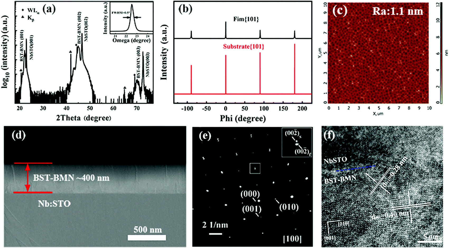 | ||
| Fig. 1 (a) XRD pattern of the BST–BMN thin film. The inset shows the rocking curve of the (002) peak of the BST–BMN thin film. (b) The ϕ scan of the substrate and the BST–BMN thin film in the {101} plane. (c) The surface AFM morphology of the BST–BMN thin film. (d) The cross-sectional SEM morphology of the BST–BMN thin film on the NbSTO substrate. (e) The SAED pattern including both the film and the substrate. Subscripts s and f denote the substrate and the film. (f) The cross-sectional HRTEM image with the interface details. | ||
Plots of the temperature dependence of the relative dielectric permittivity (εr) and the loss tangent (tan![[thin space (1/6-em)]](https://www.rsc.org/images/entities/char_2009.gif) δ) measured at different frequencies in the range of −270 °C and 127 °C are shown in Fig. 2a. It is noteworthy that the generation of the small peaks of the εr and tanδ near 0 °C may be due to the melting of ice. The Curie temperature (TC) appears at around −125 °C, a very low value of which is conducive to the improvement of the BDS, as mentioned above. Moreover, the significant diffuse phase transition (DPT) could be clearly observed at the Curie temperature (TC). As the frequency increases, TC moves to higher temperature and the maximum dielectric permittivity (εm) at TC progressively decreases. These characteristics demonstrate the relaxor behavior of the BST–BMN films, which is mainly originated from the local random electric/elastic fields induced by the addition of the BMN content.9,38 As shown in Fig. 2b, the modified Curie–Weiss relationship was used to calculate the diffuseness degree (γ) of the εr of the investigated system according to the formula: 1/εr − 1/εm = (T − Tm)γ/C, where C denotes the Curie constant. The γ value varied between 1 (for complete ferroelectrics) and 2 (for complete relaxor ferroelectrics).38 The calculated γ value is 1.76, revealing the strong relaxor behavior of the investigated thin films. The absence of any apparent discrepancy and the single peak of the phase distribution in the PFM image further prove the strong relaxor feature of the BST–BMN thin films because of the weak ferroelectric domain present at room temperature, as exhibited in Fig. 2c.44Fig. 2d depicted the room-temperature frequency dependence of the εr and tanδ. The εr reduces slightly as the frequency increases from 100 Hz to 1 MHz, ascribed to the relaxation of dipoles.45 In addition, the tanδ maintains a very low value over the entire test frequency range, which facilitates the acquisition of a large energy storage density. The low tanδ could be attributed to the substitution of Mg2+ and Nb5+ with more chemical stability for Ti4+, which suppressed the electron hopping between Ti4+ and Ti3+.32,46 As a whole, both εr and tanδ display excellent frequency stability, conducive to the frequency stability of the energy storage performances.
δ) measured at different frequencies in the range of −270 °C and 127 °C are shown in Fig. 2a. It is noteworthy that the generation of the small peaks of the εr and tanδ near 0 °C may be due to the melting of ice. The Curie temperature (TC) appears at around −125 °C, a very low value of which is conducive to the improvement of the BDS, as mentioned above. Moreover, the significant diffuse phase transition (DPT) could be clearly observed at the Curie temperature (TC). As the frequency increases, TC moves to higher temperature and the maximum dielectric permittivity (εm) at TC progressively decreases. These characteristics demonstrate the relaxor behavior of the BST–BMN films, which is mainly originated from the local random electric/elastic fields induced by the addition of the BMN content.9,38 As shown in Fig. 2b, the modified Curie–Weiss relationship was used to calculate the diffuseness degree (γ) of the εr of the investigated system according to the formula: 1/εr − 1/εm = (T − Tm)γ/C, where C denotes the Curie constant. The γ value varied between 1 (for complete ferroelectrics) and 2 (for complete relaxor ferroelectrics).38 The calculated γ value is 1.76, revealing the strong relaxor behavior of the investigated thin films. The absence of any apparent discrepancy and the single peak of the phase distribution in the PFM image further prove the strong relaxor feature of the BST–BMN thin films because of the weak ferroelectric domain present at room temperature, as exhibited in Fig. 2c.44Fig. 2d depicted the room-temperature frequency dependence of the εr and tanδ. The εr reduces slightly as the frequency increases from 100 Hz to 1 MHz, ascribed to the relaxation of dipoles.45 In addition, the tanδ maintains a very low value over the entire test frequency range, which facilitates the acquisition of a large energy storage density. The low tanδ could be attributed to the substitution of Mg2+ and Nb5+ with more chemical stability for Ti4+, which suppressed the electron hopping between Ti4+ and Ti3+.32,46 As a whole, both εr and tanδ display excellent frequency stability, conducive to the frequency stability of the energy storage performances.
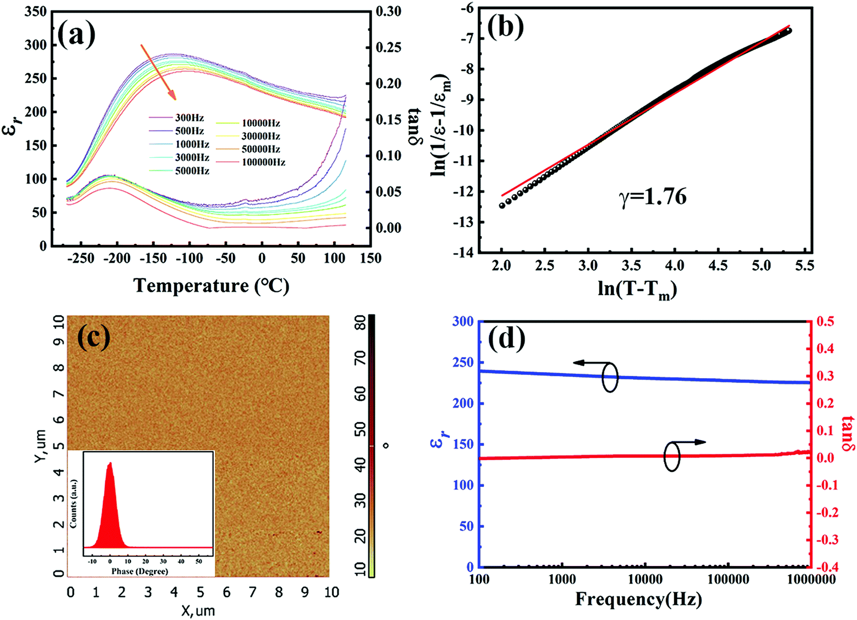 | ||
| Fig. 2 (a) The temperature dependence of the dielectric constant and loss tangent of BST–BMT films. (b) The calculated diffuseness degree of BST–BMN films. (c) PFM phase image of the BST–BMT films. (d) The frequency dependence of the dielectric constant and loss tangent of BST–BMT films measured at room temperature. | ||
The unipolar P–E loops under varied electric fields for BST–BMN films are illustrated in Fig. 3a. All the loops exhibit slim shapes with a relatively small Pr, typical of relaxor ferroelectrics as demonstrated in Fig. 2. The corresponding Pr, ΔP (Pmax − Pr), and Pmax as a function of electric field are displayed in Fig. 3b, where ΔP and Pmax increase dramatically while the Pr raises slightly as the electric field increases. According to eqn (1)–(3), both ΔP and Emax (the maximum electric field applied in films) play a decisive role in enhancing the energy storage density and efficiency. The significant improvement of ΔP with the increase of the electric field contributes to attaining a high energy storage density. Moreover, as shown in Fig. S1 (ESI†), the breakdown strength calculated from the Weibull distribution in the BST–BMN film reaches 5.17 MV cm−1, which is a competitive value compared with other reported perovskite systems.47 In Fig. 3c, the Wrec and η increase from 3.9 J cm−3 and 71.0% to 85.7 J cm−3 and 73.0% respectively as the electric field increases from 500 kV cm−1 to 5 MV cm−1, superior to other lead-free thin film capacitors.47 The improved energy storage performance is linked with the enhanced relaxor property and BDS. On the one hand, when subjected to external electric fields, the weakly coupled polar regions in RFEs would flatten the energy barriers for polarization switching, yielding low hysteresis and high energy storage efficiency.37 On the other hand, the incorporation of Mg2+ and Nb5+ ions with stable valences would suppress the leakage current originating from the valence change of Ti4+, thereby boosting high BDS.32,46 The leakage current density of the BST–BMN film as a function of the electric field is shown in Fig. S2 (ESI†), where the leakage current density was several orders of magnitude lower than those of undoped BST thin films.48,49 Moreover, the incorporation of Mg2+ disrupts the orbital hybridization between Ti 3d states and O 2p states, resulting in the reduced TC and decreased dielectric constant at room temperature, contributing to the enhanced BDS.40 As a result, high energy storage density and efficiency were obtained simultaneously in BST–BMN films.
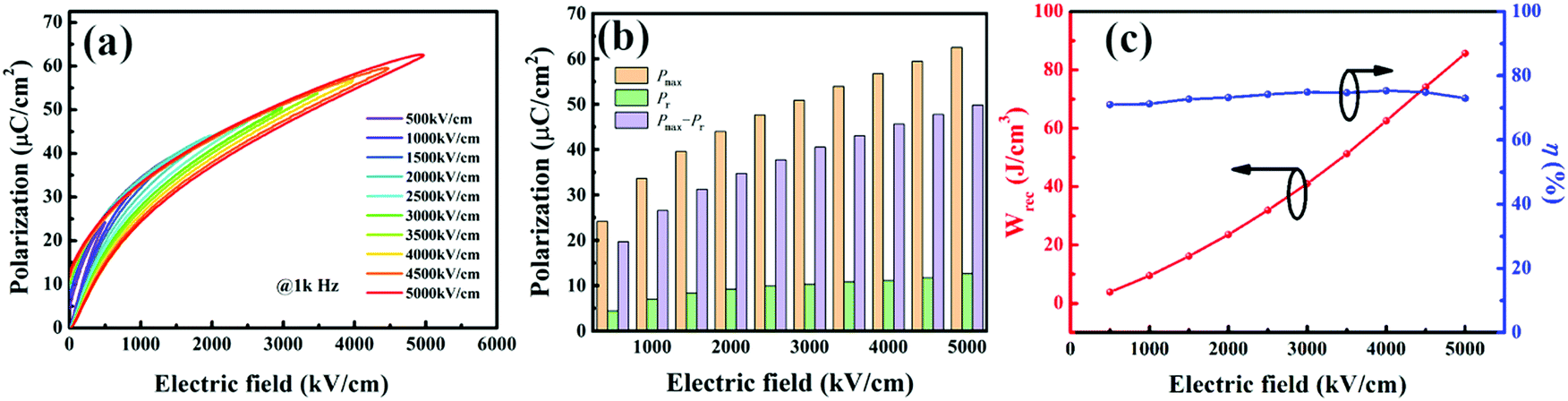 | ||
| Fig. 3 (a) Unipolar P–E loops for BST–BMN films under different electric fields. (b) The summarized Pmax, Pr, and ΔP as a function of electric fields. (c) The calculated energy storage performances of BST–BMN films. | ||
Maintaining stable energy storage performances over a wide temperature range is a key factor for the application of dielectric energy storage materials. Thus, the P–E loops of the BST–BMN films at 2500 kV cm−1 were measured from −100 °C to 100 °C to assess the temperature stability, as shown in Fig. 4a. As can be seen, with the increase of temperature, the shape of the P–E loops had no significant change. The calculated Wrec and η displayed a relatively stable trend with the variation from 28.8 J cm−3 and 74.7% to 32.8 J cm−3 and 70.8% respectively during the measured temperature range. As shown in Fig. 4b, both the variations of Wrec and η were below 13%, demonstrating the excellent temperature stability of the BST–BMN thin film capacitors for actual application. In addition, the investigation of the frequency stability of the BST–BMN thin film is necessary due to its relaxor characteristics.9 As shown in Fig. 4c and d, the Pmax exhibited a declined trend while the Pr increased slightly in the range of 100 Hz to 5 kHz, resulting in the decrease of the Wrec and η from 65.8 J cm−3 and 94.2% to 49.6 J cm−3 and 65.8%, respectively.
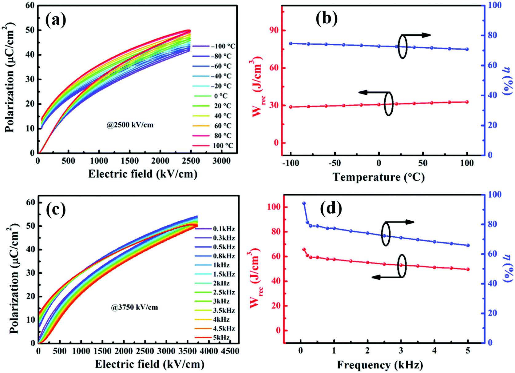 | ||
| Fig. 4 (a) Unipolar P–E loops and (b) corresponding energy storage properties for BST–BMN films as a function of temperature measured at 2500 kV cm−1 and 1 kHz. (c) Unipolar P–E loops and (d) corresponding energy storage properties for BST–BMN films as a function of frequency measured at 3750 kV cm−1. | ||
The outstanding fatigue endurance of the dielectric capacitors is a vital factor for reliable operations during long-term charging–discharging processes. Fig. 5a illustrated the P–E loops after 107 fatigue cycles using 1 kHz triangle signals under the electric field of 2500 kV cm−1. As can be seen, the BST–BMN thin film capacitors exhibited excellent fatigue resistance properties with relatively stable P–E loops, both the Wrec and η of which did not exhibit significant deterioration. Fig. 5b exhibited the calculated value of Wrec and η, which varied from 32.1 J cm−3 and 76.5% to 31.7 J cm−3 and 75.3% respectively with the variation less than 2% after 107 cycles. The strong fatigue resistance properties may be due to the nano-scale domain feature with high dynamics and the suppression of oxygen vacancies originated from the chemical valence fluctuation of Ti4+ through the substitution with chemically more stable Mg2+ and Nb5+ as mentioned above.43
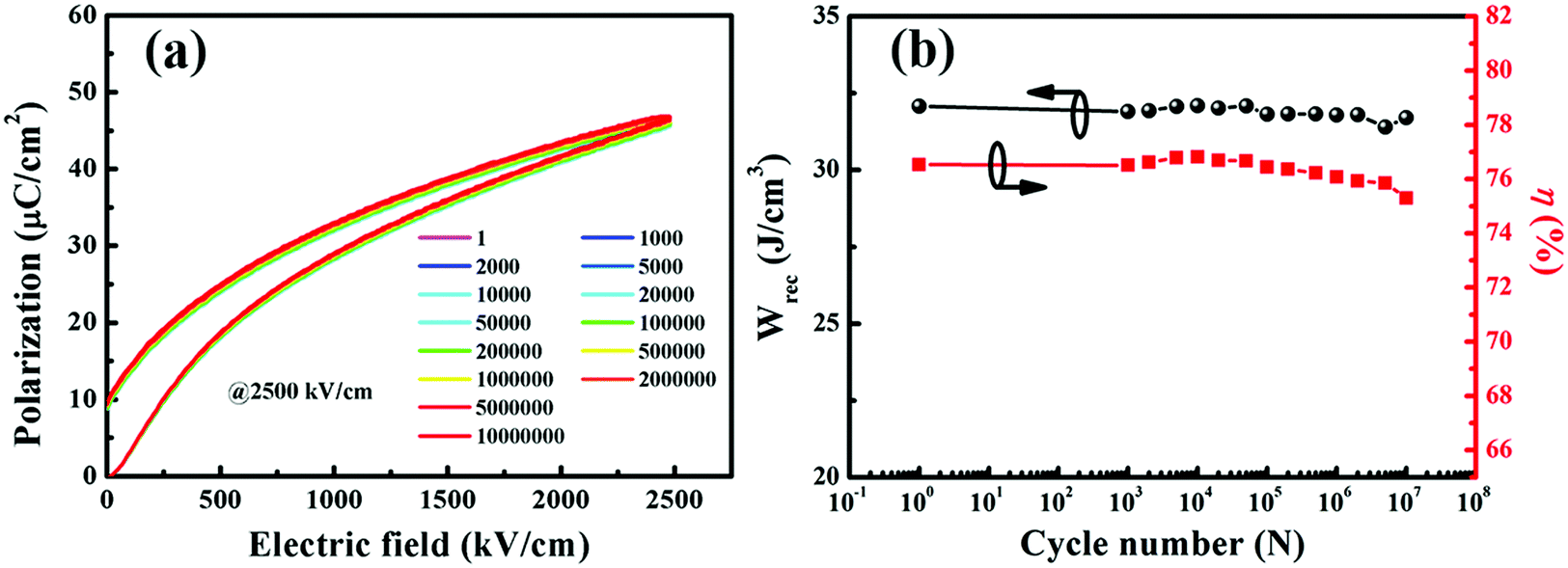 | ||
| Fig. 5 (a) Unipolar P–E loops and (b) corresponding energy storage properties of BST–BMN films as a function of fatigue cycles at 2500 kV cm−1 and 1 kHz. | ||
In addition to the outstanding energy storage density, high power density and fast discharge rate (within the period of 1–1000 ns) are also key factors in evaluating the actual application potential of the thin film capacitors.50 Nowadays, lots of reports have paid attention to the energy storage density which is calculated from the quasi-state P–E loops of the thin film capacitors. However, due to the different measured frequencies between the P–E loops and the pulsed discharge current, high energy storage density does not necessarily guarantee the large power density. Actually, currently it's hard to obtain high energy storage density and power density simultaneously in dielectric capacitors.5 To evaluate the actual discharge performances, the underdamped discharge current curves of BST–BMN films as a function of electric field are displayed in Fig. 6a. As shown, the stored energy can be released quickly within 320 ns, exhibiting great potential for application in pulsed power systems. In addition, the maximum current density (Imax/S) increased from 108 A cm−2 to 185 A cm−2 with the increase in electric field from 750 kV cm−1 to 2250 kV cm−1, as shown in Fig. 6b. The power density (PD), calculated from the formula: PD = EImax/2S (S means the electrode area), presented a trend of linear growth which raised from 41 MW cm−3 to 208 MW cm−3 as the electric field increased from 750 kV cm−1 to 2250 kV cm−1. In this work, the ultrahigh PD of 208 MW cm−3 exhibited a much superior value to commercial BOPP capacitors and many other reported thin film capacitors.51 These excellent charging–discharging properties make BST–BMN films a promising candidate material in energy storage applications.
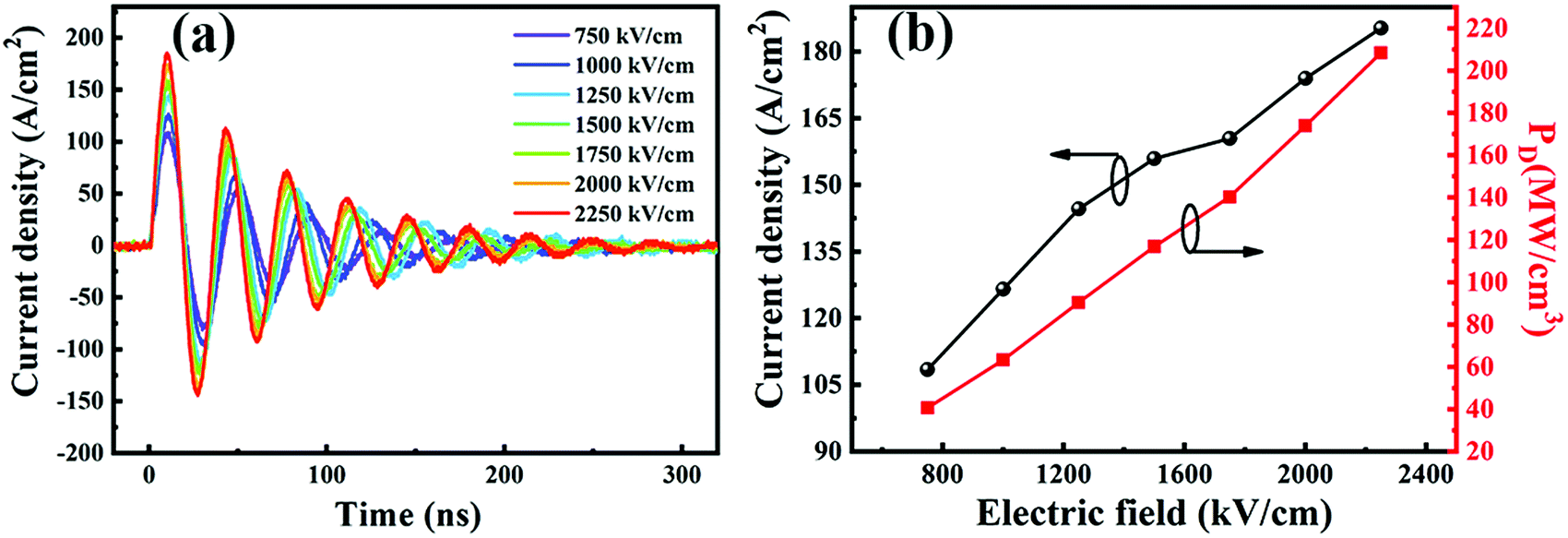 | ||
| Fig. 6 (a) Underdamped discharge waveforms and (b) current density and power density for the BST–BMN thin film capacitors under different electric fields. The load resistor is about 0.5 Ω. | ||
A comparison of the energy storage capabilities of our BST–BMN thin film capacitors with other previously reported representative materials is illustrated in Fig. 7.19,21,22,24,43,52–62 Most of the currently promising thin film materials lie below the diagonal, indicating that the lower Wrec is a general bottleneck that limits the further improvement of energy storage performances of these films. By incorporating non-isovalent ions of BiMg2/3Nb1/3O3, we simultaneously enhance the relaxor behavior and remarkably increase the BDS to boost the Wrec of the BST–BMN film, which makes our materials competitive in energy storage performances. The ultrahigh Wrec and superior η of the BST–BMN thin film capacitors prove their high potential for energy storage applications in power systems. Further research will focus on the improvement of energy storage efficiency without the sacrifice of ultrahigh storage density.
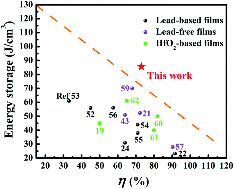 | ||
| Fig. 7 The comparison of the BST–BMN thin films with other reported representative thin film materials. | ||
4. Conclusion
In summary, lead-free 0.88BST–0.12BMN thin films were deposited on NbSTO substrates through pulsed laser deposition technology. An ultrahigh Wrec (85.7 J cm−3) and high η (73.0%) were simultaneously obtained at 5 MV cm−1 in the BST–BMN thin film capacitors, which are superior to many other lead-free thin film capacitors. Excellent fatigue endurance (107 cycles) and thermal stability (−100 °C to 100 °C) were also acquired with the variation of Wrec less than 2% and 13%, respectively. The simultaneously attained ultrahigh BDS and strong relaxor characteristic (γ = 1.76) through the incorporation of non-isovalent ions lead to these remarkable energy storage capabilities. Additionally, the BST–BMN thin film also possessed ultrahigh PD (208 MW cm−3) and fast discharge time (320 ns). This study demonstrates the potential of the BST–BMN thin film capacitors as novel candidates for applications in pulsed power systems and could promote the development of BST-based thin film capacitors with further enhanced BDS and Wrec in the future.Conflicts of interest
There are no conflicts of interest to declare.Acknowledgements
This work was supported by the National Natural Science Foundation of China (Grant No. 51831010). The author Yuzhu Fan would like to give her sincere thanks to Miss. Yichen Wu for her constructive opinions on this manuscript. With her help, the research work was carried out smoothly.References
- W. P. Cao, W. L. Li, X. F. Dai, T. D. Zhang, J. Sheng, Y. F. Hou and W. D. Fei, J. Eur. Ceram. Soc., 2016, 36, 593–600 CrossRef CAS.
- C. Diao, H. Liu, G. Lou, H. Zheng, Z. Yao, H. Hao and M. Cao, J. Alloys. Compd., 2019, 781, 378–384 CrossRef CAS.
- J. Gao, Y. Zhang, L. Zhao, K.-Y. Lee, Q. Liu, A. Studer, M. Hinterstein, S. Zhang and J.-F. Li, J. Mater. Chem. A, 2019, 7, 2225–2232 RSC.
- X. Jiang, H. Hao, S. Zhang, J. Lv, M. Cao, Z. Yao and H. Liu, J. Eur. Ceram. Soc., 2019, 39, 1103–1109 CrossRef CAS.
- N. Liu, R. Liang, Z. Zhou and X. Dong, J. Mater. Chem. C, 2018, 6, 10211–10217 RSC.
- S. Tong, B. Ma, M. Narayanan, S. Liu, R. Koritala, U. Balachandran and D. Shi, ACS Appl. Mater. Interfaces, 2013, 5, 1474–1480 CrossRef CAS PubMed.
- F. Han, G. Meng, F. Zhou, L. Song, X. Li, X. Hu, X. Zhu, B. Wu and B. Wei, Sci. Adv., 2015, 1, e1500605 CrossRef PubMed.
- N. Mohammadian, A. Moshaii, A. Alizadeh, S. Gharibzadeh and R. Mohammadpour, J. Phys. Chem. Lett., 2016, 7, 4614–4621 CrossRef CAS PubMed.
- Y. Wu, Y. Fan, N. Liu, P. Peng, M. Zhou, S. Yan, F. Cao, X. Dong and G. Wang, J. Mater. Chem. C, 2019, 7, 6222–6230 RSC.
- J. Wei, T. Yang and H. Wang, J. Eur. Ceram. Soc., 2019, 39, 624–630 CrossRef CAS.
- Q. Yuan, G. Li, F.-Z. Yao, S.-D. Cheng, Y. Wang, R. Ma, S.-B. Mi, M. Gu, K. Wang, J.-F. Li and H. Wang, Nano Energy, 2018, 52, 203–210 CrossRef CAS.
- J. Yin, Y. Wang, Y. Zhang, B. Wu and J. Wu, Acta Mater., 2018, 158, 269–277 CrossRef CAS.
- H. Yang, F. Yan, Y. Lin, T. Wang, F. Wang, Y. Wang, L. Guo, W. Tai and H. Wei, J. Eur. Ceram. Soc., 2017, 37, 3303–3311 CrossRef CAS.
- H. Qi and R. Zuo, J. Eur. Ceram. Soc., 2019, 39, 2318–2324 CrossRef CAS.
- B. Ma, Z. Hu, R. E. Koritala, T. H. Lee, S. E. Dorris and U. Balachandran, J. Mater. Sci.: Mater. Electron., 2015, 26, 9279–9287 CrossRef CAS.
- M. Acosta, J. Zang, W. Jo and J. Rödel, J. Eur. Ceram. Soc., 2012, 32, 4327–4334 CrossRef CAS.
- Q. Fan, M. Liu, C. Ma, L. Wang, S. Ren, L. Lu, X. Lou and C.-L. Jia, Nano Energy, 2018, 51, 539–545 CrossRef CAS.
- H. Qi and R. Zuo, J. Mater. Chem. A, 2019, 7, 3971–3978 RSC.
- M. H. Park, H. J. Kim, Y. J. Kim, T. Moon, K. D. Kim and C. S. Hwang, Adv. Energy Mater., 2014, 4, 1400610 CrossRef.
- J. Chen, Z. Tang, B. Yang and S. Zhao, Appl. Phys. Lett., 2018, 113, 153904 CrossRef.
- Z. Sun, C. Ma, M. Liu, J. Cui, L. Lu, J. Lu, X. Lou, L. Jin, H. Wang and C. L. Jia, Adv. Mater., 2017, 29, 1604427 CrossRef PubMed.
- M. D. Nguyen, C. T. Q. Nguyen, H. N. Vu and G. Rijnders, J. Eur. Ceram. Soc., 2018, 38, 95–103 CrossRef.
- X. Hao, Y. Wang, J. Yang, S. An and J. Xu, J. Appl. Phys., 2012, 112, 114111 CrossRef.
- X. Wang, L. Zhang, X. Hao, S. An and B. Song, J. Mater. Sci.: Mater. Electron., 2015, 26, 9583–9590 CrossRef CAS.
- J. W. McPherson, K. Jinyoung, A. Shanware, H. Mogul and J. Rodriguez, IEEE Int. Electron Devices, 2003, 50, 1771–1778 CrossRef CAS.
- M. Rabuffi and G. Picci, IEEE Trans. Plasma Sci., 2002, 30, 1939–1942 CrossRef CAS.
- Z. Fang, Y. Chen, X. Li, W. Huang, L. Xia, Y. Shen, G. Wang and X. Dong, J. Eur. Ceram. Soc., 2019, 39, 4817–4823 CrossRef CAS.
- B. Luo, X. Wang, E. Tian, H. Song, H. Wang and L. Li, ACS Appl. Mater. Interfaces, 2017, 9, 19963–19972 CrossRef CAS PubMed.
- Y. Huang, Y. Chen, X. Li, G. Wang, L. Xia, Y. Liu, Y. Shen, J. Shi and X. Dong, J. Eur. Ceram. Soc., 2018, 38, 3861–3866 CrossRef CAS.
- F. Emadi, A. Nemati, M. Hinterstein and E. Adabifiroozjaei, Ceram. Int., 2019, 45, 5503–5510 CrossRef CAS.
- Y. Yu, X. Wang and X. Yao, Ceram. Int., 2013, 39, S335–S339 CrossRef CAS.
- W. Huang, Y. Chen, X. Li, G. Wang, N. Liu, S. Li, M. Zhou and X. Dong, Appl. Phys. Lett., 2018, 113, 203902 CrossRef.
- M. D. Nguyen, C. T. Q. Nguyen, H. N. Vu and G. Rijnders, Curr. Appl. Phys., 2019, 19, 1040–1045 CrossRef.
- S. Cho, C. Yun, Y. S. Kim, H. Wang, J. Jian, W. Zhang, J. Huang, X. Wang, H. Wang and J. L. MacManus-Driscoll, Nano Energy, 2018, 45, 398–406 CrossRef CAS.
- N. Setter and L. Cross, J. Appl. Phys., 1980, 51, 4356–4360 CrossRef CAS.
- A. A. Bokov and Z. G. Ye, J. Mater. Sci., 2006, 41, 31–52 CrossRef CAS.
- H. Pan, F. Li, Y. liu, Q. Zhang, M. Wang, S. Lan, Y. Zheng, J. Ma, L. Gu, Y. Shen, P. Yu, S. Zhang, L. Chen, Y.-H. Lin and C.-W. Nan, Science, 2019, 365, 578–582 CrossRef CAS PubMed.
- J. Li, F. Li, Z. Xu and S. Zhang, Adv. Mater., 2018, 30, e1802155 CrossRef PubMed.
- T. Shi, L. Xie, L. Gu and J. Zhu, Sci. Rep., 2015, 5 Search PubMed.
- M. Deluca, Z. G. Al-Jlaihawi, K. Reichmann, A. M. T. Bell and A. Feteira, J. Mater. Chem. A, 2018, 6, 5443–5451 RSC.
- D. Wang, X. Ke, Y. Wang, J. Gao, Y. Wang, L. Zhang, S. Yang and X. Ren, Phys. Rev. B: Condens. Matter Mater. Phys., 2012, 86, 054120 CrossRef.
- V. V. Shvartsman, J. Dec, T. Łukasiewicz, A. L. Kholkin and W. Kleemann, Ferroelectrics, 2010, 373, 77–85 CrossRef.
- H. Pan, Y. Zeng, Y. Shen, Y.-H. Lin, J. Ma, L. Li and C.-W. Nan, J. Mater. Chem. A, 2017, 5, 5920–5926 RSC.
- F.-Z. Yao, K. Wang, W. Jo, K. G. Webber, T. P. Comyn, J.-X. Ding, B. Xu, L.-Q. Cheng, M.-P. Zheng, Y.-D. Hou and J.-F. Li, Adv. Funct. Mater., 2016, 26, 1217–1224 CrossRef CAS.
- B. Yang, M. Guo, X. Tang, R. Wei, L. Hu, J. Yang, W. Song, J. Dai, X. Lou, X. Zhu and Y. Sun, J. Mater. Chem. C, 2019, 7, 1888–1895 RSC.
- Z. Yao, Z. Song, H. Hao, Z. Yu, M. Cao, S. Zhang, M. T. Lanagan and H. Liu, Adv. Mater., 2017, 29 Search PubMed.
- H. Palneedi, M. Peddigari, G.-T. Hwang, D.-Y. Jeong and J. Ryu, Adv. Funct. Mater., 2018, 28, 1803665 CrossRef.
- J. Qian, C. H. Yang, Y. J. Han, X. S. Sun and L. X. Chen, Ceram. Int., 2018, 44, 20808–20813 CrossRef CAS.
- J. Xie, H. Hao, Z. Yao, L. Zhang, Q. Xu, H. Liu and M. Cao, Ceram. Int., 2018, 44, 5867–5873 CrossRef CAS.
- F. Li, K. Yang, X. Liu, J. Zou, J. Zhai, B. Shen, P. Li, J. Shen, B. Liu, P. Chen, K. Zhao and H. Zeng, Scr. Metall., 2017, 141, 15–19 CrossRef CAS.
- P. Chen, S. Wu, P. Li, J. Zhai and B. Shen, Inorg. Chem. Front., 2018, 5, 2300–2305 RSC.
- X. Hao, Y. Wang, L. Zhang, L. Zhang and S. An, Appl. Phys. Lett., 2013, 102, 163903 CrossRef.
- Z. Hu, B. Ma, R. E. Koritala and U. Balachandran, Appl. Phys. Lett., 2014, 104, 263902 CrossRef.
- Y. Zhao, X. Hao and Q. Zhang, Ceram. Int., 2016, 42, 1679–1687 CrossRef CAS.
- Y. Zhao, X. Hao and Q. Zhang, ACS Appl. Mater. Interfaces, 2014, 6, 11633–11639 CrossRef CAS PubMed.
- Z. Xie, Z. Yue, B. Peng, J. Zhang, C. Zhao, X. Zhang, G. Ruehl and L. Li, Appl. Phys. Lett., 2015, 106, 202901 CrossRef.
- S. S. Won, M. Kawahara, L. Kuhn, V. Venugopal, J. Kwak, I. W. Kim, A. I. Kingon and S.-H. Kim, Appl. Phys. Lett., 2017, 110, 152901 CrossRef.
- Y. Zhang, W. Li, W. Cao, Y. Feng, Y. Qiao, T. Zhang and W. Fei, Appl. Phys. Lett., 2017, 110, 243901 CrossRef.
- H. Pan, J. Ma, J. Ma, Q. Zhang, X. Liu, B. Guan, L. Gu, X. Zhang, Y.-J. Zhang, L. Li, Y. Shen, Y.-H. Lin and C.-W. Nan, Nat. Commun., 2018, 9, 1813 CrossRef PubMed.
- P. D. Lomenzo, C.-C. Chung, C. Zhou, J. L. Jones and T. Nishida, Appl. Phys. Lett., 2017, 110, 232904 CrossRef.
- M. Hoffmann, U. Schroeder, C. Künneth, A. Kersch, S. Starschich, U. Böttger and T. Mikolajick, Nano Energy, 2015, 18, 154–164 CrossRef CAS.
- F. Ali, X. Liu, D. Zhou, X. Yang, J. Xu, T. Schenk, J. Müller, U. Schroeder, F. Cao and X. Dong, J. Appl. Phys., 2017, 122, 144105 CrossRef.
Footnote |
| † Electronic supplementary information (ESI) available. See DOI: 10.1039/c9tc04036f |
| This journal is © The Royal Society of Chemistry 2020 |