
 Open Access Article
 This Open Access Article is licensed under a
 Creative Commons Attribution 3.0 Unported Licence
Elucidating the optical, electronic, and photoelectrochemical properties of p-type copper vanadate (p-Cu5V2O10) photocathodes†
Angang
Song
 ab,
Sean P.
Berglund
a,
Abdelkrim
Chemseddine
a,
Dennis
Friedrich
a,
Fatwa F.
Abdi
a and
Roel
van de Krol
*ab
ab,
Sean P.
Berglund
a,
Abdelkrim
Chemseddine
a,
Dennis
Friedrich
a,
Fatwa F.
Abdi
a and
Roel
van de Krol
*ab
aInstitute for Solar Fuels, Helmholtz-Zentrum Berlin für Materialien und Energie GmbH, Hahn-Meitner-Platz 1, 14109 Berlin, Germany. E-mail: roel.vandekrol@helmholtz-berlin.de
bInstitut für Chemie, Technische Universität Berlin, Straße des 17. Juni 124, 10623 Berlin, Germany
First published on 12th June 2020
Abstract
P-type copper vanadate (Cu5V2O10) photoelectrodes made by spray pyrolysis were developed and evaluated as a potential photocathode material for photoelectrochemical (PEC) water splitting. Using fluorine-doped tin oxide as a substrate, highly phase-pure p-Cu5V2O10 thin films were obtained after annealing at 550 °C for 4 hours in air. Cu5V2O10 has a small bandgap energy in the range of 1.8–2.0 eV, allowing it to absorb visible light and making it potentially interesting for solar water splitting applications. The p-Cu5V2O10 films were characterized by photoelectrochemical techniques in order to provide insight into the critical PEC properties such as the flat-band potential, chemical stability, and incident photon-to-current efficiency (IPCE). The best-performing films showed a photocurrent density of up to 0.5 mA cm−2 under AM1.5 simulated sunlight, and an IPCE value up to 14% for 450 nm light at 0.8 VRHE with H2O2 as an electron scavenger. Despite the narrow band gap and suitable conduction band edge position for PEC H2 production, these p-type films were unstable under constant illumination in aqueous electrolyte (pH 6.8) due to the reduction and dissolution of Cu. Based on our findings, the suitability of Cu5V2O10 as a photocathode material for photoelectrochemical water splitting is critically discussed.
Introduction
The direct storage of solar energy in the form of chemical bonds by photoelectrochemical (PEC) water splitting systems has been regarded as a promising way to replace fossil fuels.1–4 In particular, the reduction of water to produce hydrogen, a clean and sustainable fuel, can be driven by p-type photoelectrodes with suitable band positions. Among all classes of materials investigated as photoelectrodes for solar water splitting, metal oxide semiconductors are particularly attractive mainly due to their relative abundance and low cost as well as their resistance to further oxidation in aqueous solutions. Currently, the highest performing p-type metal oxide photoelectrode is cuprous oxide (Cu2O); a photocurrent as high as ∼10 mA cm−2 and an onset potential as high as 1 V vs. RHE have been reported.5 However, stability remains a major issue. Although it has been demonstrated that the stability can be enhanced by depositing conformal protection layers on top of the Cu2O photocathodes,6 the coating needs to be sufficiently thin (to minimize ohmic losses) and pinhole-free (to prevent degradation). This complicates the deposition process and potentially increases the cost of the photoelectrodes, which further motivates the search for an intrinsically stable p-type photoelectrode. One particular approach is to look for alternative Cu-based ternary metal oxides with a second cation (besides Cu2+ or Cu+) forming the conduction band. This is expected to inhibit the reduction of Cu2+ or Cu+ to Cu at the semiconductor/electrolyte interface, which is the main degradation mechanism in Cu2O.6 Indeed, copper niobates (CuNbO3) and copper ferrites (CuFeO2), in which Nb and Fe d orbitals dominate the conduction band character, show better stability compared to Cu2O.7–11Another possible candidate is copper vanadate (Cu5V2O10), a CuO-based material that is expected to be chemically robust. It has suitable indirect and direct optical band gaps in the range of 1.8–2.0 eV and a moderate absorption coefficient (α ≈ 104 cm−1),12 allowing for the utilization of a significant portion of the solar spectrum to generate photocurrent. However, at present, there are only ∼20 published reports on Cu5V2O10, only 4 of which are relevant to photoelectrochemistry or photocatalysis.12–14 Therefore, many key physical and photoelectrochemical parameters of this material are not yet known. The dominant conductivity type is also still not clear, since both p-type and n-type conductivity have been reported in the literature.15–19 Even less is known about the charge carrier transport properties (e.g., mobility and lifetime), despite Cu5V2O10 being a potentially interesting candidate as a photoelectrode material for solar water splitting.
In this work, we have developed an attractive, low-cost spray pyrolysis recipe for the deposition of thin film Cu5V2O10 photoelectrodes on FTO-coated glass (F-doped SnO2). Our spray pyrolysis method has been demonstrated as a means for homogenously depositing large area photoelectrodes20 that can be integrated with other components in solar fuels devices. The sprayed Cu5V2O10 films show p-type conductivity and have a bandgap of 1.86 eV. We determine the lifetime and mobility of the photogenerated carriers by performing time-resolved microwave conductivity (TRMC) measurements. On the basis of these findings, a first assessment of the suitability of p-type Cu5V2O10 as a photoelectrode material for solar water splitting is provided.
Results and discussion
Structural and chemical characterization
To investigate the structure and chemical composition of the Cu5V2O10 thin film photoelectrodes, X-ray diffraction (XRD), Raman spectroscopy, and XPS measurements were carried out. Details of the experimental methods are included in the ESI.† The X-ray diffractograms of the Cu5V2O10 films are shown in Fig. 1a. The as-deposited Cu5V2O10 film, which was deposited onto the substrate at 300 °C, is structurally amorphous as evident from the XRD pattern (blue curve). The deposition temperature of 300 °C is obviously not enough to crystallize the film. The red curve shows the diffractogram of the Cu5V2O10 thin film with post-deposition annealing at 550 °C for 4 hours in air. It matches very well with the reference pattern (JCPDS no. 33-0504), indicating that the film consists of single phase of Cu5V2O10 with no discernable crystalline impurities. This is also the case for films with various thicknesses (from 50 to 500 nm), as shown in Fig. S1.† The Cu5V2O10 phase has been previously found to crystallize in the monoclinic crystal system (space group P21/c) with the cell parameters of a = 8.3938 Å, b = 6.0659 Å, c = 16.1601 Å and β = 108.0857°.15,21–23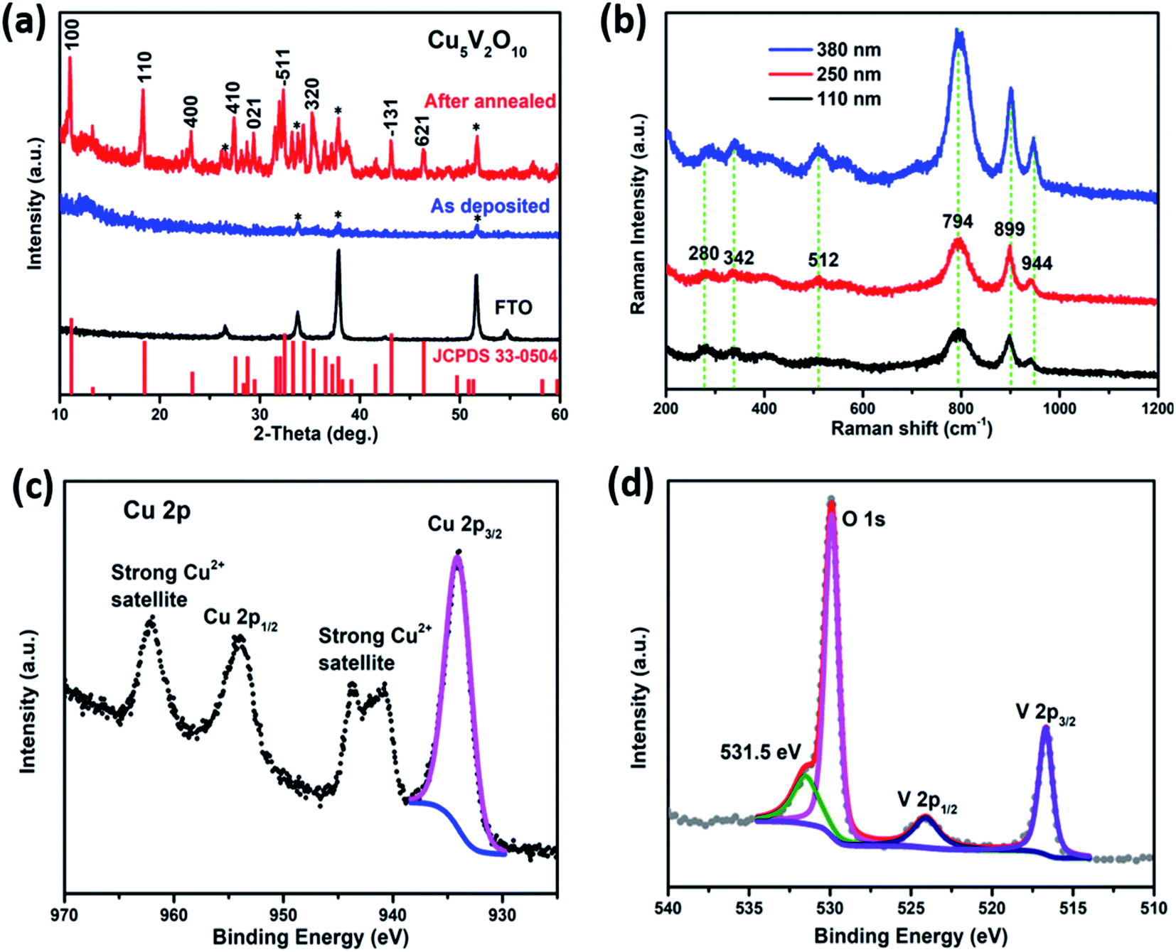 | ||
| Fig. 1 (a) XRD diffractogram for a Cu5V2O10 photocathode synthesized by spray pyrolysis on an FTO substrate. Red vertical lines represent the reference pattern for Cu5V2O10 photoelectrode (PDF no. 33-0504) (b) Raman spectra of the Cu5V2O10 films (annealed at 550 °C for 4 hours in air) with different thicknesses. XPS spectra of (c) Cu 2p, (d) V 2p and O 1s for Cu5V2O10 film. | ||
Fig. 1b shows the Raman spectra of our sprayed Cu5V2O10 samples with different thicknesses. The main Raman bands for Cu5V2O10 centered at ∼794, 899, and 944 cm−1 were observed for all films, which is fully in agreement with reports in the literature.13,14 These scattering peaks are associated with tetrahedral VO4 stretching modes,22 whereas peaks at 280, 342 and 512 cm−1 are assigned to the bending of the same structural motif. Tetrahedral VO4 is the predominant coordination polyhedron in many metal oxides containing V5+.24–26 No Raman peaks for CuO and V2O5 are observed, again demonstrating that our synthesis method yields highly phase-pure thin films of Cu5V2O10.
The core level XPS spectra for Cu 2p, V 2p, and O 1s are compared in Fig. 1c and d. The Cu 2p3/2 spectrum can be deconvoluted into a single peak with a binding energy of 934.1 eV, and strong satellite peaks in the range of 940–945 eV are observed (Fig. 1c). This suggests that the oxidation state of Cu is +2, which is in agreement with the expected formal oxidation states of copper in Cu5V2O10. The V 2p3/2 and V 2p1/2 signal (Fig. 1d) can also be deconvoluted into individual peaks with a binding energies of 516.7 eV and 524.1 eV, respectively, indicating an oxidation state of V5+ based on reports in the literature.27 The O 1s peak is located at 529.9 eV, which is expected for a surface lattice oxygen peak in the film. A minor peak at a higher binding energy of 531.5 eV is also present, which corresponds to surface adsorbed water or hydrogen-bearing groups.28
Morphology characterization
Fig. 2a shows the SEM image of the Cu5V2O10 photoelectrode prepared on FTO glass upon post-deposition annealing. The film consists of nanoparticles with diameters of 100–500 nm. The film shows good overall uniformity, and the average thickness of the film is estimated to be ∼250 nm using 200 mL precursor solution from the cross-section SEM image shown in Fig. 2b. In comparison with previously reported films prepared by inkjet printing,13 these films deposited by spray pyrolysis exhibit a significantly more compact and homogeneous morphology. As a comparison, the SEM images of the bare FTO substrate and as-deposited films are shown in Fig. S2;† the as deposited film consists of larger and round grains with some degree of surface roughness. We also obtained thickness values of ∼110 nm and ∼500 nm (Fig. S3†) from the samples sprayed with 100 mL and 400 mL of the precursor, which indicates a linear relationship between the precursor volume and film thickness. Fig. 2c shows a photograph of a thin film Cu5V2O10 photoelectrode deposited on an FTO-coated glass substrate. The film has a brown color, which appears to be due to the reflected light in the 500–700 nm range, indicating good visible light absorption. Energy dispersive spectroscopy (EDS) was performed on the Cu5V2O10 thin films (see Fig. S4†). The average Cu/(Cu + V) ratio is about (0.70 ± 0.02) measured from several films of different thicknesses, which is consistent with the expected value of 0.71 for Cu5V2O10. EDS mapping was also performed on a representative film area as shown in Fig. S5.† The EDS signals from Cu, V, and O appear to be homogeneously distributed over the entire film area.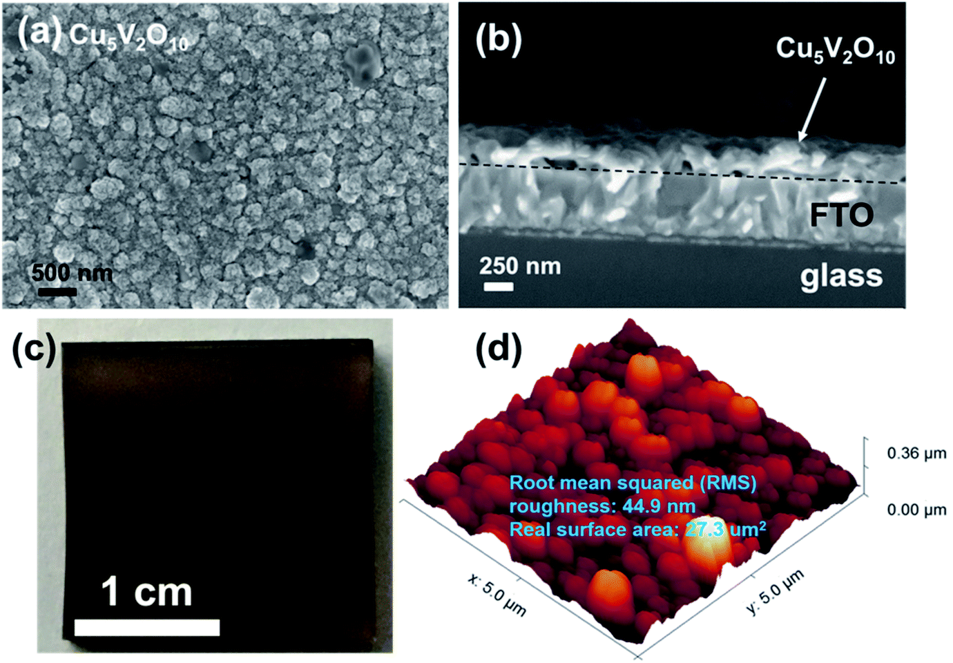 | ||
| Fig. 2 (a) Top-view and (b) cross-section SEM images of a Cu5V2O10 thin film deposited on FTO annealed at 550 °C in air for 4 hours. (c) Photograph of a Cu5V2O10 thin film deposited on an FTO-coated glass substrate. (d) Atomic force microscopy (AFM) image of a ∼250 nm Cu5V2O10 film deposited on an FTO substrate. | ||
The surface roughness of the Cu5V2O10 film was measured using atomic force microscopy (AFM); a representative image on a 5 × 5 μm2 area is shown in Fig. 2d. AFM reveals that the root mean squared (RMS) roughness and real surface area of Cu5V2O10 films are 44.9 nm and 27.3 μm2, respectively. A roughness factor (real surface area divided by geometric surface area) of 1.09 is obtained, which confirms that the film is indeed relatively compact. As a comparison, the AFM image of a bare FTO substrate is shown in Fig. S6,† which shows a roughness factor of 1.06.
Optical properties
Fig. 3a shows the absorptance spectrum of a 250 nm Cu5V2O10 thin film deposited on a quartz substrate as a function of wavelength (absorptance spectra for films with other thicknesses are shown in Fig. S7a†). The absorption increases sharply at approximately 650 nm, which is in agreement with earlier reports.12 The weak absorption tail between 700–800 nm arises from localized ligand field excitation at the Cu2+ (3d9) cations, and therefore does not generate mobile charge carriers.12Fig. 3b shows the absorption coefficient (α) as a function of wavelength, which was calculated from a fit (for each wavelength) of the absorption data of 5 different film thicknesses by using the following equation: α = −ln(TR)/d. TR is the transflectance at a single wavelength and d is the film thickness determined from cross-section SEM. At 450 nm the absorption coefficient for the film is (1.92 ± 0.21) × 104 cm−1 (Fig. S7b†), which corresponds to a light penetration depth of α−1 = 521 nm, i.e., a film thickness of 1.2 μm (2.3 α−1) is required to absorb 90% of the incident light having a wavelength of 450 nm. Tauc analysis was performed on the absorption coefficient spectra to determine the optical bandgaps of Cu5V2O10 as shown in Fig. 3c. Both direct and indirect optical transitions can be discerned. The indirect and direct bandgaps for the Cu5V2O10 thin film are estimated to be 1.9 and 2.1 eV, respectively, which is promising for visible light absorption for a metal oxide photoelectrode material.29,30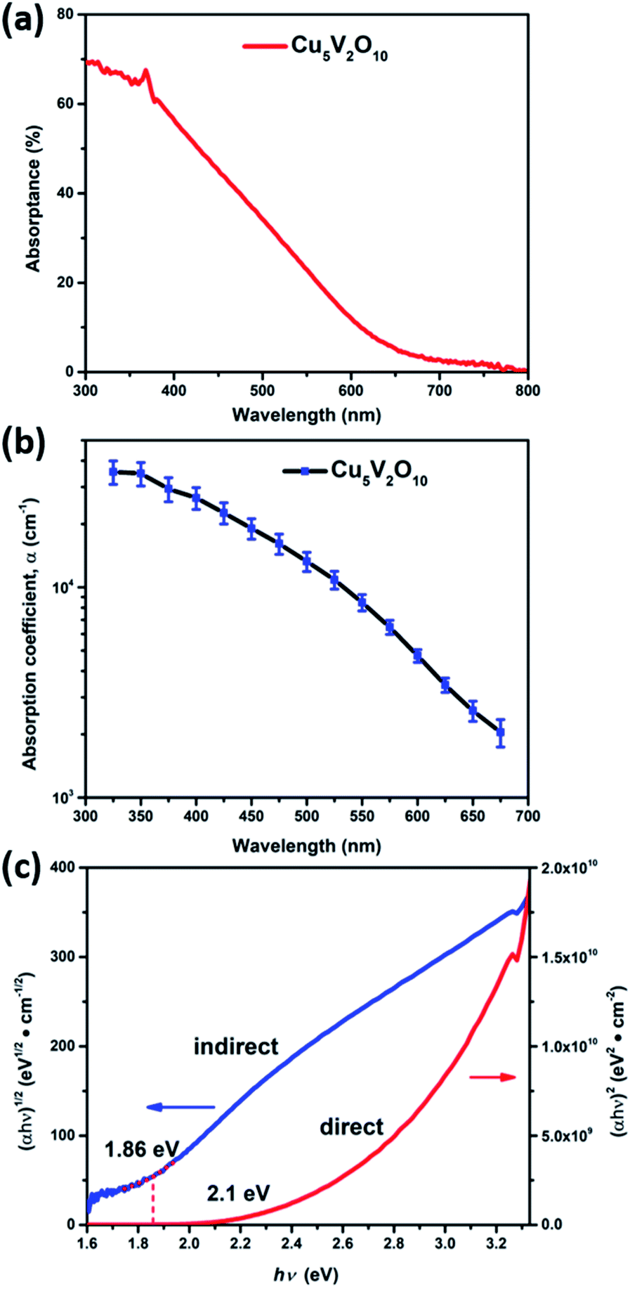 | ||
| Fig. 3 (a) Absorptance spectra and (b) absorption coefficient for 250 nm thick Cu5V2O10 film deposited on quartz substrate. (c) Tauc plots for bandgap analysis of the Cu5V2O10 film. The indirect and direct bandgaps are estimated from inflection point and the intercept of the (αhν)0.5 and (αhν)2 curves with the x-axis, respectively. | ||
Charge carrier transport
The charge carrier transport properties of Cu5V2O10 thin films were investigated using time-resolved microwave conductivity (TRMC) measurements. For this purpose, the films were deposited on quartz substrates, since a non-conducting substrate is necessary for TRMC. However, only moderate TRMC signals can be detected from the Cu5V2O10 thin film, indicating relatively low photoconductivity. Fig. 4a shows the TRMC signal for a 250 nm Cu5V2O10 film under an incident laser pulse intensity of 3 × 1014 cm−2 at four different excitation wavelengths (410, 450, 500, and 500 nm). Mobility values of 1.1–2.3 × 10⁻⁵ cm2 V−1 s−1 were obtained from the peaks of the curves. The decay curves of the Cu5V2O10 sample can be fitted with a power law relationship (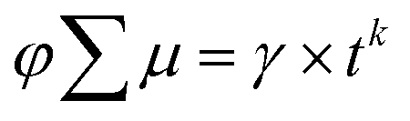 , k = −0.69 ± 0.1, γ = 2.3 × 10⁻¹⁰, t < 1000 ns). The power-law behavior is assigned to the occurrence of trap-limited recombination.31–33 TRMC measurements were also performed under various incident laser pulse intensities as shown in Fig. S8.†Fig. 4b shows the maximum TRMC signal
  versus the incident laser pulse intensity at four different laser wavelengths. With increasing light intensities, the mobility
 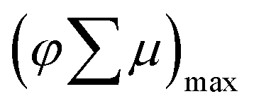 decreases gradually. This can be explained by the occurrence of nongeminate higher order electron–hole recombination. In addition, Fig. 4b shows that there is a clear dependency between the carrier mobility in Cu5V2O10 and the excitation wavelength. We tentatively attribute this to a wavelength-dependent photogeneration yield in Cu5V2O10, similar to what was shown before for hematite.34,35 Indeed, a d–d electronic transition is expected in Cu5V2O10, which in the case of hematite has been suggested to not contribute to the generation of mobile carriers.
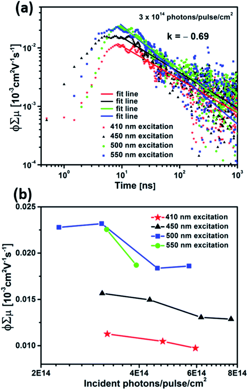 | ||
Fig. 4 (a) TRMC signal under various incident laser pulse intensities for a Cu5V2O10 film synthesized by spray pyrolysis on a quartz substrate at different wavelengths. (b) Maximum TRMC signal  vs. incident laser pulse intensity for Cu5V2O10 films deposited on quartz substrates under different laser wavelengths. vs. incident laser pulse intensity for Cu5V2O10 films deposited on quartz substrates under different laser wavelengths. | ||
The effective lifetime of the charge carriers in Cu5V2O10 films can be defined as the time that it takes for the signal to decrease to 50% of its starting value, and an average value of 30 ns for different excitation wavelengths is found for the Cu5V2O10 film. Based on the effective lifetime and the mobility, one might calculate an “effective” diffusion length of the photoexcited carriers. When doing this, we find a value of 1.3 nm. This value is clearly unrealistic. Even if we account for some surface roughness in our films (Fig. S2b and S3b†), the amount of light absorbed in the first 1.3 nm of the films would lead to negligible photocurrents. As mentioned above, trapping plays an important role in our films, and trapped carriers will have a much lower mobility than (quasi-) free carriers. With this in mind, we attribute the TRMC decay to a decay in mobility, as opposed to a decay in the number of carriers.
While slow carriers might still reach the interface and contribute to the photocurrent, it is reasonable to expect that the chance of recombination increases with the time that the carriers need to reach the interface. Nanostructuring strategies will, therefore, help to reduce the diffusion path lengths and may be needed to improve the charge carrier separation efficiency.
Band positions
The conductivity type and flat band potential of our Cu5V2O10 films were estimated by performing Mott–Schottky analysis. Fig. 5a shows a Mott–Schottky plot for the 250 nm Cu5V2O10 photocathode measured at different frequencies. The negative slopes in the Mott–Schottky curves indicate that the obtained Cu5V2O10 is a p-type semiconductor. In addition, an open-circuit potential (OCP) measurement under chopped AM1.5 illumination confirms the p-type conductivity, i.e., the OCP shifts to a more positive value upon illumination as shown in Fig. S9.† It is worth noting that p-type conductivity for Cu5V2O10 is rarely reported in the literature; n-type Cu5V2O10 is more common.12,13 The p-type conductivity may be caused by the presence of Cu vacancies in the photoelectrode. Cu vacancies have been shown to define the p-type nature of other Cu-based photocathodes, such as CuBi2O4 and CuInS2.36,37 Using eqn (6) in the ESI,† the flat band potential (ϕfb) and acceptor density (NA) can be obtained from the x-axis intercept and the slope of the Mott–Schottky plot, respectively. All Mott–Schottky curves at different frequencies in Fig. 5a intercept the same x-axis value, and the obtained ϕfb value is 1.12 ± 0.02 V vs. RHE, which is consistent with the photocurrent onset potential (∼1.1 V vs. RHE) of the film (vide infra). The frequency dispersion in the Mott–Schottky plot may be due to surface defects or a frequency-dependent dielectric constant; a detailed analysis of this is beyond the scope of this study and the reader is referred to the classic papers of Gomes and Cardon for an in-depth treatment on such phenomena.38,39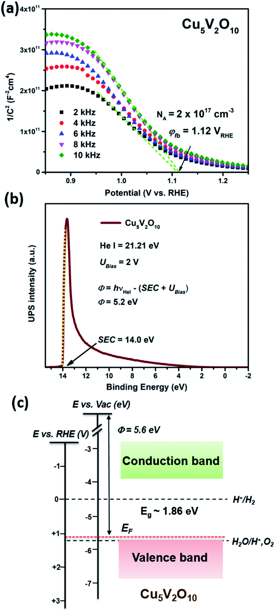 | ||
| Fig. 5 (a) Mott–Schottky plot for a Cu5V2O10 photocathode in 0.3 M K2SO4 and 0.2 M phosphate buffer (pH6.8) at 2 kHz, 4 kHz, 6 kHz, 8 kHz and 10 kHz. (b) UPS cutoff spectra measured with a 2 V bias for ∼250 nm Cu5V2O10 film on FTO. (c) Schematic band diagram of Cu5V2O10 film constructed from UPS and Mott–Schottky measurements. The positions of the valence band, Fermi level EF and the conduction band with respect to the vacuum level, the hydrogen electrode (RHE) potential, as well as water oxidation and reduction potentials are depicted. | ||
It should be noted that the Mott–Schottky curve flattens at the most negative potentials in Fig. 5a. We attribute this to the space charge region becoming large enough for the entire film to be depleted.40 A fully depleted film will act as an insulator with a constant capacitance given by C = ε0εrA/d, where d is the thickness of the film and the other variables are described in the ESI.† Using the plateau values in Fig. 5a and the known value for the film thickness (250 nm), this allows us to calculate the relative permittivity (dielectric constant) of Cu5V2O10 as εr = 520 ± 40 in a frequency range from 4–10 kHz. Note that the β-Cu2V2O7 phase has a similarly high dielectric constant.26 Using this value, the NA of the film is estimated to be about (2.0 ± 0.4) × 1017 cm−3, which is relatively low but well within the range of values commonly observed for metal oxide semiconductors.30,41 Since this low value results in a relatively wide space charge region even at moderate band bending, the space charge region will be insensitive to surface roughness effects and the films can be considered as ‘flat’ for the purpose of the Mott–Schottky analysis. Assuming a typical value of 5 × 1019 cm−3 as the effective density of states at the valence band (NV), the Fermi level is expected to be located ∼110 mV above the valence band maximum (see ESI†).
Fig. 5b shows the secondary electron cut-off UPS spectrum of a 250 nm Cu5V2O10 film measured with a 2 V bias. The work function (difference between the vacuum energy level and Fermi level) can be determined from the high binding energy onset of the secondary electron cut-off.42 The work function is found to be 21.21 − 2 − 14 = 5.21 eV, given that the photon energy of the UV source (He I discharge) is 21.21 eV. Using 4.5 eV vs. vacuum as the reference value for the electrochemical reduction of water (0.0 V vs. RHE),1 this places the work function obtained by UPS at 0.71 V vs. RHE. This is different by ∼0.4 V as compared to the ϕfb value of 1.12 V vs. RHE obtained by the Mott–Schottky analysis. We attribute this to the different sample environment in the two measurements: Mott–Schottky measurement was performed in aqueous electrolyte, whereas UPS measurement was conducted on the surface of the samples in vacuum. As is well known, the work function of a material is extremely sensitive to adsorbate coverage. The drop in work function measured by UPS can also be attributed to the adsorption of carbonaceous species and other atmospheric contaminants on Cu5V2O10 surface, since it has been fully exposed to air before the measurement. The valence band maximum (VBM) position of 0.08 eV below EF is determined by the linear extrapolation of the UPS spectrum at the low binding energy side to the binding energy axis (see Fig. S10†), which is in a good agreement from our previous estimation from Mott–Schottky analysis.
By combining the various parameters that were experimentally determined by UV-vis, Mott–Schottky, and UPS measurements we can now construct a detailed band diagram for Cu5V2O10 photoelectrode. Fig. 5c shows the band diagram of our spray deposited Cu5V2O10 film with respect to the electrochemical redox potentials of the water oxidation (H+, O2/H2O) and reduction (H+/H2) reactions. It shows that the valence band (VB) of Cu5V2O10 is approximately equal to the water oxidation potential. Considering that the Eg is 1.9 eV, we also estimate that the position of conduction band minimum (ECBM) is at about −0.62 V vs. RHE or −3.88 eV vs. Evac, which is more negative than water reduction potential for hydrogen production. In other words, photo-excited electrons in the conduction band of Cu5V2O10 thin films are thermodynamically able to reduce protons to hydrogen.
Photoelectrochemical properties
To investigate the photoelectrochemical performance of Cu5V2O10 films, chopped linear sweep voltammetry (LSV) measurements were conducted under simulated AM1.5 illumination with the Cu5V2O10 photocathode as the working electrode, Pt wire as the counter electrode, and Ag/AgCl as the reference electrode. The measurements were performed in 0.3 M K2SO4 and 0.2 M phosphate buffer (pH 6.8) either with H2O2 added as an electron scavenger to remove the reaction kinetics and surface recombination limitations, or with Ar bubbling (without H2O2) to remove dissolved O2 and test for proton reduction.Fig. 6a shows linear sweep voltammetry (LSV) scans for 250 nm Cu5V2O10 photocathode films measured with Ar bubbling. Photocurrent densities of 0.02 mA cm−2 and 0.01 mA cm−2 were obtained at 0.8 V versus RHE under back and front illumination, respectively. The current spikes are attributed to electron trapping on the photoelectrode's surface, followed by charge recombination.43–45 Overall, moderate photocurrents are achieved. Interestingly, the photocurrent onset potential is relatively positive at ∼1.1 V vs. RHE. This value, i.e., the difference between the thermodynamic reduction potential of water, 0 V vs. RHE, and the photocurrent onset potential, also serves as an indication of the photovoltage generated in the material. For comparison, other promising photocathodes such as CuO, Si, and Cu2ZnSnS4 typically show a photocurrent onset of ∼0.7 V vs. RHE for water reduction,46–51 although similarly high photocurrent onset potentials have recently been reported for Cu2O and CuBi2O4.52,53 Chopped LSV scans with H2O2 were also performed as shown in Fig. 6b. Under optimum conditions (see Fig. S11† for the individual LSV scans for different Cu5V2O10 film thicknesses), we could achieve a photocurrent density of 0.52 mA cm−2 and 0.39 mA cm−2 at 0.8 V versus RHE under back and front illumination, respectively. This is a factor of >10 higher than without H2O2, indicating that the performance of Cu5V2O10 is severely limited by surface reaction kinetics. Chopped LSV scans were also performed for the as deposited Cu5V2O10 photocathode (Fig. S12†); the light current density is barely distinguishable from the dark current density, which shows that the post-deposition annealing step that crystallizes the film is essential in order to get photoactivity.
 | ||
| Fig. 6 Chopped LSV scans for Cu5V2O10 photocathodes synthesized to a thickness of ∼250 nm on FTO measured with Ar bubbling (a) and with H2O2 as an electron scavenger (b) under backside (red line) and frontside illumination (black line). (c) IPCE spectra of Cu5V2O10 measured with H2O2 at a potential of 0.8 V vs. RHE, corresponding integrated photocurrents are represented by the dashed lines. (d) Constant potential measurement at 0.8 V vs. RHE for 250 nm Cu5V2O10 films in the dark and light (AM1.5 irradiation). All measurements were done in 0.3 M K2SO4 and 0.2 M phosphate buffer (pH 6.8). | ||
To get an estimate for the amount of recombination in the films, we compare the measured photocurrents to the photocurrent that can theoretically be generated in a 250 nm thick film (assuming that every absorbed photon yields a photoexcited electron–hole pair and that there is no recombination). The latter can be calculated from the absorption coefficient as a function of wavelength (Fig. 3b) and the AM1.5 solar spectrum. The results, shown in Fig. S13,† reveal that the maximum photocurrent for a 250 nm film is 4.91 mA cm−2. The highest photocurrent observed for our films is 0.52 mA cm−2, which means that ∼89% of the carriers recombine.
To gain additional information about the wavelength-dependence of the quantum efficiency of Cu5V2O10 photocathodes, we measured the incident photon-to-current conversion efficiency (IPCE) and calculated the absorbed photon-to-current efficiency (APCE) either with H2O2 or with Ar bubbling. Fig. 6c shows the IPCE spectra of the Cu5V2O10 film measured at 0.8 V versus RHE with H2O2 under back and front illumination. The onset of the IPCE was 680 nm and it increases gradually toward shorter wavelengths. The Cu5V2O10 film produces IPCE values of <15% for all wavelengths. The highest IPCE values of 14% and 10% were measured at around 400 nm under back and front illumination, respectively. The predicted AM1.5 photocurrent density (JAM1.5) of the photocathodes can be estimated by multiplying the IPCE values by the AM1.5 solar photon flux and subsequently integrating this for wavelengths below 700 nm according to eqn (5).† Integrating these spectra with the standard AM 1.5G solar spectrum yielded predicted photocurrent densities of 0.54 mA cm−2 and 0.37 mA cm−2 for Cu5V2O10 photocathode measured under back and front illumination, respectively. These values are consistent with the photocurrent densities of 0.52 and 0.39 mA cm−2 observed for the chopped LSV measurements at the same potential (Fig. 6b). IPCE spectra of Cu5V2O10 were also measured without H2O2 (Fig. S14 in the ESI†); in this case, the IPCE values remain lower than 1% for all wavelengths. Fig. S15† shows the APCE spectra for Cu5V2O10 photocathode measured with H2O2 at 0.8 V vs. RHE under front and back illumination. The APCE shows the highest values in the region between 500–600 nm, which is consistent with the TRMC data in Fig. 4b. Overall, the low quantum efficiency is consistent with the very short effective carrier diffusion length, indicating that majority of the photoexcited carriers recombine before they even reach the interfacemodest AM1.5 photocurrents and the extensive trapping we observed from the TRMC measurements.
We note that the photoelectrochemical performance, both the AM1.5 photocurrent and the IPCE, of Cu5V2O10 under back illumination is always larger than that under front illumination. Considering that our films are compact and that the absorption coefficient is high enough to have a non-constant light intensity profile across the film thickness, we can attribute this difference to the transport distance of electrons and holes in Cu5V2O10. Under front illumination, holes have to traverse the entire thickness of the film, while electrons only need to travel a short distance. The situation is reversed under back illumination. Therefore, we can conclude that electron transport is more efficient, and hole transport is the limiting factor in Cu5V2O10. The poor hole transport properties may seem surprising in view of the fact that Cu5V2O10 is a p-type semiconductor, in which holes are the majority carriers. We attribute this to the fact that the film has a rather low acceptor density (∼2 × 1017 cm−3) and shows near-insulating behavior when fully depleted (vide supra). This also suggests that p-type doping might be a promising strategy to improve the performance of these film; this strategy has been successfully applied to a variety of n-type photoelectrodes, most notably Fe2O3 and BiVO4.54,55
In order to investigate the stability of the Cu5V2O10 photocathodes, the photocurrent density was measured as a function of time at a fixed constant potential of 0.8 V vs. RHE under back illumination. The photocurrents show a fast decaying feature at the initial stage after illumination, which is often observed for unstable semiconductors (see Fig. S16†). The photocurrent density decreases by 85% within 10 min. This indicates extensive photocorrosion, which is a common problem for Cu-based photocathodes.41,45,56 On the other hand, Cu5V2O10 can transfer photo-generated electrons into the electrolyte much more efficiently when H2O2 is present. The results are shown in Fig. 6d. The photocurrent density shows relatively good stability in the first 20 min and decreases by only 14%. After 20 min, however, it rapidly degrades to about 13% of its original value within 120 min and the illuminated area of the Cu5V2O10 electrode has completely disappeared (see the inset of Fig. 6d). We integrated the photocurrent density of the Cu5V2O10 photocathode over time to obtain the total charge that passed for the red curve of Fig. 6d. The obtained value, 0.021 mmol cm−2, is over 7.6 times larger than the total charge needed to reduce all cations including Cu2+, V5+, in the composite photocathode (0.0028 mmol cm−2). Thus, about (7.6 − 1)/7.6 = 87% of the photocurrent density went toward H2O2 reduction, while 13% of the charge was presumably used to dissolve the film. The occurrence of photocorrosion even in the presence of an efficient electron scavenger indicates that p-Cu5V2O10 is intrinsically unstable in aqueous solutions and that suitable protection layers are needed for this material. In contrast, the stability of n-type copper vanadate photoanodes, such as α-CuV2O6, β-Cu2V2O7, γ-Cu3V2O8, and Cu11V6O26 appears less problematic. Although protection layers may still be required for practical applications, several reports have demonstrated stabilities of several hours for n-type copper vanadates.12,26,57,58 To compare the oxidation states changes in Cu5V2O10 electrode, XPS spectra of the sample after 1 hour of PEC measurements (i.e., before the films were completely dissolved) were recorded (Fig. S17†). The Cu 2p peaks clearly shift toward lower binding energies after the PEC measurement, and fitting of the peaks show that the surface now contains a larger amount of Cu+ species (Cu2+![[thin space (1/6-em)]](https://www.rsc.org/images/entities/char_2009.gif) :Cu+ ratio of 1) (Fig. S17a†). This confirms that the Cu2+ at the surface of the Cu5V2O10 photocathode suffers cathodic photo-corrosion during PEC measurement in aqueous electrolyte, which is consistent with the fact that the electrochemical reduction potentials for Cu2+ are more positive than the reduction potential for H+. This photoelectrochemical reduction of Cu2+ is clearly a relatively fast reaction, since it cannot be prevented even with the presence of an electron scavenger (i.e., H2O2) in our electrolyte. The XPS spectra for the O 1s and V 2p regions of PEC tested area are shown in Fig. S17b.† A higher proportion of the adsorbed hydroxyl species after PEC measurement is evidenced from the O 1s peaks, as a result of the exposure to the aqueous electrolyte solutions. In the V 2p spectra, the peaks shifted to higher binding energy, suggesting that PEC measurement resulted in an increase in oxidation state of V to perhaps (partially) compensate the charge imbalance (i.e., due to the reduction of copper). The simultaneous oxidation of the co-cation of Cu has also been observed for CuBi2O4 photocathodes, in which the Bi 4f5/2 and 4f7/2 peaks shifted to higher binding energy after PEC experiments.30,59
:Cu+ ratio of 1) (Fig. S17a†). This confirms that the Cu2+ at the surface of the Cu5V2O10 photocathode suffers cathodic photo-corrosion during PEC measurement in aqueous electrolyte, which is consistent with the fact that the electrochemical reduction potentials for Cu2+ are more positive than the reduction potential for H+. This photoelectrochemical reduction of Cu2+ is clearly a relatively fast reaction, since it cannot be prevented even with the presence of an electron scavenger (i.e., H2O2) in our electrolyte. The XPS spectra for the O 1s and V 2p regions of PEC tested area are shown in Fig. S17b.† A higher proportion of the adsorbed hydroxyl species after PEC measurement is evidenced from the O 1s peaks, as a result of the exposure to the aqueous electrolyte solutions. In the V 2p spectra, the peaks shifted to higher binding energy, suggesting that PEC measurement resulted in an increase in oxidation state of V to perhaps (partially) compensate the charge imbalance (i.e., due to the reduction of copper). The simultaneous oxidation of the co-cation of Cu has also been observed for CuBi2O4 photocathodes, in which the Bi 4f5/2 and 4f7/2 peaks shifted to higher binding energy after PEC experiments.30,59
Conclusions
In this work we have identified the optoelectronic and PEC properties of a p-type Cu5V2O10 photocathode synthesized by a scalable spray pyrolysis method, including bandgap, absorption coefficient, band positions, carrier mobility, flat band potential. Our study shows that the valence and conduction bands of Cu5V2O10 are nearly ideally positioned for PEC water splitting as they straddle the water oxidation and reduction potentials and allow for visible light absorption, which makes Cu5V2O10 a promising candidate to act as a top absorber layer in a dual absorber device for high-efficiency water reduction. However, the moderate absorption coefficient prevents it from absorbing a significant portion of the AM1.5 spectrum. Moreover, extensive trapping will likely prevent the photogenerated carriers from reaching the interface in these spray-deposited p-type films. Bare p-type Cu5V2O10 is also limited by its poor chemical stability, since we observed extensive photo-corrosion, even in the presence of H2O2 as an electron scavenger. Further strategies such as the application of HER catalysts, protection layers, and interfacial layers can be used to improve the photoconversion efficiency of p-type Cu5V2O10 photocathodes. Nevertheless, given the severity of the carrier transport and stability limitations, it will be a major challenge to address both of these limitations at the same time. Efforts might be better spent in developing other complex metal oxide photocathodes, such as CuBi2O4, CaFe2O4, and CuFeO2.60,61Author contributions
The manuscript was written through contributions of all authors. All authors have given approval to the final version of the manuscript.Conflicts of interest
There are no conflicts to declare.Acknowledgements
Angang Song thanks the China Scholarship Council for financial support (File no. 201607040078). We thank Christian Höhn for assistance with XPS and UPS measurements.References
- R. van de Krol and M. Grätzel, Photoelectrochemical hydrogen production, Springer, 2012 Search PubMed.
- M. G. Walter, E. L. Warren, J. R. McKone, S. W. Boettcher, Q. Mi, E. A. Santori and N. S. Lewis, Chem. Rev., 2010, 110, 6446–6473 CrossRef CAS PubMed.
- T. Bak, J. Nowotny, M. Rekas and C. C. Sorrell, Int. J. Hydrogen Energy, 2002, 27, 991–1022 CrossRef CAS.
- B. Alfaifi, H. Ullah, S. Alfaifi, A. Tahir and T. Mallick, Photoelectrochemical solar water splitting: from basic principles to advanced devices, Veruscript Functional Nanomaterials, 2018, 2, BDJOC3 CrossRef.
- J. Luo, L. Steier, M.-K. Son, M. Schreier, M. T. Mayer and M. Grätzel, Nano Lett., 2016, 16, 1848–1857 CrossRef CAS PubMed.
- A. Paracchino, V. Laporte, K. Sivula, M. Grätzel and E. Thimsen, Nat. Mater., 2011, 10, 456–461 CrossRef CAS PubMed.
- Y. J. Jang and J. S. Lee, ChemSusChem, 2019, 12, 1835–1845 CrossRef CAS PubMed.
- U. A. Joshi, A. M. Palasyuk and P. A. Maggard, J. Phys. Chem. C, 2011, 115, 13534–13539 CrossRef CAS.
- M. S. Prévot, N. Guijarro and K. Sivula, ChemSusChem, 2015, 8, 1359–1367 CrossRef PubMed.
- I. Sullivan, B. Zoellner and P. A. Maggard, Chem. Mater., 2016, 28, 5999–6016 CrossRef CAS.
- K. Rajeshwar, M. K. Hossain, R. T. Macaluso, C. Janáky, A. Varga and P. J. Kulesza, J. Electrochem. Soc., 2018, 165, H3192–H3206 CrossRef CAS.
- C.-M. Jiang, G. Segev, L. H. Hess, G. Liu, G. Zaborski, F. M. Toma, J. K. Cooper and I. D. Sharp, ACS Appl. Mater. Interfaces, 2018, 10, 10627–10633 CrossRef CAS PubMed.
- P. Newhouse, D. Boyd, A. Shinde, D. Guevarra, L. Zhou, E. Soedarmadji, G. Li, J. B. Neaton and J. M. Gregoire, J. Mater. Chem. A, 2016, 4, 7483–7494 RSC.
- T. Kawada, S. Hinokuma and M. Machida, Catal. Today, 2015, 242, 268–273 CrossRef CAS.
- T. Hillel and Y. Ein-Eli, J. Power Sources, 2013, 229, 112–116 CrossRef CAS.
- J. Dai, M. Lai, R. M. LaFollette and D. Reisner, ECS Trans., 2011, 33, 3–9 CAS.
- Y. Sakurai, H. Ohtsuka and J. i. Yamaki, J. Electrochem. Soc., 1988, 135, 32–36 CrossRef CAS.
- Z. He, C. Lin, W. Cheng, A. Okazawa, N. Kojima, J.-i. Yamaura and Y. Ueda, J. Am. Chem. Soc., 2010, 133, 1298–1300 CrossRef PubMed.
- J. Ko, S. H. Kang, H.-W. Cheong, Y. S. Yoon, J. Ko, S. H. Kang, H.-W. Cheong and Y. S. Yoon, J. Korean Ceram. Soc., 2019, 56, 233–255 CrossRef CAS.
- I. Y. Ahmet, Y. Ma, J.-W. Jang, T. Henschel, B. Stannowski, T. Lopes, A. Vilanova, A. Mendes, F. F. Abdi and R. van de Krol, Sustainable Energy Fuels, 2019, 3, 2366–2379 RSC.
- M. Eguchi, A. Komamura, T. Miura and T. Kishi, Electrochim. Acta, 1996, 41, 857–861 CrossRef CAS.
- R. Shannon and C. Calvo, Acta Crystallogr., Sect. B: Struct. Crystallogr. Cryst. Chem., 1973, 29, 1338–1345 CrossRef CAS.
- L. Denisova, Y. F. Kargin, N. Belousova, N. Galiakhmetova and V. Denisov, Russ. J. Inorg. Chem., 2019, 64, 725–728 CrossRef CAS.
- C.-M. Jiang, M. Farmand, C. H. Wu, Y.-S. Liu, J. Guo, W. S. Drisdell, J. K. Cooper and I. D. Sharp, Chem. Mater., 2017, 29, 3334–3345 CrossRef CAS.
- T. Kawada, T. Tajiri, H. Yamashita and M. Machida, Catal. Sci. Technol., 2014, 4, 780–785 RSC.
- A. Song, A. Chemseddine, I. Y. Ahmet, P. Bogdanoff, D. Friedrich, F. F. Abdi, S. P. Berglund and R. van de Krol, Chem. Mater., 2020, 32, 2408–2419 CrossRef CAS.
- S. K. Pilli, T. E. Furtak, L. D. Brown, T. G. Deutsch, J. A. Turner and A. M. Herring, Energy Environ. Sci., 2011, 4, 5028–5034 RSC.
- R. Sankari, M. Ehara, H. Nakatsuji, Y. Senba, K. Hosokawa, H. Yoshida, A. De Fanis, Y. Tamenori, S. Aksela and K. Ueda, Chem. Phy. Lett., 2003, 380, 647–653 CrossRef CAS.
- M. Zhang, Y. Ma, D. Friedrich, R. van de Krol, L. H. Wong and F. F. Abdi, J. Mater. Chem. A, 2018, 6, 548–555 RSC.
- S. P. Berglund, F. F. Abdi, P. Bogdanoff, A. Chemseddine, D. Friedrich and R. van de Krol, Chem. Mater., 2016, 28, 4231–4242 CrossRef CAS.
- J. E. Kroeze, T. J. Savenije and J. M. Warman, J. Am. Chem. Soc., 2004, 126, 7608–7618 CrossRef CAS PubMed.
- M. Kuno, D. P. Fromm, H. F. Hamann, A. Gallagher and D. J. Nesbitt, J. Chem. Phys., 2000, 112, 3117–3120 CrossRef CAS.
- A. Barzykin and M. Tachiya, J. Phys. Chem. B, 2002, 106, 4356–4363 CrossRef CAS.
- A. Kay, M. Fiegenbaum-Raz, S. Müller, R. Eichberger, H. Dotan, R. van de Krol, F. F. Abdi, A. Rothschild, D. Friedrich and D. A. Grave, Adv. Funct. Mater., 2019, 1901590 Search PubMed.
- D. Hayes, R. G. Hadt, J. D. Emery, A. A. Cordones, A. B. Martinson, M. L. Shelby, K. A. Fransted, P. D. Dahlberg, J. Hong and X. Zhang, Energy Environ. Sci., 2016, 9, 3754–3769 RSC.
- F. M. Courtel, A. Hammami, R. Imbeault, G. Hersant, R. W. Paynter, B. t. Marsan and M. Morin, Chem. Mater., 2010, 22, 3752–3761 CrossRef CAS.
- F. Wang, W. Septina, A. Chemseddine, F. F. Abdi, D. Friedrich, P. Bogdanoff, R. van de Krol, S. D. Tilley and S. P. Berglund, J. Am. Chem. Soc., 2017, 139, 15094–15103 CrossRef CAS PubMed.
- F. Cardon and W. P. Gomes, J. Phys. D: Appl. Phys., 1978, 11, L63–L67 CrossRef CAS.
- W. P. Gomes and F. Cardon, Prog. Surf. Sci., 1982, 12, 155–215 CrossRef CAS.
- R. van de Krol, A. Goossens and J. Schoonman, J. Electrochem. Soc., 1997, 144, 1723 CrossRef CAS.
- A. Song, P. Plate, A. Chemseddine, F. Wang, F. F. Abdi, M. Wollgarten, R. van de Krol and S. P. Berglund, J. Mater. Chem. A, 2019, 7, 9183–9194 RSC.
- M. Helander, M. Greiner, Z. Wang and Z. Lu, Appl. Surf. Sci., 2010, 256, 2602–2605 CrossRef CAS.
- Y. Nakabayashi, M. Nishikawa and Y. Nosaka, Electrochim. Acta, 2014, 125, 191–198 CrossRef CAS.
- Y.-H. Choi, K. D. Yang, D.-H. Kim, K. T. Nam and S.-H. Hong, Mater. Lett., 2017, 188, 192–196 CrossRef CAS.
- W. Septina, R. R. Prabhakar, R. Wick, T. Moehl and S. D. Tilley, Chem. Mater., 2017, 29, 1735–1743 CrossRef CAS.
- M. G. Kast, L. J. Enman, N. J. Gurnon, A. Nadarajah and S. W. Boettcher, ACS Appl. Mater. Interfaces, 2014, 6, 22830–22837 CrossRef CAS PubMed.
- D. Kang, T. W. Kim, S. R. Kubota, A. C. Cardiel, H. G. Cha and K.-S. Choi, Chem. Rev., 2015, 115, 12839–12887 CrossRef CAS PubMed.
- A. A. Dubale, W.-N. Su, A. G. Tamirat, C.-J. Pan, B. A. Aragaw, H.-M. Chen, C.-H. Chen and B.-J. Hwang, J. Mater. Chem. A, 2014, 2, 18383–18397 RSC.
- C. G. Morales-Guio, S. D. Tilley, H. Vrubel, M. Grätzel and X. Hu, Nat. Commun., 2014, 5, 3059 CrossRef PubMed.
- H. Kumagai, T. Minegishi, Y. Moriya, J. Kubota and K. Domen, J. Phys. Chem. C, 2014, 118, 16386–16392 CrossRef CAS.
- G. Ma, T. Minegishi, D. Yokoyama, J. Kubota and K. Domen, Chem. Phys. Lett., 2011, 501, 619–622 CrossRef CAS.
- L. Pan, Y. Liu, L. Yao, R. Dan, K. Sivula, M. Grätzel and A. Hagfeldt, Nat. Commun., 2020, 11, 318 CrossRef CAS PubMed.
- R. Gottesman, A. Song, I. Levine, M. Krause, A. T. M. N. Islam, D. Abou-Ras, T. Dittrich, R. van de Krol and A. Chemseddine, Adv. Funct. Mater., 2020, 1910832 CrossRef CAS.
- I. Cesar, A. Kay, J. A. Gonzalez Martinez and M. Grätzel, J. Am. Chem. Soc., 2006, 128, 4582–4583 CrossRef CAS PubMed.
- Y. Liang, T. Tsubota, L. P. A. Mooij and R. van de Krol, J. Phys. Chem. C, 2011, 115, 17594–17598 CrossRef CAS.
- A. Song, P. Bogdanoff, A. Esau, I. Y. Ahmet, I. Levine, T. Dittrich, T. Unold, R. van de Krol and S. P. Berglund, ACS Appl. Mater. Interfaces, 2020, 12, 13959–13970 CrossRef CAS PubMed.
- L. Zhou, Q. Yan, J. Yu, R. J. R. Jones, N. Becerra-Stasiewicz, S. K. Suram, A. Shinde, D. Guevarra, J. B. Neaton, K. A. Persson and J. M. Gregoire, Phys. Chem. Chem. Phys., 2016, 18, 9349–9352 RSC.
- M. A. Lumley and K.-S. Choi, Chem. Mater., 2017, 29, 9472–9479 CrossRef CAS.
- D. Kang, J. C. Hill, Y. Park and K.-S. Choi, Chem. Mater., 2016, 28, 4331–4340 CrossRef CAS.
- M. S. Prévot, X. A. Jeanbourquin, W. S. Bourée, F. Abdi, D. Friedrich, R. van de Krol, N. Guijarro, F. Le Formal and K. Sivula, Chem. Mater., 2017, 29, 4952–4962 CrossRef.
- D. K. Lee, D. Lee, M. A. Lumley and K.-S. Choi, Chem. Soc. Rev., 2019, 48, 2126–2157 RSC.
Footnote |
| † Electronic supplementary information (ESI) available. See DOI: 10.1039/d0ta04250a |
| This journal is © The Royal Society of Chemistry 2020 |