
10 cm2 nonfullerene solar cells with efficiency over 10% using HxMoO3-assisted growth of silver electrodes with a low threshold thickness of 4 nm†
Xueshi
Jiang
,
Lulu
Sun
,
Wen
Wang
,
Fei
Qin
,
Cong
Xie
,
Lin
Hu
and
Yinhua
Zhou
 *
*
Wuhan National Laboratory for Optoelectronics, Huazhong University of Science and Technology, Wuhan 430074, China. E-mail: yh_zhou@hust.edu.cn
First published on 20th November 2019
Abstract
In this study, we report 10 cm2 nonfullerene solar cells with power conversion efficiency of 10.24%. The demonstration of the large-area cells is based on the HxMoO3-assisted growth of two silver electrodes, namely, the ultrathin-transparent electrode (on the top) and opaque electrode (at the bottom). The device structure has the configuration glass/HxMoO3/opaque Ag (70 nm)/active layer/HxMoO3/ultrathin Ag (8 nm)/MoO3. The chemically reactive HxMoO3 could react with silver oxide during the growth of the initial few nanometers of silver, as inferred from X-ray spectroscopy measurements. The reaction increases the nucleus sites that assist the continuous and uniform growth of the silver films. The percolation threshold thickness of conductive ultrathin Ag films on HxMoO3 can be as low as 4 nm. The root-mean-square surface roughness of opaque silver (70 nm) grown on the HxMoO3 surface is as low as 1.06 nm. HxMoO3 facilitates the growth of uniform, continuous and smooth silver films that enable the efficient large-area nonfullerene organic solar cells.
Introduction
In recent years, organic solar cells (OSCs) have attracted considerable attention for its advantages of light weight, solution processibility, and good mechanical flexibility. Great efforts have been made on material design, interface optimization, and mechanisms of charge transfer and dissociation to improve the device performance.1–10 Recently, the development of low bandgap non-fullerene acceptors with acceptor–donor–acceptor (A–D–A) structure has significantly facilitated the improvement in power conversion efficiency (PCE).11,12 To date, PCE values over 16% have been reported in small-area devices (about 0.1 cm2).8 Despite the efficiency of small-area devices being rapidly improved, the PCE of large-area devices (>2 cm2) still lags far behind their small-area counterparts.Compared with their silicon and III–V counterparts, organic semiconductors have lower dielectric constant and charge carrier mobility. These properties limit the optimum thickness of the organic active layers in the OSCs typically to about 100 nm to minimize the charge recombination. Such a thin layer is highly vulnerable to the surface roughness of the substrates. Spikes or aggregates on the substrates would result in large current leakage or shortage.13,14 The possibility of defect appearance on the substrates is exponential to the substrate area.15,16 Hence, large-area OSCs generally tend to electrically leak or short, resulting in poor performance. In the literature, thick active layer materials (up to 500 nm) with high crystallinity have been reported, which can tolerate the aggregates or spikes on the substrates to facilitate the demonstration of large-area solar cells.17 Similarly, it has also been demonstrated that the tandem structure of OSCs can improve the device yield because the entire thickness of multilayers (including two active layers and an interconnecting layer combination) is larger than that of a single active layer, which increases the defect tolerance and improves the device yield.18 The above strategies focus on the thickness increase of the layers between the two electrodes to increase the defect tolerance. However, the recently developed high-performance nonfullerene active layers typically have an optimum thickness of 100 nm.8,19 Another strategy to enhance the device yield and efficiency is to reduce the aggregation on the electrode surface by improving the growth of the bottom electrode. However, it is still challenging to fabricate uniform, smooth bottom electrodes with large area.
The silver electrode is a commonly used electrode in OSCs. It has high conductivity and can also show high transmittance when its thickness is small (around 10 nm). However, silver generally grows in the Volmer–Weber mode (‘island’ mode) when the thickness of Ag is below its percolation threshold.20 The ‘island’ growth mode will result in aggregation with a rough surface. To inhibit the island formation, strategies of tuning the deposition conditions21,22 and surface properties23–29 have been reported in the literature. Polyethyleneimine (PEI), gold, and germanium have been reported to facilitate the continuous growth of silver films and reduce the percolation threshold thickness.29–31 These material surfaces provide physical nuclei for silver deposition due to the physical interaction with the silver. Thus far, strategies of producing chemical reactive surfaces for silver deposition have not been reported in the literature.
Herein, we report the silver growth on a chemical reactive hydrogen molybdenum bronze (HxMoO3) surface. The percolation threshold thickness of silver can reach as low as 4 nm on HxMoO3. The surface roughness of thick opaque silver (70 nm) is 1.06 nm on HxMoO3, which is much lower than that deposited on a glass or MoO3 surface. The chemical reaction occurs between HxMoO3 and silver oxides during the thermal evaporation and results in a high density of nuclei. HxMoO3 simultaneously functions as an efficient hole-transporting layer (HTL), which is an appropriate combination with an Ag film as an efficient hole-collecting electrode. On the smooth surface of the bottom silver electrode, we could fabricate a 10 cm2 monolithic OSC with efficiency of 10.2%.
Results and discussion
Fig. 1a shows the device architecture: glass/HxMoO3/70 nm Ag/ZnO/PM6:IT-4F/HxMoO3/ut-Ag/MoO3 (30 nm), where ut-Ag represents the ultrathin silver film. HxMoO3 was used to assist the growth of the bottom thick Ag electrode (70 nm) for obtaining a smooth surface and the top transparent ut-Ag electrode for higher transmittance and electrical conductivity. HxMoO3 has a high work function of 5.4 eV and functions as an efficient HTL between the active layer and top ut-Ag electrode.32 Moreover, HxMoO3 is amorphous and there is no clear peak in the X-ray diffraction test (Fig. S1†). The cell is top-illuminated. The MoO3 film on top of the ut-Ag electrode was used as the antireflective layer (ARL). PM6:IT-4F was used as the photoactive layer.33Fig. 1b shows the patterns of 10 cm2 (2 cm × 5 cm) solar cells. To reduce the series resistance and improve the charge collection of the large-area cells, an Ag line on the ut-Ag electrode around the effective device area was deposited. Fig. 1c shows a picture of a fabricated 10 cm2 top-illuminated cell with the patterning in Fig. 1b. Optical simulation was performed to find the optimum thickness of each layer (Fig. S3†). Following the simulation results, the combination of 8–9 nm Ag and 40–50 nm MoO3 delivers high current density that is consistent with the measured high transmittance (Fig. S2†). Both small-area and large-area solar cells were fabricated. Reference devices with architecture glass/ITO/ZnO/PM6:IT-4F/MoO3 or HxMoO3/Ag were also fabricated (Table S2†). Current–voltage (I–V) curves of the 0.1 cm2 and 10 cm2 devices are shown in Fig. 1d. The photovoltaic parameters of the devices are summarized in Table 1. The best 0.1 cm2 device exhibits a short-circuit current density (JSC) of 20.08 mA cm−2, open-circuit voltage (VOC) of 0.85 V, FF of 0.75, and PCE of 12.75%. The 10 cm2 device exhibits a JSC of 18.36 mA cm−2, VOC of 0.84 V, and FF of 0.67, yielding a PCE of 10.24%. This is the first time that PCE exceeds 10% in the condition of device area > 2 cm2 compared with previous results reported in the literature, particularly for a monolithic device.15,34–42 Compared with the 0.1 cm2 cell, the PCE of the large-area cell decreases from 12.75% to 10.24%, while the VOC is similar. The PCE decrease is mainly due to the decrease in JSC (from 20.08 to 18.36 mA cm−2) and FF (from 0.75 to 0.67). The decrease in JSC and FF is associated with the increase in series resistance (Rs, from 0.7 to 2.0 ohm cm2) and decrease in shunt resistance (Rsh, from 1054 to 526 ohm cm2). The increase in Rs is mainly due to the large sheet resistance of the top electrode. The decrease in Rsh is possibly related to the film defects in the large-area active layers. We have also fabricated the large-area cells on ITO electrodes. The 10 cm2 device on an ITO substrate showed electrical short (Fig. S4†). Furthermore, we also tested the stability of the solar cells with the new device structure under continuous illumination (Fig. S5†). The PCE of the cell remains at 75% of the original after 680 h light illumination, while that of the reference cell (glass/ITO/ZnO/PM6:IT-4F/MoO3/Ag) remains at 48% of the original after the same illumination period.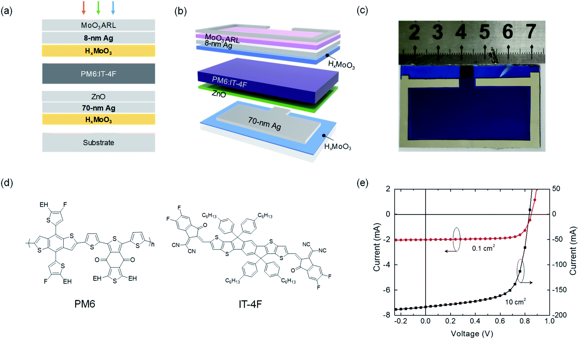 | ||
| Fig. 1 (a) Schematic device structure of a top-illuminated large-area organic solar cell where both bottom thick and top ultrathin silver electrodes were grown with the assistance of HxMoO3 surface. (b) Schematic patterns of the fabricated 10 cm2 (2 cm × 5 cm) solar cells. (c) A picture of a fabricated 10 cm2 top-illuminated cell. (d) Chemical structures of PM6 and IT-4F. ‘EH’ in PM6 denotes 2-ethylhexyl. (e) Current–voltage (I–V) characteristics under AM 1.5G illumination of 0.1 cm2 and 10 cm2 solar cells. | ||
| Area [cm2] | Electrode | J SC [mA cm−2] | V OC [V] | FF | PCE [%] |
|---|---|---|---|---|---|
| 0.1 | ut-Ag + ARL | 20.08 (20.26) | 0.85 (0.85) | 0.75 (0.73) | 12.75 (12.57) |
| 10 | ut-Ag + ARL | 18.36 (18.27) | 0.84 (0.83) | 0.67 (0.65) | 10.24 (9.91) |
The successful demonstration of the 10 cm2 cells is attributed to the smooth surface of the bottom thick Ag electrode and good optoelectronic properties of the top ut-Ag transparent electrode. Both electrodes were deposited on HxMoO3. Fig. 2a–c show the atomic force microscope (AFM) images of the 70 nm Ag deposited on glass, glass/HxMoO3, and typically used glass/ITO electrodes. The ITO film on the glass substrate shows a height variation of about 20 nm with a root-mean-square (RMS) surface roughness of 3.63 nm. Some dots with height over 40 nm are also observed on the ITO surface. These high dots could induce defects on the thin active layers. Hence, typically, it is challenging to obtain high-performance large-area solar cells on ITO electrodes. For the 70 nm Ag film directly deposited on the glass substrate, the surface is also rough with a RMS value of 3.33 nm (Fig. 2b). When a layer of HxMoO3 was inserted between glass and Ag, a smooth surface can be obtained with a RMS roughness value of 1.06 nm. The sectional height variation is typically less than 10 nm.
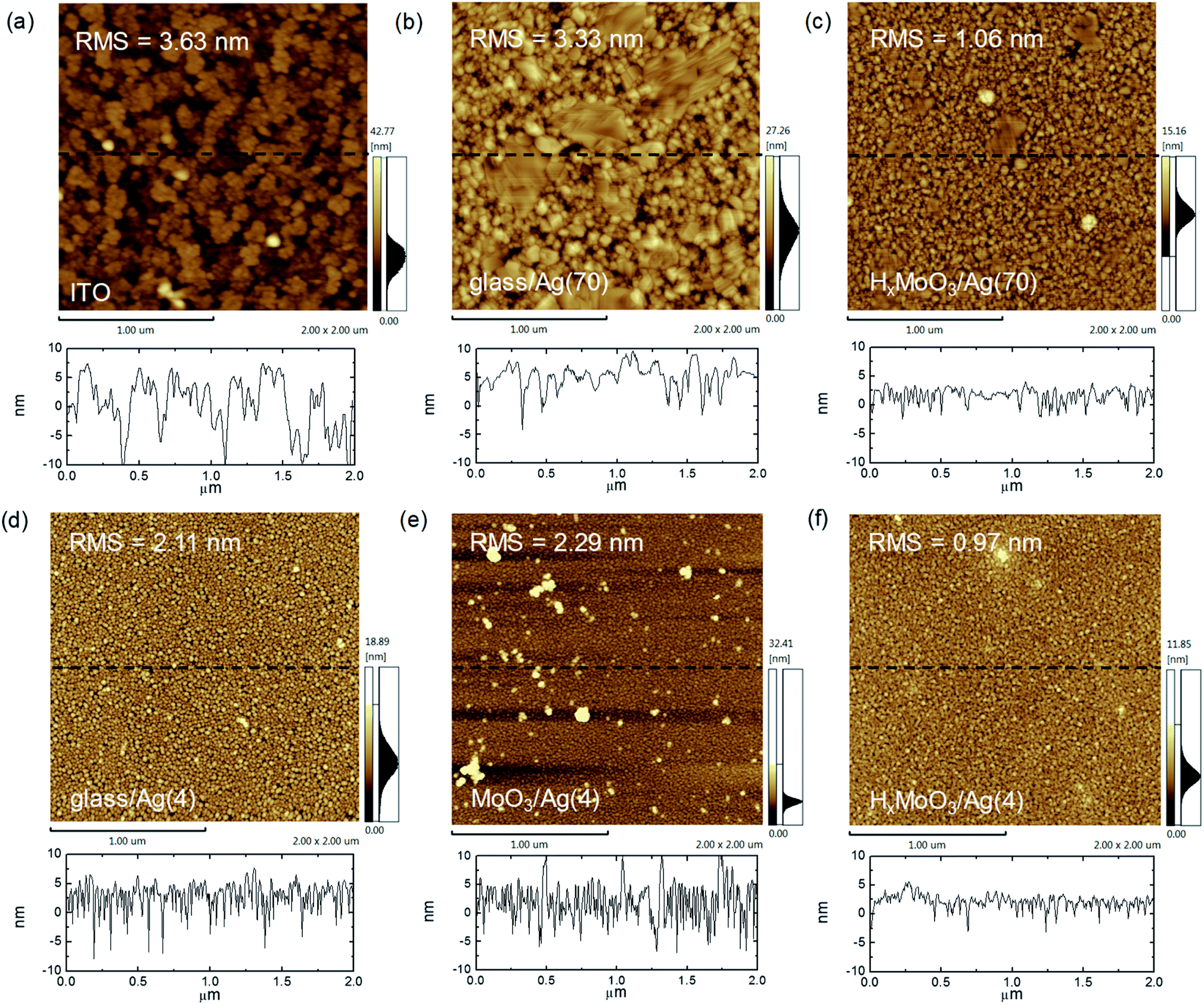 | ||
| Fig. 2 Atomic force microscope (AFM) images of (a) ITO, 70 nm Ag on: (b) glass; (c) HxMoO3. AFM images of 4 nm Ag on: (d) glass; (e) MoO3; (f) HxMoO3. Sectional height distribution indicated with a dash line in (a–f) is below each AFM image. | ||
To understand why a smoother Ag film can be obtained on HxMoO3 than on glass, it is important to investigate the growth behavior of the very first few nanometers of the silver layer. Therefore, we deposited a 4 nm thick silver film on HxMoO3, MoO3 and glass, respectively. In the 4 nm Ag film deposited on glass, large-sized (20–30 nm) silver nanoparticles loosely stacked in the film (Fig. 2d). In the film deposited on MoO3, the Ag nanoparticles become denser, and some large-sized aggregates can be seen (Fig. 2e). In the Ag film deposited on HxMoO3, the film is more continuous and uniform (Fig. 2f). The RMS surface roughness of the 4 nm Ag film on HxMoO3 is 0.97 nm, which is lower than that of the 4 nm Ag deposited on glass (2.11 nm) and MoO3 (2.29 nm). The Ag film deposited on HxMoO3 shows smaller height variation than that on glass and MoO3, according to the sectional height distribution. The results also confirm that HxMoO3 can assist the uniform growth of the ultrathin Ag film at the very first few nanometers. Similar behavior is also observed for the 6 nm and 8 nm Ag films (Fig. S6 and S7†).
In addition to the surface morphology, optical and electrical measurements are powerful to investigate the growth behavior of the ultrathin silver (ut-Ag) films. Fig. 3a shows optical transmittance spectra of Ag films with different thicknesses (2, 4, 8 nm) deposited on the surface of glass, MoO3, and HxMoO3. Broad absorption can be observed for these films deposited on MoO3 and glass, which result from the localized surface plasmon resonance (LSPR) of discontinuous thin metal films.43,44 For the films deposited on HxMoO3, the plasmon absorption only appears when the nominal thickness of ut-Ag is 2 nm. When the nominal thickness increases to 4 nm, the ut-Ag films on HxMoO3 does not show plasmon absorption. This suggests that the percolation thickness of Ag films can be reduced to between 2 and 4 nm. This is the minimum among the reported results in the literature for films deposited by thermal evaporation. Fig. 3b shows the optical transmittance of the 4 nm Ag film deposited on different substrates, with 30 nm MoO3 as the antireflective layer (ARL). With the ARL, the transmittance of the ut-Ag film on HxMoO3 is improved in the longer wavelength region. The average transmittance in the range of 300–1000 nm is about 80%. For the films deposited on MoO3 and glass, the deposition of the ARL doesn't improve their transmittance in the long wavelength region because these films still suffer from strong plasmon resonance absorption.
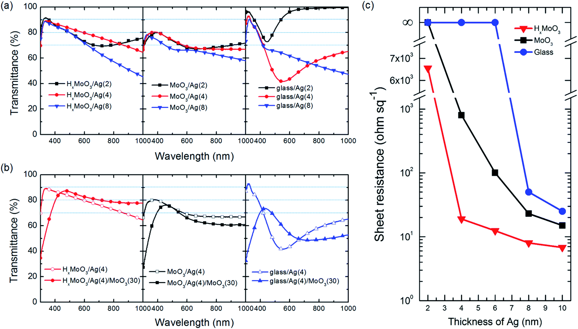 | ||
| Fig. 3 (a) Optical transmittance of different-thickness ut-Ag deposited on different surface: HxMoO3 (left), MoO3 (middle) and glass (right). (b) Optical transmittance of 4 nm ut-Ag with ARL deposited on HxMoO3 (left), MoO3 (middle) and glass (right). ARL is 30 nm MoO3. (c) Sheet resistance of different-thickness ut-Ag on different surfaces (HxMoO3, MoO3, and glass). | ||
The uniform and continuous growth of the ut-Ag film can be also evaluated from the conductivity measurements. Discontinued islands would result in poor electrical conductance. Fig. 3c shows the evolution of the sheet resistance of ut-Ag on HxMoO3, MoO3 and glass as the thickness changes. The sheet resistance of ut-Ag deposited on glass is beyond the measurement limit until the thickness increases to 8 nm, following which a high sheet resistance of 50 ohm sq−1 is obtained. For the samples deposited on both MoO3 and HxMoO3, the sheet resistance values are measurable when the thickness is 4 nm. The sheet resistance of MoO3/Ag (4 nm) is around 1000 ohm sq−1, which is much higher than that of HxMoO3/Ag (4 nm) (19 ohm sq−1). The rapid decrease in the sheet resistance of ut-Ag deposited on HxMoO3 from 6532 ohm sq−1 (2 nm, Fig. 3c) to 19 ohm sq−1 (4 nm) also suggests that the percolation threshold thickness is between 2 nm and 4 nm. This is consistent with the optical transmittance results. The sheet resistance of the ut-Ag film deposited on HxMoO3 can be further reduced to 6.8 ohm sq−1 on further increasing the thickness up to 10 nm. These results suggest that HxMoO3 could assist the growth of ut-Ag films that simultaneously achieve low sheet resistance at a small film thickness. The thin continuous films show high optical transmittance and no plasmon absorption at a nominal thickness of 4 nm.
To understand why HxMoO3 can assist the uniform growth of ultrathin Ag, X-ray photoelectron spectroscopy (XPS) was performed on HxMoO3 before and after the deposition of a 4 nm Ag layer. The evolution of the Mo 3d core level spectrum before and after Ag deposition is shown in Fig. 4a. For the pristine HxMoO3 film, the peaks located at 233.6 eV and 236.7 eV are assigned to Mo6+, corresponding to the 3d3/2 and 3d5/2 core level components.45,46 Another doublet at 232.5 eV and 235.8 eV is assigned to Mo5+.46–48 The ratio of Mo5+![[thin space (1/6-em)]](https://www.rsc.org/images/entities/char_2009.gif) :Mo6+ was calculated to be 1:3.34. After the deposition of ut-Ag on HxMoO3, the content of Mo5+ reduced and the Mo5+:Mo6+ ratio becomes 1:9.90. The evolution tendency of O 1s (Fig. 4b) is in accordance with the result of the Mo 3d spectrum. The peak at 530.9 eV ascribed to the typical Mo–O bond49 and the another peak at 532.1 eV assigned to Mo5+–OH49 were observed in the XPS O 1s spectrum of pristine HxMoO3. The ratio of Mo–OH:Mo–O decreases from 1:1.33 to 1:1.55 after the ut-Ag deposition.
:Mo6+ was calculated to be 1:3.34. After the deposition of ut-Ag on HxMoO3, the content of Mo5+ reduced and the Mo5+:Mo6+ ratio becomes 1:9.90. The evolution tendency of O 1s (Fig. 4b) is in accordance with the result of the Mo 3d spectrum. The peak at 530.9 eV ascribed to the typical Mo–O bond49 and the another peak at 532.1 eV assigned to Mo5+–OH49 were observed in the XPS O 1s spectrum of pristine HxMoO3. The ratio of Mo–OH:Mo–O decreases from 1:1.33 to 1:1.55 after the ut-Ag deposition.
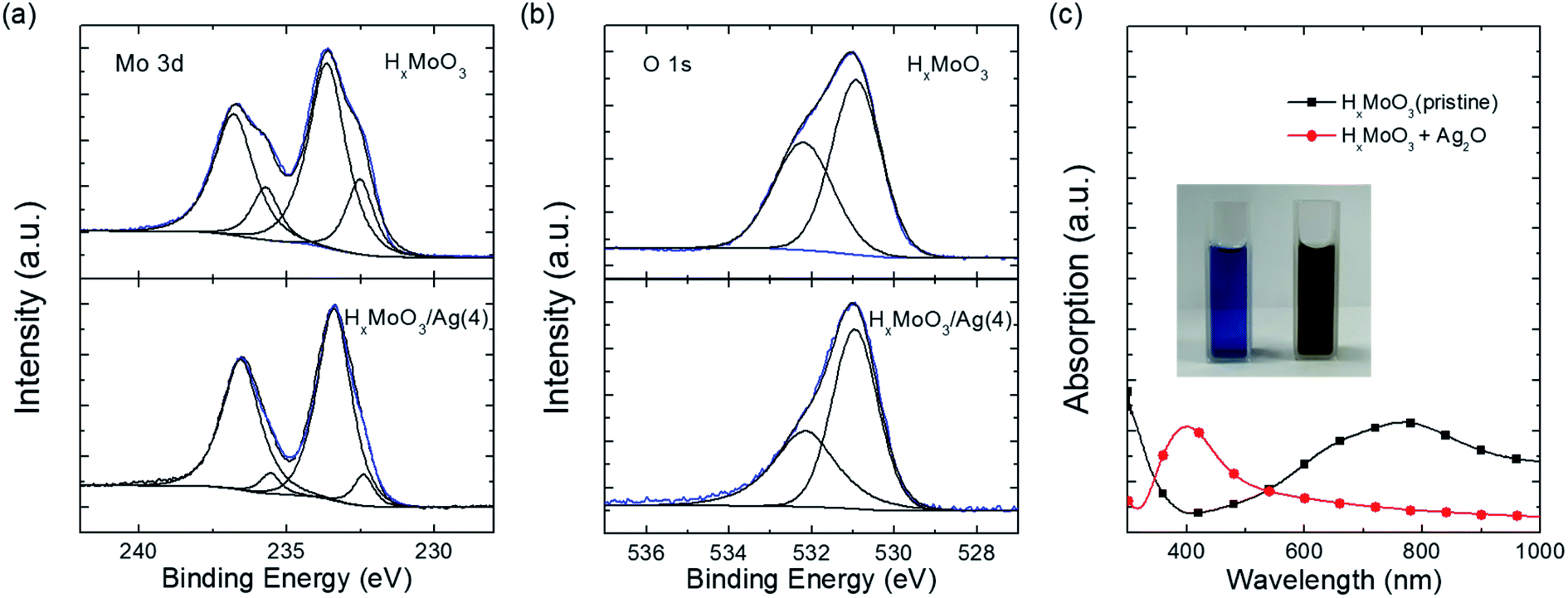 | ||
| Fig. 4 (a) XPS Mo 3d spectra and (b) XPS O 1s spectra of pristine HxMoO3 film (upper) and HxMoO3 film after deposition of 4 nm Ag (bottom). (c) Optical absorption spectra of HxMoO3 (blue) and HxMoO3 + Ag2O (dark yellow), and inset shows a photographic image of the two solutions. | ||
During the deposition, the Mo5+ component is oxidized to Mo6+. We assume that silver oxide is the possible oxidant. XPS measurements were performed on the thick evaporated Ag film. The O 1s spectrum is shown in Fig. S8.† The only peak located at 532.3 eV is assigned to the dissolved oxygen50,51 instead of adsorbed oxygen (528.1–528.5 eV) after thermal evaporation. This suggests the existence of oxygen during the evaporation process. Thus, the silver oxide could form in the presence of oxygen and high temperature of thermal evaporation.
Furthermore, we confirmed the chemical reaction between silver oxide and HxMoO3. The blue color of pristine HxMoO3 in aqueous solution turned dark yellow after adding silver oxide powder. The color change occurs within a few seconds after the addition of silver oxide. The absorption spectra of the HxMoO3 solution before and after adding silver oxide are shown in Fig. 4c. A broad asymmetric absorption band between 500 and 1000 nm is observed in the pristine HxMoO3, related to the intervalence-charge transfer from Mo5+ to Mo6+.52 The absorption band vanishes after silver oxide addition, which suggests the decrease in Mo5+ content. The observed phenomenon is in accordance with the XPS results. Additionally, the absorption peak at 400 nm appears, which is ascribed to the typical plasmon resonance absorption of Ag nanoparticles.53–55 Therefore, the reaction occurs according to the following equation:
| Mo5+ + AgOx → Mo6+ + Ag | (1) |
With this rapid reaction, the active sites yield high nuclei density at the initial stage of the deposition that assists the uniform growth of ut-Ag. This explains why ut-Ag can show a lower percolation threshold thickness and lower sheet resistance compared with the films deposited on glass and MoO3. The continuous growth of silver films at the initial deposition stage further yields a smooth surface of thick opaque silver films.
Conclusions
In summary, we have demonstrated 10 cm2 nonfullerene solar cells with power conversion efficiency over 10%. This is the first report where the power conversion efficiency exceeds 10% when the device area is larger than 2 cm2. The demonstration of the efficient large-area cells is based on the growth of silver electrodes on chemically reactive HxMoO3. The HxMoO3 surface provides a high nuclei density of the uniform and continuously grown silver films. This indicates that the percolation threshold thickness of conductive ultrathin Ag films on HxMoO3 can be as low as 4 nm, and the root-mean-square surface roughness of opaque silver film (70 nm) can be as low as 1.06 nm grown on HxMoO3, which is significantly reduced compared to those of the silver films grown on glass or MoO3 surface.The strategy of producing a chemically reactive surface for silver deposition effectively reduces the surface roughness and improves optical and electrical properties of silver films. Importantly, HxMoO3 is also a very efficient hole-transporting layer in these devices. The proposed surface of HxMoO3 is very unique for organic solar cells. The introduction of chemical reactive sites assisting the growth of ultrathin metals will also inspire the exploration of new transparent electrodes for device applications.
Experimental section
Materials
PM6 and IT-4F were purchased from Solarmer Materials Inc., Beijing. The ZnO sol–gel solution was prepared by dissolving 0.1 g zinc acetate dihydrate and 0.028 g ethanolamine (99.5%, Sigma-Aldrich) in 1 mL 2-methoxyethanol (2-ME). Silver slug (99.999%) and molybdenum oxide (99.9%) for evaporation were received from Alfa Aesar.HxMoO3 synthesis
Molybdenum powders were purchased from Aladdin Reagent. Initially, 0.1 g molybdenum powder was dispersed in 10 mL ethanol with stirring for 10 minutes. Then, 0.35 mL H2O2 (30%) solution was added into the metal power suspension solution, respectively. After a 20 hours reaction, the color of the molybdenum oxide solution changed from grey to yellow and finally to blue. Subsequently, the blue solution was dried under a vacuum chamber and then, HxMoO3 was dispersed in n-butyl alcohol.Fabrication of ITO-based control devices
ITO-coated glass was cleaned sequentially in detergent, DI water, acetone, and isopropyl alcohol (IPA) by successive 10 min sonication. ZnO sol–gel solution was spin-coated on the ITO glass at 3500 rpm for 40 s, and then annealed at 200 °C for 10 min. A PM6:IT-4F mixture (10 mg mL−1:10 mg mL−1) was dissolved in chlorobenzene (Sigma-Aldrich) with 0.5 vol% of 1,8-diiodooctane (DIO, Sigma-Aldrich) and stirred overnight at 45 °C. The photoactive layer was deposited on the ZnO layer by spin-coating at 1500 rpm for 60 s and thermally annealed at 100 °C for 10 min in a nitrogen-filled glove box. Finally, a 7 nm-thick MoO3 film and 70 nm-thick Ag film were thermally evaporated on the active layer sequentially using a shadow mask using a thermal evaporator (Mini-Spectros, Kurt J. Lesker).Fabrication of top-illuminated devices
Glass substrates were transferred to the thermal evaporator for the deposition of the 70 nm opaque Ag bottom electrode. Notably, for the large-area device, an HxMoO3 film was deposited on the substrate by spin-coating prior to the evaporation of opaque Ag. The ZnO layer was spin-coated on Ag directly without plasma treatment. The photoactive layer was spin-coated at the same condition as the ITO control devices. Then, the HxMoO3 solution (4 mg mL−1) was spin-coated on the photoactive layer at 2000 rpm for 40 s and then annealed at 80 °C. The thickness of the layer was about 10 nm, as measured by atomic force microscopy. The top ut-Ag electrode was evaporated at 4 Å s−1 to the desired thickness and the antireflective MoO3 layer was deposited at a rate of 0.5 Å s−1via thermal evaporation.Characterization
Sheet resistance was measured using a 4-point probe measurement system. Current density–voltage (J–V) characteristics were measured inside a N2-filled glove box using a source meter (2400, Keithley Instruments) controlled with a LabVIEW program under AM 1.5 G (100 mW cm−2) and a Newport solar simulator. Stability of the cells was tested under continuous LED white light illumination (78 mW cm−2) in a N2-filled glove box. Atomic force microscopy observations of the films were performed in tapping mode on a Shimadzu SPM9700. Optical transmittance spectra of the films were recorded on a UV-vis-NIR spectrophotometer (UV-3600, Shimadzu). XPS measurements were performed on a Thermo-VG Scientific ESCALAB 250 photoelectron spectrometer using a monochromated Al Kα (1486.6 eV) X-ray source. All recorded peaks were corrected for electrostatic effects by setting the C–C component of the C 1s peak to 285 eV. The base pressure in the XPS analysis chamber was 2 × 10⁻⁹ mbar.Conflicts of interest
There are no conflicts to declare.Acknowledgements
The study was supported by the National Natural Science Foundation of China (Grant No. 51773072), the HUST Innovation Research Fund (Grant No. 2016JCTD111, 2017KFKJXX012), the Science and Technology Program of Hubei Province (2017AHB040) and China Postdoctoral Science Foundation funded project (2016M602289). The authors would like to thank the Analytical and Testing Center of Huazhong University of Science and Technology for providing the facilities to conduct the characterization.References
- B. Fan, X. Du, F. Liu, W. Zhong, L. Ying, R. Xie, X. Tang, K. An, J. Xin, N. Li, W. Ma, C. J. Brabec, F. Huang and Y. Cao, Nat. Energy, 2018, 3, 1051–1058 CrossRef CAS.
- N. A. Ran, S. Roland, J. A. Love, V. Savikhin, C. J. Takacs, Y.-T. Fu, H. Li, V. Coropceanu, X. Liu, J.-L. Brédas, G. C. Bazan, M. F. Toney, D. Neher and T.-Q. Nguyen, Nat. Commun., 2017, 8, 79 CrossRef.
- J. Liu, S. Chen, D. Qian, B. Gautam, G. Yang, J. Zhao, J. Bergqvist, F. Zhang, W. Ma, H. Ade, O. Inganäs, K. Gundogdu, F. Gao and H. Yan, Nat. Energy, 2016, 1, 16089 CrossRef CAS.
- Y. Lin, J. Wang, Z.-G. Zhang, H. Bai, Y. Li, D. Zhu and X. Zhan, Adv. Mater., 2015, 27, 1170–1174 CrossRef CAS PubMed.
- Y. Chen, T. Liu, H. Hu, T. Ma, J. Y. L. Lai, J. Zhang, H. Ade and H. Yan, Adv. Energy Mater., 2018, 8, 1801203 CrossRef.
- N. Li, I. McCulloch and C. J. Brabec, Energy Environ. Sci., 2018, 11, 1355–1361 RSC.
- D. Qian, Z. Zheng, H. Yao, W. Tress, T. R. Hopper, S. Chen, S. Li, J. Liu, S. Chen, J. Zhang, X.-K. Liu, B. Gao, L. Ouyang, Y. Jin, G. Pozina, I. A. Buyanova, W. M. Chen, O. Inganäs, V. Coropceanu, J.-L. Bredas, H. Yan, J. Hou, F. Zhang, A. A. Bakulin and F. Gao, Nat. Mater., 2018, 17, 703–709 CrossRef CAS.
- Y. Cui, H. Yao, J. Zhang, T. Zhang, Y. Wang, L. Hong, K. Xian, B. Xu, S. Zhang, J. Peng, Z. Wei, F. Gao and J. Hou, Nat. Commun., 2019, 10, 2515 CrossRef PubMed.
- S. Xiong, L. Hu, L. Hu, L. Sun, F. Qin, X. Liu, M. Fahlman and Y. Zhou, Adv. Mater., 2019, 31, 1806616 CrossRef.
- J. Benduhn, K. Tvingstedt, F. Piersimoni, S. Ullbrich, Y. Fan, M. Tropiano, K. A. McGarry, O. Zeika, M. K. Riede, C. J. Douglas, S. Barlow, S. R. Marder, D. Neher, D. Spoltore and K. Vandewal, Nat. Energy, 2017, 2, 17053 CrossRef CAS.
- P. Cheng, G. Li, X. Zhan and Y. Yang, Nat. Photonics, 2018, 12, 131–142 CrossRef CAS.
- J. Zhang, H. S. Tan, X. Guo, A. Facchetti and H. Yan, Nat. Energy, 2018, 3, 720–731 CrossRef CAS.
- J. W. Park, T. W. Kim and J. B. Park, Semicond. Sci. Technol., 2013, 28, 045013 CrossRef.
- J. J. Michels, A. J. Oostra and P. W. M. Blom, Smart Mater. Struct., 2016, 25, 084015 CrossRef.
- L. Mao, L. Sun, B. Luo, Y. Jiang and Y. Zhou, J. Mater. Chem. A, 2018, 6, 5817–5824 RSC.
- A. Armin, M. Hambsch, P. Wolfer, H. Jin, J. Li, Z. Shi, P. L. Burn and P. Meredith, Adv. Energy Mater., 2015, 5, 1401221 CrossRef.
- Z. Luo, C. Sun, S. Chen, Z.-G. Zhang, K. Wu, B. Qiu, C. Yang, Y. Li and C. Yang, Adv. Energy Mater., 2018, 8, 1800856 CrossRef.
- L. Mao, J. Tong, S. Xiong, F. Jiang, F. Qin, W. Meng, B. Luo, Y. Liu, Z. Li, Y. Jiang, C. Fuentes-Hernandez, B. Kippelen and Y. Zhou, J. Mater. Chem. A, 2017, 5, 3186–3192 RSC.
- J. Yuan, Y. Zhang, L. Zhou, G. Zhang, H.-L. Yip, T.-K. Lau, X. Lu, C. Zhu, H. Peng, P. A. Johnson, M. Leclerc, Y. Cao, J. Ulanski, Y. Li and Y. Zou, Joule, 2019, 3, 1140–1151 CrossRef CAS.
- R. S. Sennett and G. D. Scott, J. Opt. Soc. Am., 1950, 40, 203–211 CrossRef CAS.
- N. P. Sergeant, A. Hadipour, B. Niesen, D. Cheyns, P. Heremans, P. Peumans and B. P. Rand, Adv. Mater., 2012, 24, 728–732 CrossRef CAS PubMed.
- P. Melpignano, C. Cioarec, R. Clergereaux, N. Gherardi, C. Villeneuve and L. Datas, Org. Electron., 2010, 11, 1111–1119 CrossRef CAS.
- S. Schubert, J. Meiss, L. Müller-Meskamp and K. Leo, Adv. Energy Mater., 2013, 3, 438–443 CrossRef CAS.
- W. Chen, M. D. Thoreson, S. Ishii, A. V. Kildishev and V. M. Shalaev, Opt. Express, 2010, 18, 5124–5134 CrossRef CAS PubMed.
- J. Zou, C.-Z. Li, C.-Y. Chang, H.-L. Yip and A. K.-Y. Jen, Adv. Mater., 2014, 26, 3618–3623 CrossRef CAS PubMed.
- G. H. Jung, K. Hong, W. J. Dong, S. Kim and J.-L. Lee, Adv. Energy Mater., 2011, 1, 1023–1028 CrossRef CAS.
- K. Hong, J. H. Son, S. Kim, B. H. Koo and J.-L. Lee, Chem. Commun., 2012, 48, 10606–10608 RSC.
- Y. C. Han, M. S. Lim, J. H. Park and K. C. Choi, Org. Electron., 2013, 14, 3437–3443 CrossRef CAS.
- L. VJ, N. P. Kobayashi, M. S. Islam, W. Wu, P. Chaturvedi, N. X. Fang, S. Y. Wang and R. S. Williams, Nano Lett., 2009, 9, 178–182 CrossRef PubMed.
- H. Kang, S. Jung, S. Jeong, G. Kim and K. Lee, Nat. Commun., 2015, 6, 6503 CrossRef CAS PubMed.
- T. Schwab, S. Schubert, S. Hofmann, M. Fröbel, C. Fuchs, M. Thomschke, L. Müller-Meskamp, K. Leo and M. C. Gather, Adv. Opt. Mater., 2013, 1, 707–713 CrossRef.
- F. Xie, W. C. H. Choy, C. Wang, X. Li, S. Zhang and J. Hou, Adv. Mater., 2013, 25, 2051–2055 CrossRef CAS PubMed.
- Q. Fan, W. Su, Y. Wang, B. Guo, Y. Jiang, X. Guo, F. Liu, T. P. Russell, M. Zhang and Y. Li, Sci. China: Chem., 2018, 61, 531 CrossRef CAS.
- L. Mao, B. Luo, L. Sun, S. Xiong, J. Fan, F. Qin, L. Hu, Y. Jiang, Z. Li and Y. Zhou, Mater. Horiz., 2018, 5, 123–130 RSC.
- X. Gu, Y. Zhou, K. Gu, T. Kurosawa, Y. Guo, Y. Li, H. Lin, B. C. Schroeder, H. Yan, F. Molina-Lopez, C. J. Tassone, C. Wang, S. C. B. Mannsfeld, H. Yan, D. Zhao, M. F. Toney and Z. Bao, Adv. Energy Mater., 2017, 7, 1602742 CrossRef.
- S.-L. Lim, K.-H. Ong, J. Li, L. Yang, Y.-F. Chang, H.-F. Meng, X. Wang and Z.-K. Chen, Org. Electron., 2017, 43, 55–63 CrossRef CAS.
- K. Zhang, Z. Chen, A. Armin, S. Dong, R. Xia, H.-L. Yip, S. Shoaee, F. Huang and Y. Cao, Sol. RRL, 2018, 2, 1700169 CrossRef.
- S. Strohm, F. Machui, S. Langner, P. Kubis, N. Gasparini, M. Salvador, I. McCulloch, H. J. Egelhaaf and C. J. Brabec, Energy Environ. Sci., 2018, 11, 2225–2234 RSC.
- S. Hong, H. Kang, G. Kim, S. Lee, S. Kim, J.-H. Lee, J. Lee, M. Yi, J. Kim, H. Back, J.-R. Kim and K. Lee, Nat. Commun., 2016, 7, 10279 CrossRef CAS PubMed.
- T. Zhang, Z. Chen, D. Yang, F. Wu, X. Zhao and X. Yang, Org. Electron., 2016, 32, 126–133 CrossRef CAS.
- L. Lucera, F. Machui, P. Kubis, H. D. Schmidt, J. Adams, S. Strohm, T. Ahmad, K. Forberich, H. J. Egelhaaf and C. J. Brabec, Energy Environ. Sci., 2016, 9, 89–94 RSC.
- T. Zhang, G. Zeng, F. Ye, X. Zhao and X. Yang, Adv. Energy Mater., 2018, 8, 1801387 CrossRef.
- A. Bansal, J. S. Sekhon and S. S. Verma, Plasmonics, 2014, 9, 143–150 CrossRef CAS.
- J. S. Sekhon and S. S. Verma, Plasmonics, 2011, 6, 311–317 CrossRef CAS.
- M. M. Y. A. Alsaif, K. Latham, M. R. Field, D. D. Yao, N. V. Medehkar, G. A. Beane, R. B. Kaner, S. P. Russo, J. Z. Ou and K. Kalantar-zadeh, Adv. Mater., 2014, 26, 3931–3937 CrossRef CAS PubMed.
- B. Y. Zhang, A. Zavabeti, A. F. Chrimes, F. Haque, L. A. O'Dell, H. Khan, N. Syed, R. Datta, Y. Wang, A. S. R. Chesman, T. Daeneke, K. Kalantar-zadeh and J. Z. Ou, Adv. Funct. Mater., 2018, 28, 1706006 CrossRef.
- A. Soultati, A. M. Douvas, D. G. Georgiadou, L. C. Palilis, T. Bein, J. M. Feckl, S. Gardelis, M. Fakis, S. Kennou, P. Falaras, T. Stergiopoulos, N. A. Stathopoulos, D. Davazoglou, P. Argitis and M. Vasilopoulou, Adv. Energy Mater., 2014, 4, 1300896 CrossRef.
- M. Vasilopoulou, A. M. Douvas, D. G. Georgiadou, L. C. Palilis, S. Kennou, L. Sygellou, A. Soultati, I. Kostis, G. Papadimitropoulos, D. Davazoglou and P. Argitis, J. Am. Chem. Soc., 2012, 134, 16178–16187 CrossRef CAS PubMed.
- T. H. Fleisch and G. J. Mains, J. Chem. Phys., 1982, 76, 780–786 CrossRef CAS.
- A. I. Boronin, S. V. Koscheev and G. M. Zhidomirov, J. Electron Spectrosc. Relat. Phenom., 1998, 96, 43–51 CrossRef CAS.
- X. Bao, M. Muhler, T. Schedel-Niedrig and R. Schlögl, Phys. Rev. B: Condens. Matter Mater. Phys., 1996, 54, 2249–2262 CrossRef CAS PubMed.
- T. He and J. Yao, J. Photochem. Photobiol., C, 2003, 4, 125–143 CrossRef CAS.
- L. Mulfinger, S. D. Solomon, M. Bahadory, A. V. Jeyarajasingam, S. A. Rutkowsky and C. Boritz, J. Chem. Educ., 2007, 84, 322 CrossRef.
- Q. Zhang, N. Li, J. Goebl, Z. Lu and Y. Yin, J. Am. Chem. Soc., 2011, 133, 18931–18939 CrossRef CAS PubMed.
- P. C. Lee and D. Meisel, J. Phys. Chem., 1982, 86, 3391–3395 CrossRef CAS.
Footnote |
| † Electronic supplementary information (ESI) available. See DOI: 10.1039/c9ta11939f |
| This journal is © The Royal Society of Chemistry 2020 |