
Film-depth-dependent crystallinity for light transmission and charge transport in semitransparent organic solar cells†
Tong
Xiao
a,
Jiayu
Wang
b,
Shuting
Yang
a,
Yuanwei
Zhu
a,
Dongfan
Li
a,
Zihao
Wang
a,
Shi
Feng
a,
Laju
Bu
a,
Xiaowei
Zhan
 b and
Guanghao
Lu
*a
b and
Guanghao
Lu
*a
aFrontier Institute of Science and Technology, State Key Laboratory of Electrical Insulation and Power Equipment, Xi'an Jiaotong University, Xi'an 710054, China. E-mail: guanghao.lu@mail.xjtu.edu.cn
bDepartment of Materials Science and Engineering, College of Engineering, Key Laboratory of Polymer Chemistry and Physics of Ministry of Education, Peking University, Beijing 100871, China
First published on 9th December 2019
Abstract
In semiconductor organic thin films, molecular crystallinity simultaneously influences the optical (light transmission) and electronic (transport energy level) properties. In this work, two isomeric acceptors with different crystallization capabilities in combination with different solvent additives are utilized to broadly tune the film-depth-dependent crystallinity for donor:acceptor bulk heterojunction films. It is found that moderate crystallinity with weak film-depth-dependence contributes to an optimized photovoltaic efficiency and optical transparency. However, higher crystallinity leads to a red-shift of absorption peaks and induces the generation of more excitons in the vicinity of the electrode surface. Moreover, large variations of the crystallinity along the film-depth-direction increase the spatial variations of transport levels and inevitably form low energy trap sites, deteriorating the charge transport and degrading the photovoltaic performance. Upon optimizing the film-depth-dependent optical and electronic properties by manipulating the crystallinity and its spatial distribution, a high power conversion efficiency of 7.6–11.1% with an optical average transparency of 11.7–15.0% and a human-eye visual-sensitivity transparency up to 12.3–15.2% is realized.
Introduction
Organic donor:acceptor bulk heterojunction solar cells which are endowed with solution processability, low-cost and flexibility are attracting widespread interest in both academic and commercial communities.1–6 The state-of-the-art power conversion efficiency (PCE) of organic solar cells has been rapidly improved towards 20%, approaching the commercial requirements for practical applications.7–13 Unlike many inorganic solar cells which are usually optically opaque as a result of broad continuous light absorption profiles of inorganic semiconductors, organic conjugated molecules are typically featured with relatively narrow absorption peaks, warranting the potential applications in semitransparent photovoltaic devices which can be used on vehicle/house windows and agricultural greenhouses.14–18 Moreover, the unfavorable illumination-induced heating of solar cells could be significantly reduced to avoid thermal degradation of organic films upon allowing the active-layer-insensitive photons to be transmitted through the device.The broad challenge of semitransparent organic solar cells at present is how to achieve a relatively high PCE while ensuring a high transparency in the visual spectral range. Many strategies have been adopted to overcome this difficulty. For instance, many narrow bandgap acceptor materials are designed to absorb near infrared region light selectively.3,10 Some new device structures based on optical modeling, like antireflective architectures and nanostructured electrodes, are also designed to optimize the optical properties in semitransparent devices.19–27 Shi et al. manufactured a porous and thin MoO3/Ag transparent electrode and realized an optimized performance.28 Steim et al. presented a simple lamination technique for fabrication of the top electrode.29 Kato et al. tuned the electrical and optical properties of transparent flexible electrodes by different treatment methods.30 For commercial processes, flexible substrates and superstrates were proposed for roll-to-roll methods, and Hösel et al. presented a new process to fabricate silver electrodes (Flextrode) in one step, which can be directly printed into the necessary patterns.31 Besides, morphology control, mainly realized by solution-processing strategies and the molecular structure, has been used to optimize the performance.32–37 For instance, Li. et al. used non-ionic surfactant-novel agents to improve the stability and efficiency of semitransparent devices. However, morphology is regarded more as a characteristic of active films, in order to explain the improvements in performance.38,39 Some particular morphological properties' impact on optical absorption and charge transport and how to modulate them to obtain an optimized performance, such as film-depth-dependent molecular crystallization, are rarely studied and discussed in the literature.
Based on this, we aim to modulate the crystallization along the film depth to achieve synergetic improvement of both the optical and electronic properties in semitransparent organic solar cells. Both charge transport and light absorption of organic semiconducting films are substantially correlated with molecular crystallinity which basically refers to intermolecular ordering, and for semitransparent solar cells the active layer with optimized crystallinity usually contributes to a higher photovoltaic efficiency and a higher optical transparency due to the better charge transport, the red-shift of the absorption peaks towards the infrared region and thus the better visible light transmission, as compared with amorphous layers.40–42 Another unique characteristic of organic bulk heterojunctions, as compared with inorganic photovoltaic films, is that the composition and crystallinity significantly vary with location in the film, particularly depending on film-depth as a result of vertical donor:acceptor phase evolution during solvent evaporation.43–46 These film-depth-dependent structural variations induce the variation of film-depth-dependent HOMO/LUMO (Highest Occupied Molecular Orbital/Lowest Unoccupied Molecular Orbital) levels, leading to vertical variations of the optical/electronic properties along the film-depth direction.47–50 In fact, the film-depth-dependent crystallinity significantly relies on the molecular chemical structures and film processing methods.51,52 As compared with conventional opaque organic solar cells, the thickness of the active layer (typically around 100 nm or less) and electrodes (less than 50 nm) in semitransparent solar cells is thinner, implying that the light harvesting and charge transport along the film-depth direction in semitransparent organic solar cells prefer different film-depth-dependent optical/electronic distributions. Consequently, synergically tuning the optical transparency and PCE to achieve a win–win performance in terms of transparency and electrical properties, via modulating vertical optical/electronic distributions, largely relies on the film-depth-dependent crystallinity of organic molecules.
Except semitransparent systems, practically, the film-depth-dependent manipulation method can also be used for thick film systems that are suitable for roll-to-roll printed modules. Photon harvesting profiles along the film-depth direction are correlated to film-depth-dependent light absorption spectroscopy. On the other hand, light interference in the photovoltaic device leads to a nonuniformly distributed optical field which is wavelength-dependent. In principle, synergic manipulation of film-depth-dependent phase segregation and light interference could potentially be used to realize high optical transparency for thick films via film-depth-dependent optical engineering.
In this work, two isomeric acceptors (FNIC1 and FNIC2) in combination with different solvent additives for solution processes were used to broadly tune the film-depth-dependent crystallinity for semitransparent organic bulk heterojunction solar cells because of their outstanding device performance and wide range of tunability. Here, the reason why we do not choose state-of-the art OSC systems like PM6:Y6 is that their film-depth-dependent crystallinity is difficult to tune. The optical variation induced by both vertical two-phase evolution and film-depth-dependent crystallinity distribution could facilitate photon harvesting at particular film-depths, due to the correlation of material-variations with light interference within the device.50–55 The vertical distribution of transport energy levels, upon avoiding low-energy states (traps) within the semiconductor layers, could promote charge transport to reduce charge recombination.56–58 By tuning the crystallinity and preventing its spatial variation along the film-depth direction, the optimized electronic and optical distributions contribute to the realized high PCE 7.6–11.1% with an optical average transparency (AVT) of 11.7–15.0% and a human-eye visual-sensitivity transparency (TVS) of up to 12.3–15.2%.
Experimental
Fabrication and characterization of semitransparent organic solar cell devices
Indium tin oxide (ITO) glass (sheet resistance = 10 Ω per square) was purchased from South China Xiangcheng Inc.; Zn(CH3COO)2·2H2O was purchased from J&K Chemical Inc.; 2-methoxyethanol, ethanolamine, o-dichlorobenzene and MoO3 were purchased from Sigma-Aldrich Inc.; Ag (99.99%) was purchased from Zhongnuoxincai Inc.; PTB7-Th (weight-average molecular weight 1.8 × 10⁵ and polymer dispersity index 2.5) was purchased from 1-Material Inc. FNIC1 and FNIC2 were synthesized according to our previous report.41 Semitransparent organic solar cells were fabricated with an inverted structure: ITO/ZnO/active layer/MoOx/Ag. The ITO glass was cleaned in an ultrasonic bath of acetone and isopropanol and dried using a N2 flow. Subsequently, we spin-coated a ZnO solution (100 mg Zn(CH3COO)2·2H2O and 0.02 mL ethanolamine dissolved in 1 mL 2-methoxyethanol) on the ITO glass and baked it at 200 °C for 30 min to form a homogeneous ZnO layer (thickness 30 nm). The o-dichlorobenzene solution of PTB7-Th:acceptor (20 mg mL−1) was spin-coated onto the ZnO layer to form the active layer with a thickness of 100 nm. The area of the active layer is 4 mm2. Finally, we evaporated the MoOx layer (5 nm) and Ag layer (20 nm) onto the surface of the active layer in a vacuum under 10−5 Pa. For the J–V curve measurement, we used a computer-controlled B2912A Precision Source/Measure Unit (Agilent Technologies). The solar simulator used was an XES-70S1 (SAN-EI Electric Co., Ltd.), whose photobeam size was 70 × 70 mm2, and an AM 1.5 G solar spectrum filter was used as the optical power source (100 mW cm −2). A standard silicon reference cell (SRC-1000 TC-QZ, 2 × 2 cm2) was purchased from VLSI Standards Inc. For the EQE spectral measurement, we used a Solar Cell Spectral Response Measurement System QE-R3011 (Enlitech Co., Ltd.), which was calibrated using a standard single monocrystal Si photovoltaic cell before the measurement.Film-depth-dependent light absorption spectroscopy (FLAS) measurements
For the FLAS measurement, the ITO/ZnO/active layer was placed in a home-made plasma etching machine (SANHOPTT 300 W) under a pressure of 2–4 Pa to protect the active layer under the surface from oxidation during surface-selective etching (the surface was etched, but the inner part remained undisturbed). Our previous work had proved that an organic polymer could perform surface-selective etching under a low pressure.59 The machine produced oxygen plasma and etched the active layer, while the in situ UV-vis absorption spectrum (300–1000 nm) was collected using an optical fiber spectrometer (PG2000-Pro, Ideaoptics) simultaneously. The detailed method for FLAS is also available elsewhere.41,47,59Results and discussion
Film preparation and device performance
Thin film solar cells are featured with a multilayered structure comprising electrodes, charge transport layers and an active layer, and each layer has its unique optical/electronic characteristics which differ from those of the others. In the photovoltaic device under illumination, light interference among the different layers induces inhomogeneous optical electric field distribution within the active layer, which further correlates with phonon harvesting, leading to wavelength- and location-dependent exciton generation profiles.55,60–63 Therefore, for donor:acceptor bulk heterojunctions the intrinsic film-depth-dependent phase variations make light interference more complicated, thus providing more capacity to tune the electronic and optical properties of organic solar cells. To investigate the effect of crystallinity and its distribution along the film-depth direction on the optical transparency and PCE, we use different film preparation methods with and without solvent additives to achieve different crystallinities with variable distribution along the film-depth-dependent direction. Moreover, isomers, which are featured with identical formulas but distinct chemical structures, provide an effective approach to extend the capability to tune the crystallinity and its distribution along the film-depth direction. As shown in Fig. 1a, poly[4,8-bis(5-(2-ethylhexyl)thiophen-2-yl)benzo[1,2-b;4,5-b']dithiophene-2,6-diyl-alt-(4-(2-ethylhexyl)-3-fluorothieno[3,4-b]thiophene-)-2-carboxylate-2-6-diyl)] (PTB7-Th) as the donor and nonfullerene isomers (FNIC1 and FNIC2) as the acceptors are mixed to prepare binary (PTB7-Th:FNIC1 or PTB7-Th:FNIC2) heterojunction blend films. We use benzo[1,2-b:4,5-b′]dithieno[3,2-b]thiophene fused with diarylcyclopentadienylthiophene and benzo[1,2-b:4,5-b′]dithiophene fused with diarylcyclopentadienylthieno[3,2-b]thiophene as cores for FNIC1 and FNIC2, respectively, while the end-groups are 3-(1,1-dicyanomethylene)-5,6-difluoro-1-indanone.41 The two acceptors FNIC1 and FNIC2 are featured with different intermolecular stacking capabilities and thus different crystallinities, as shown by the normalized light absorption spectra of neat PTB7-Th, FNIC1 and FNIC2 thin films (Fig. 1b).41 FNIC2, compared with FNIC1, reveals a more red-shifted 0–0 absorption peak, indicating higher crystallinity.41 The photovoltaic devices have an inverted architecture of glass/ITO/ZnO/PTB7-Th:acceptor/MoOx/Ag where the thicknesses of the active layer and Ag electrode are 100 nm and 20 nm, respectively (Fig. 1c). We use o-dichlorobenzene as the solvent and 1,8-diiodooctane (DIO) and 1-chloronaphthalene (CN) as optional solvent additives. For clarity, in this work PTB7-Th:acceptor, PTB7-Th:acceptor + DIO and PTB7-Th:acceptor + CN are used to represent the PTB7-Th:acceptor film prepared by spin-coating from o-dichlorobenzene with or without DIO or CN additives. | ||
| Fig. 1 Chemical structures, optical absorption properties and device structure of PTB7-Th:FNIC1/FNIC2. (a) Chemical structures of the donor PTB7-Th and acceptors FNIC1 and FNIC2 which are isomers with different crystallinities. (b) Normalized light absorption spectra of neat PTB7-Th, FNIC1 and FNIC2 films. The chemical structures and absorption spectra are also available in ref. 41. (c) Device structure of the semitransparent organic solar cells. | ||
Semitransparent solar cells based on PTB7-Th:FNIC1 and PTB7-Th:FNIC2 prepared with or without solvent additives show different current density–voltage characteristics (Fig. 2a), external quantum efficiency (EQE) (Fig. 2b), and optical transmittance and TVS (Fig. 2c). It is noted that TVS is obtained via the equation TVS (λ) = T(λ)·V(λ), where T(λ) is the transmissivity of semitransparent organic solar cells and V(λ) is the normalized visibility curve of the human eye. Consequently, TVS involves both optical transmittance and human eye visibility, representing the eye's biological sensitivity to transmitted light from semitransparent organic solar cells. The photovoltaic performance and optical transparency of such PTB7-Th:acceptor devices are summarized in Table 1. For the PTB7-Th:FINC1 blend, DIO, though decreasing the short-circuit current density (JSC) and PCE, improves the fill factor (FF) and AVT of the device. So the PTB7-Th:FNIC1 + DIO has better behaviour for carrier transport and visible light transmissivity, as compared to PTB7-Th:FNIC1 and PTB7-Th:FNIC1 + CN. The PTB7-Th:FINC2 blend, which does not use solvent additives during film preparation, yields the highest PCE 11.6% and AVT of 13.9%. The best photovoltaic performance is attributed to its highest JSC and FF, indicating that PTB7-Th:FNIC2 works well in terms of sufficient light harvesting and effective carrier transport. However, the performance becomes worse after adding DIO and CN during film preparation.
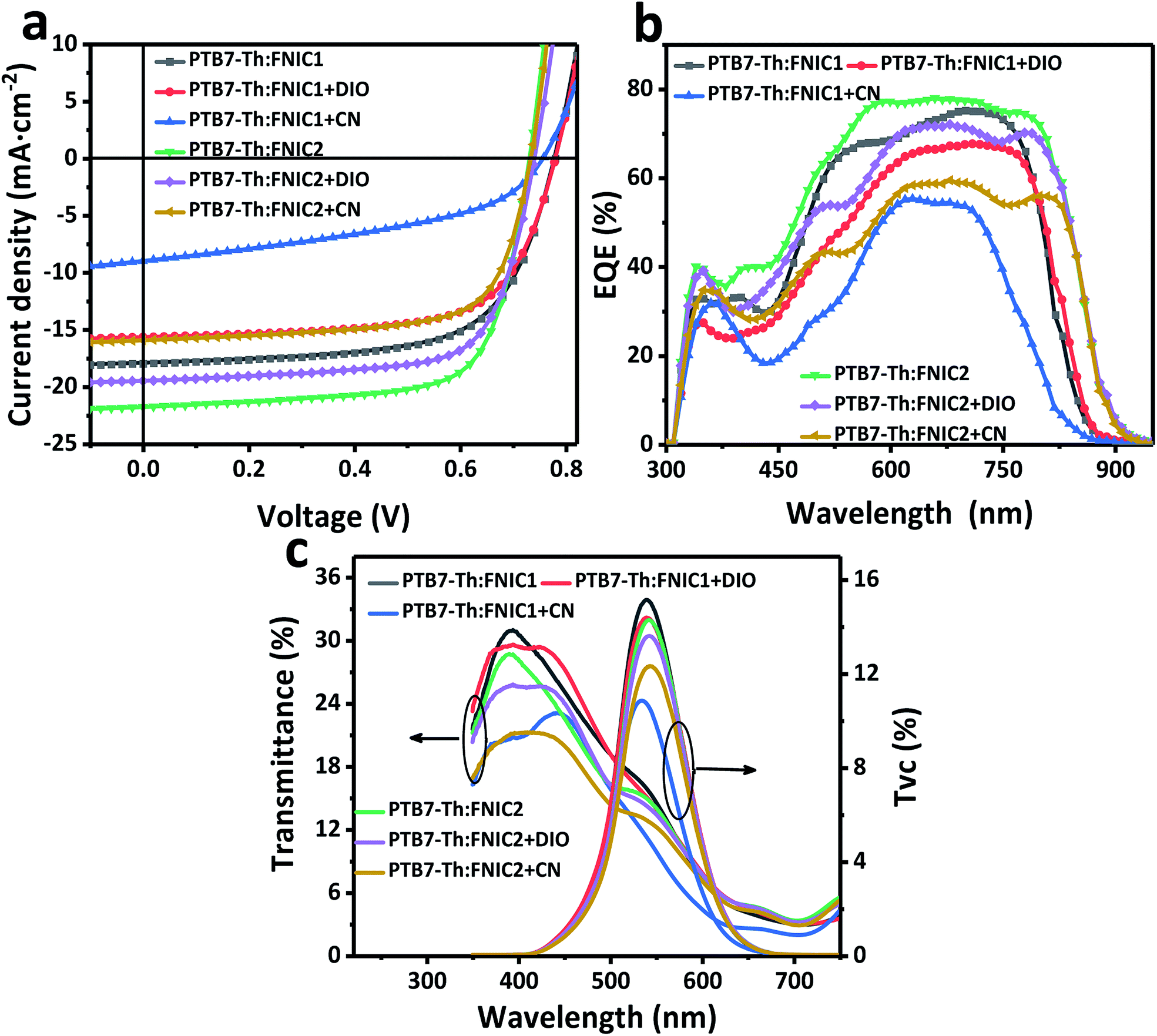 | ||
| Fig. 2 Photovoltaic and transmittance characteristics of PTB7-Th:FNIC1/FNIC2. (a) Current density–voltage curves of semitransparent solar cells based on PTB7-Th:FNIC1 and PTB7-Th:FNIC2, respectively. (b) EQE of semitransparent solar cells based on PTB7-Th:FNIC1 and PTB7-Th:FNIC2, respectively. (c) Optical transmittance and TVS of semitransparent solar cells based on PTB7-Th:FNIC1 and PTB7-Th:FNIC2, respectively. | ||
| Device | Additive | AVTa (%) | V OC (V) | J SC (mA cm−2) | FFb | PCEb (%) |
|---|---|---|---|---|---|---|
a The range of transmissivity is from 350 nm to 750 nm.
b Average values with standard deviation were obtained from 20 devices; the values in parentheses are the parameters of the best devices.
c PTB7-Th:acceptor = 1![[thin space (1/6-em)]](https://www.rsc.org/images/entities/char_2009.gif) :1 (w/w); the area of the device is 4 mm2.
d Device data are from ref. 41. :1 (w/w); the area of the device is 4 mm2.
d Device data are from ref. 41.
|
||||||
| PTB7-Th:FNIC1c | — | 14.7 | 0.769 ± 0.003 (0.772) | 18.27 ± 0.23 (18.33) | 0.634 ± 0.013 (0.646) | 8.91 ± 0.22 (9.14)d |
| DIO | 15.0 | 0.777 ± 0.004 (0.782) | 15.35 ± 0.36 (15.72) | 0.656 ± 0.010 (0.664) | 7.83 ± 0.18 (8.16) | |
| CN | 11.1 | 0.760 ± 0.003 (0.759) | 8.81 ± 0.39 (9.03) | 0.438 ± 0.025 (0.436) | 2.93 ± 0.10 (2.98) | |
| PTB7-Th:FNIC2c | — | 13.9 | 0.727 ± 0.002 (0.728) | 21.42 ± 0.48 (21.87) | 0.716 ± 0.014 (0.726) | 11.1 ± 0.2 (11.6)d |
| DIO | 13.6 | 0.739 ± 0.001 (0.742) | 19.00 ± 0.35 (19.56) | 0.699 ± 0.010 (0.699) | 9.81 ± 0.22 (10.2) | |
| CN | 11.7 | 0.728 ± 0.003 (0.735) | 15.68 ± 0.43 (16.00) | 0.672 ± 0.012 (0.689) | 7.68 ± 0.29 (8.10) | |
Film-depth-dependent crystallinity
Subsequently, we use light absorption spectroscopy to study the influence of the crystallinity of the acceptor in the heterojunction film on the optical transparency and photovoltaic properties. It is noted that X-ray diffraction could be an alternative method to measure crystallinity. However, for lots of organic heterojunction photovoltaic films the X-ray diffraction signals from the π–π stacking (typical distance 3.6–3.9 Å) direction (also charge transport direction) of acceptors are highly overlapped and entangled with those of donors, which makes the calculation of crystalline coherence lengths along the π–π stacking direction for the donor or acceptor rather difficult. Moreover, the diffraction signals of many organic semiconductors along the π–π stacking direction are poor and the X-ray diffraction intensity is not sufficient to warrant a reliable estimation of the film-depth-dependent crystallinity. In particular, for PTB7-Th:acceptor films, currently it is still too difficult to precisely figure out the film crystallinity and film-depth-dependent crystallinity from X-ray diffraction signals. Therefore, in this work we use light absorption spectroscopy to investigate the crystallinity distribution along the vertical film-depth direction.64The variations of optical and electronic properties along the film-depth direction have attracted much attention in recent studies,65–67 and so FLAS has been used for organic photovoltaic cells, photodetectors and field-effect transistors to characterize the film-depth-dependent crystallinity, phase separation, component ratio analysis and so on. These vertical variations of the properties have been used to investigate performance differences among different systems, and can be used to realize better devices. For example, Zhang et al. reported more uniform films of some small molecule:fullerene blends from hot solutions, thus realizing better photovoltaic performances, as compared with the films from cool solutions. FLAS was used to characterize the crystallinity distribution, which shows that better performance is due to the reduction of film-depth-dependent crystallinity variations.68 Lv et al. also performed FLAS for organic photodetector applications, and found that the charge collection efficiency strongly depends on film-depth profiling.69
For the two acceptors, a higher crystallinity induces a red-shift of the 0–0 absorption peaks, and consequently the locations of the absorption peaks in terms of wavelength approximately represent the crystallinity. Moreover, in situ FLAS recently developed by us provides an easily accessible method to obtain the film-depth-dependent distribution of crystallinity.70–72 Actually, FLAS, which can also reveal film-depth-dependent HOMO and LUMO levels of the acceptors because their 0–0 light absorptions are due to excitation from the HOMO to LUMO, directly reveals light absorption and charge transport behaviors and thus could be used to study vertical variations of the optical/electronic properties along the film-depth direction.59 These advantages of FLAS make it a reliable technique to study crystallinity distribution and its roles in vertical optical and photovoltaic properties. The 0–0 excitation absorption peaks of acceptors, extracted upon fitting the blends' absorption profiles using the neat donor and acceptor absorption spectra, are 741 nm (PTB7-Th:FNIC1 + CN), 745 nm (PTB7-Th:FNIC1), 771 nm (PTB7-Th:FNIC1 + DIO), 782 nm (PTB7-Th:FNIC2), 798 nm (PTB7-Th:FNIC2 + DIO) and 811 nm (PTB7-Th:FNIC2 + CN). The red-shift of the 0–0 absorption peaks is due to higher crystalline ordering along the π–π stacking direction of the acceptors. While the absorption profile of PTB7-Th is almost independent on solvent additives, DIO basically shifts the absorption of acceptors towards the infrared region. However, CN decreases the crystallinity of FNIC1 but increases that of FNIC2, as a result of different solvent–acceptor interactions. Fig. 3b shows the dependence of PCE and AVT on the absorption peaks of the acceptors. The less crystalline region of the PTB7-Th:FNIC1 blend and more crystalline region of the PTB7-Th:FNIC2 blend are shown in different parts of the graph. The dependence of JSC, VOC and FF on the absorption peaks of the acceptors also seems to have a similar pattern that increases at first and then decreases with the increase of the absorption peaks of the acceptors, which is shown in Fig. S2.† It is noted that Fig. 3b shows that optimized PCE and AVT are achieved when the absorption peaks of acceptors are around 770–785 nm. Moderate crystallinity leads to a red-shift of the absorption peak of acceptors from the visible region to the infrared region, thus contributing to the improved AVT. Although higher crystallinity further red-shifts the absorption peak of acceptors, the absorption profile is substantially broadened due to the wider distribution of crystallinity which will be discussed later in detail. The broadened absorption profile leads to a higher extinction coefficient even in the visible range and consequently reduces AVT.
 | ||
| Fig. 3 Absorption spectroscopy investigations of PTB7-Th:acceptor films. (a) Normalized light absorption spectra of PTB7-Th:acceptor blends showing the tunable crystallinity. (b) Dependence of PCE and AVT on the 0–0 excitation absorption peaks of the acceptors, the latter of which is extracted from a. The less crystalline region of PTB7-Th:FNIC1 and more crystalline region of PTB7-Th:FNIC2 are shown in different parts of the graph, respectively. The solid lines are a guide to the eye. (c) FLAS spectra of PTB7-Th:FNIC1 films prepared by different solution methods. (d) FLAS spectra of PTB7-Th:FNIC2 films prepared by different solution methods. The dashed lines, as a guideline to eyes, show the fluctuation of absorption peaks as a result of the film-depth-dependent crystallinity distribution. The spectra are vertically shifted for clarity, and each spectrum corresponds to a sub-layer with a thickness of approximately 8–12 nm. The thickness of each sublayer is calculated by fitting the intensity of the absorption spectrum based on the Beer–Lambert law. | ||
To analyze the vertical distribution of the crystallinity, we subsequently perform the film-depth-dependent investigation of the PTB7-Th:acceptor prepared by different solution methods. In situ FLAS (Fig. 3c and d) is conducted via the low-pressure oxygen plasma etching method as reported previously.59 We use oxygen plasma to etch the organic film and in situ monitor the change of absorption spectroscopy. To ensure selective surface etching without damaging the underlying material, the etching process is performed under a relatively low pressure (2–4 Pa). Upon exposure to oxygen plasma, the film's thickness becomes thinner and the absorption spectrum monotonically declines. According to the Beer–Lambert law, we obtain the FLAS spectra via fitting the spectral evolution of the film during etching. As shown in Fig. 3b, PTB7-Th:FNIC1 + DIO and PTB7-Th:FNIC2 exhibit simultaneously optimized PCE and AVT. The film-depth-dependent absorption spectroscopy shows that the acceptor-related absorption peaks are featured with less fluctuation along the film-depth direction, as compared to those for other devices. The film-depth-dependent acceptor-related peak standard deviations of PTB7-Th:FNIC1 + DIO and PTB7-Th:FNIC2 are 29.11 and 26.62, respectively, much less than those of other blends (Fig. 3c and d).
Vertical optical and electronic variations and their impacts on transparency and photovoltaic performance
Because the crystallinity of FNIC2 is generally higher than that of FNIC1 and its light absorption profile is not highly overlapped with that of PTB7-Th, we mainly focus on PTB7-Th:FNIC2 blends to figure out how vertical electronic and optical variations impact the PCE and optical transparency. From the FLAS spectra (Fig. 3d), film-depth-dependent composition profiles are extracted (Fig. 4a) by fitting the absorption spectra of sub-layers in terms of linear overlap of the neat components' spectra. This shows that these three blends are featured with similar vertical phase separation. The donor PTB7-Th is enriched at the top part of the film, close to MoOx in the device, while the acceptor mainly assembles near ZnO. This vertical phase separation formed during solvent evaporation is beneficial for inverted photovoltaic devices.41,70,73 In addition, PTB7-Th:FNIC2 + CN is featured with the most obvious vertical phase separation, and more FNIC2 aggregates near ZnO, as compared with the other two blends. From the FLAS spectra, exciton generation profiles (Fig. 4b) are realized via light interference in combination with the transfer matrix method (the detailed calculation process is shown in the ESI†).74–77 It is noted that the noise-like features are due to the real solar illumination spectra of AM 1.5G. Fig. 5a shows the simulated exciton generation rates G at each film-depth. Although the exciton generation in the near-infrared region is enhanced due to the higher crystallinity of FNIC2, these excitons are mainly located in the vicinity of the ZnO/ITO electrode, inevitably increasing the probability for hole–electron recombination at the electrode surface. Besides this, as the bimolecular recombination in the vicinity of the electrodes is strongly correlated with the spatial distribution of holes and electrons, the holes and electrons dissociated from excitons are more likely to undergo recombination, causing a relatively lower dissociation efficiency, as compared with those with homogeneously distributed excitons in the active layer.78,79 Moreover, this scenario imposes an imbalance for hole and electron transport towards the respective electrodes because the holes need to be transported across the whole film after exciton dissociation while electrons are near the cathode. Consequently, these excitons induced by long wavelength photons do not efficiently contribute to the photocurrent, consistent with the low EQE in this wavelength range as shown in Fig. 2b. From the FLAS spectra (Fig. 3d), film-depth-dependent charge transport levels (the HOMO level of PTB7-Th and LUMO level of the acceptor) can also be extracted (the detailed process is shown in the ESI†). The energy levels of PTB7-Th:FNIC2 + DIO and PTB7-Th:FNIC2 + CN fluctuate more obviously than those of PTB7-Th:FNIC2, which corresponds to the FLAS spectra in Fig. 3d. Using the optical (Fig. 4b) and electronic (Fig. 5b) properties, we simulated charge density–voltage curves with an improved drift-diffusion model. Compared to the traditional model, we take the variation of the HOMO/LUMO caused by film-depth-dependent crystallinity fluctuation into consideration by adding an extra component in the hole/electron current density expression. The expression is (see the detailed information about the numerical simulation in the ESI†). Here, q is the elementary charge, n(p) is the intensity of electrons (holes), μn(p) is the mobility of electrons (holes), kb is the Boltzmann constant, T is the temperature set as 300 K, Fn(p) is the quasi-electric field (QEF) as introduced by Wang et al.24 and Ec(v) is the LOMO (HOMO) energy level of the acceptor (donor). The gradient of the HOMO/LUMO energy level (Ec(v)) contributes to the built-in electric field in the device. w is an adjustment factor to increase the effect of the energy level on the electric field for a more accurate simulation, which is arbitrarily added by us, because the energy levels of localized states could vary discretely from one site to neighboring ones in the active layer, not varying continuously along the film-depth direction. In the model, we treat the fluctuation of the HOMO/LOMO in the active layer as a component of the electric potential, and their gradient performs a trap effect to charge in most cases, which will lead to charge aggregation in a certain site, especially when the fluctuation profile has a deeper wave trough. The simulated photovoltaic performances (Fig. 5c) are in good agreement with the measured ones (Fig. 2a). | (1) |
 | (2) |
 | ||
| Fig. 4 Film-depth-dependent optical investigations of PTB7-Th:FNIC2 prepared from a solution without and with solvent additives (0 nm corresponds to the active layer/MoOx interface). (a) Composition profiles as extracted from FLAS spectra shown in Fig. 3d. (b) Simulated exciton generation profiles (unit, 1025 m−3 s−1 nm−1 at its position and wavelength) from FLAS spectra. The noise-like features are due to the real solar illumination spectra of AM 1.5 G. | ||
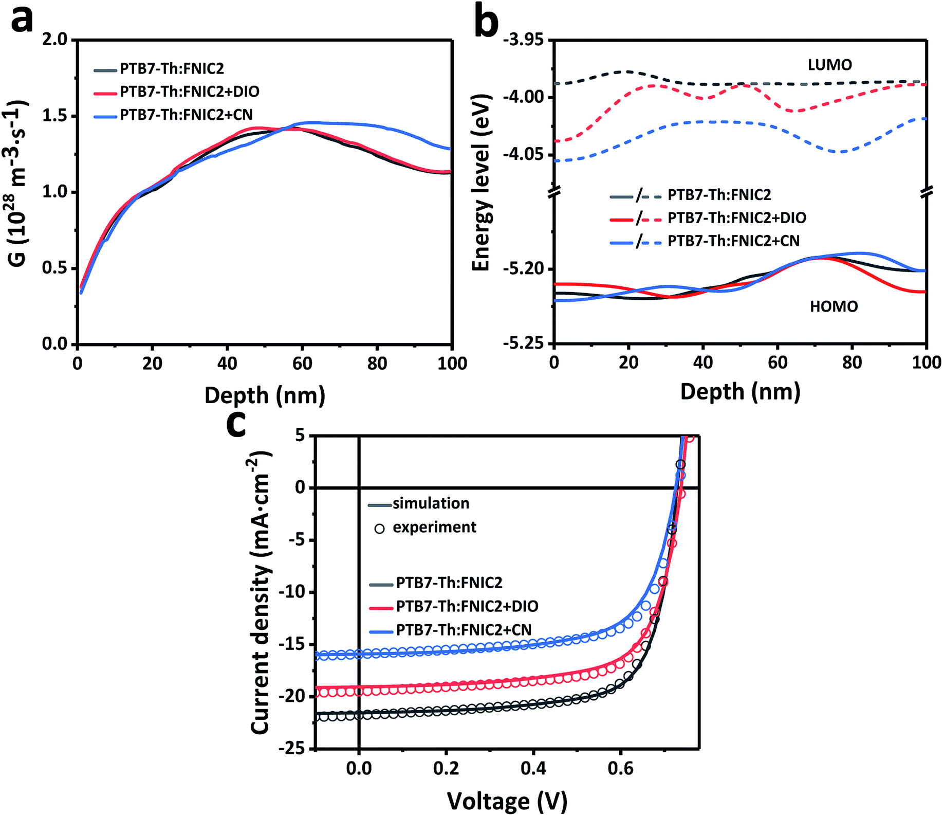 | ||
| Fig. 5 Numerical simulation of PTB7-Th:FNIC2 prepared from a solution without and with solvent additives (0 nm corresponds to the active layer/MoOx interface). (a) Dependence of the simulated exciton generation rate (G) on the film depth. Although exciton generation in the near-infrared region is enhanced due to the higher crystallinity of FNIC2, these excitons are mainly located too close to the ZnO/ITO electrode, and thus do not efficiently contribute to the photocurrent, consistent with the low EQE in this wavelength range as shown in Fig. 2b. (b) Film-depth-dependent charge transport levels (the HOMO level of PTB7-Th and LUMO level of the acceptor) as extracted from the FLAS spectra (Fig. 3d). (c) Simulated charge density–voltage curves from the film-depth-dependent optical (Fig. 4b) and electronic (b) properties. The solid lines are the result of drift-diffusion simulations, and the open circles are experimental results extracted from Fig. 2a. | ||
In principle, the optical variation induced by vertical phase evolution could facilitate photon harvesting at particular film-depths due to the correlation of material variations with light interference within the device. The vertical distribution of transport energy levels, upon avoiding low-energy states (traps) within the semiconductor layers, could promote charge transport to reduce charge recombination. In fact, for many of the solution processed organic bulk heterojunction films, both the donor and acceptor are typically semicrystalline, and due to the long/large molecular chains with side chain steric hindrance the speed of crystallization is relatively slow. Solvent additives change the solvent–material and material–material interactions during film preparation, which significantly influences the phase evolution and crystallization process. The higher crystallinity is usually due to the longer crystallization time, and therefore the ripening process has sufficient time to induce more fluctuation of the crystallinity at different film-depths.
Hereby, we note that the FLAS technique is not suitable for the films for which the domain size is much larger than the film thickness. FLAS relies on oxygen plasma etching, and therefore a large domain size or large roughness will lead to different etching rates of different components, which would make FLAS analysis invalid and unpersuasive.
Conclusions
In summary, in this work two low-bandgap isomeric acceptors in combination with different solution processing methods are used to tune the film-depth-dependent crystallinity of the active layer for semitransparent polymer solar cells. Although certain crystalline stacking of molecules is beneficial for charge transport and optical transparency, it is found that a moderate crystallinity with weak film-depth-dependence contributes to the optimized performance, while a higher crystallinity of acceptors leads to red-shifting of the absorption peak and induces the generation of more excitons in the vicinity of the electrode and could induce additional surface recombination and an imbalance in the transport of holes and electrons. Moreover, large variations of the crystallinity along the film-depth-direction lead to unfavorable variations of the HOMO/LUMO transport levels and inevitably form low energy trap sites, deteriorating the charge transport and increasing recombination. Upon optimizing the film-depth-dependent optical and electronic properties by manipulating the crystallinity and its spatial distribution, a high PCE of 7.6–11.1% with an AVT of 11.7–15.0% and a human-eye TVS up to 12.3–15.2% is realized.Conflicts of interest
There are no conflicts to declare.Acknowledgements
This work was financially supported by the National Natural Science Foundation of China (Grants No. 51873172, 21574103 and 51473132), the China Postdoctoral Science Foundation (Grant No. 2018M643648), the Youth Fund of the State Key Laboratory of Electrical Insulation and Power Equipment (Grant No. EIPE19308), the National Natural Science Foundation of China (51907148), the Natural Science Basic Research Plan in Shaanxi Province of China (2019JQ-070) and the Fundamental Research Funds for the Central Universities (xjh012019023). G. L. thanks the Cyrus Tang Foundation.Notes and references
- L. Lu, T. Zheng, Q. Wu, A. M. Schneider, D. Zhao and L. Yu, Chem. Rev., 2015, 115, 12666–12731 CrossRef CAS PubMed.
- P. Cheng, G. Li, X. Zhan and Y. Yang, Nat. Photonics, 2018, 12, 131–142 CrossRef CAS.
- C. Yan, S. Barlow, Z. Wang, H. Yan, A. K. Y. Jen, S. R. Marder and X. Zhan, Nat. Rev. Mater., 2018, 3, 18003 CrossRef CAS.
- T. Li, S. Dai, Z. Ke, L. Yang, J. Wang, C. Yan, W. Ma and X. Zhan, Adv. Mater., 2018, 30, 1705969 CrossRef PubMed.
- G. Zhang, J. Zhao, P. C. Y. Chow, K. Jiang, J. Zhang, Z. Zhu, J. Zhang, F. Huang and H. Yan, Chem. Rev., 2018, 118, 3447–3507 CrossRef CAS PubMed.
- L. Zhu, W. Zhong, C. Qiu, B. Lyu, Z. Zhou, M. Zhang, J. Song, J. Xu, J. Wang, J. Ali, W. Feng, Z. Shi, X. Gu, L. Ying, Y. Zhang and F. Liu, Adv. Mater., 2019, 31, 1902899 CrossRef CAS PubMed.
- Y. Cui, H. Yao, L. Hong, T. Zhang, Y. Xu, K. Xian, B. Gao, J. Qin, J. Zhang, Z. Wei and J. Hou, Adv. Mater., 2019, 31, 1808356 CrossRef PubMed.
- X. Che, Y. Li, Y. Qu and S. R. Forrest, Nat. Energy, 2018, 3, 422–427 CrossRef CAS.
- L. Meng, Y. Zhang, X. Wan, C. Li, X. Zhang, Y. Wang, X. Ke, Z. Xiao, L. Ding, R. Xia, H.-L. Yip, Y. Cao and Y. Chen, Science, 2018, 361, 1094–1098 CrossRef CAS PubMed.
- J. Yuan, Y. Zhang, L. Zhou, G. Zhang, H.-L. Yip, T.-K. Lau, X. Lu, C. Zhu, H. Peng, P. A. Johnson, M. Leclerc, Y. Cao, J. Ulanski, Y. Li and Y. Zou, Joule, 2019, 3, 1140–1151 CrossRef CAS.
- J. Hou, O. Inganas, R. H. Friend and F. Gao, Nat. Mater., 2018, 17, 119–128 CrossRef CAS PubMed.
- A. M. Leguy, J. M. Frost, A. P. McMahon, V. G. Sakai, W. Kochelmann, C. Law, X. Li, F. Foglia, A. Walsh, B. C. O'Regan, J. Nelson, J. T. Cabral and P. R. Barnes, Nat. Commun., 2015, 6, 7124 CrossRef PubMed.
- Z. Tang, Z. Ma, A. Sanchez-Diaz, S. Ullbrich, Y. Liu, B. Siegmund, A. Mischok, K. Leo, M. Campoy-Quiles, W. Li and K. Vandewal, Adv. Mater., 2017, 29, 1702184 CrossRef PubMed.
- Q. Xue, R. Xia, C. J. Brabec and H.-L. Yip, Energy Environ. Sci., 2018, 11, 1688–1709 RSC.
- P. Cheng, J. Wang, Q. Zhang, W. Huang, J. Zhu, R. Wang, S. Y. Chang, P. Sun, L. Meng, H. Zhao, H. W. Cheng, T. Huang, Y. Liu, C. Wang, C. Zhu, W. You, X. Zhan and Y. Yang, Adv. Mater., 2018, 30, 1801501 CrossRef PubMed.
- P. Shen, M. Yao, J. Liu, Y. Long, W. Guo and L. Shen, J. Mater. Chem. A, 2019, 7, 4102–4109 RSC.
- Y. Xia, X. Xu, L. E. Aguirre and O. Inganäs, J. Mater. Chem. A, 2018, 6, 21186–21192 RSC.
- Y. Cui, C. Yang, H. Yao, J. Zhu, Y. Wang, G. Jia, F. Gao and J. Hou, Adv. Mater., 2017, 29, 1703080 CrossRef.
- B. Dudem, J. W. Jung and J. S. Yu, J. Mater. Chem. A, 2018, 6, 14769–14779 RSC.
- J.-W. Zheng, Q. Sun, C. Gao, J.-D. Chen, W. Li, Y.-X. Zhang, Y. Wang, X. Ling, W. Ma, Y. Li and J.-X. Tang, Org. Electron., 2018, 60, 38–44 CrossRef CAS.
- S. Dai and X. Zhan, Adv. Energy Mater., 2018, 8, 1800002 CrossRef.
- Y. Liu, P. Cheng, T. Li, R. Wang, Y. Li, S. Y. Chang, Y. Zhu, H. W. Cheng, K. H. Wei, X. Zhan, B. Sun and Y. Yang, ACS Nano, 2019, 13, 1071–1077 CAS.
- W. Wang, C. Yan, T. K. Lau, J. Wang, K. Liu, Y. Fan, X. Lu and X. Zhan, Adv. Mater., 2017, 29, 1701308 CrossRef.
- Z. Tang, Z. George, Z. Ma, J. Bergqvist, K. Tvingstedt, K. Vandewal, E. Wang, L. M. Andersson, M. R. Andersson, F. Zhang and O. Inganäs, Adv. Energy Mater., 2012, 2, 1467–1476 CrossRef CAS.
- C. Zhan and J. Yao, Chem. Mater., 2016, 28, 1948–1964 CrossRef CAS.
- Y. Bai, C. Zhao, X. Chen, S. Zhang, S. Zhang, T. Hayat, A. Alsaedi, Z. a. Tan, J. Hou and Y. Li, J. Mater. Chem. A, 2019, 7, 15887–15894 RSC.
- M. He, J. Jung, F. Qiu and Z. Lin, J. Mater. Chem., 2012, 22, 24254–24264 RSC.
- L. Shi, Y. Cui, Y. Gao, W. Wang, Y. Zhang, F. Zhu and Y. Hao, Nanomaterials, 2018, 8, 473 CrossRef PubMed.
- R. Steim, P. Chabrecek, U. Sonderegger, B. Kindle-Hasse, W. Siefert, T. Kroyer, P. Reinecke, T. Lanz, T. Geiger, R. Hany and F. Nüesch, Appl. Phys. Lett., 2015, 106, 193301 CrossRef.
- Y. Kato, M.-C. Jung, M. V. Lee and Y. Qi, Org. Electron., 2014, 15, 721–728 CrossRef CAS.
- M. Hosel, D. Angmo, R. R. Sondergaard, G. A. Dos Reis Benatto, J. E. Carle, M. Jorgensen and F. C. Krebs, Adv. Sci., 2014, 1, 1400002 CrossRef PubMed.
- F. Liu, Z. Zhou, C. Zhang, J. Zhang, Q. Hu, T. Vergote, F. Liu, T. P. Russell and X. Zhu, Adv. Mater., 2017, 29, 1606574 CrossRef PubMed.
- Q. Liu, J. Toudert, T. Li, M. Kramarenko, G. Martínez-Denegri, L. Ciammaruchi, X. Zhan and J. Martorell, Adv. Energy Mater., 2019, 9, 1900463 CrossRef.
- M. Campoy-Quiles, T. Ferenczi, T. Agostinelli, P. G. Etchegoin, Y. Kim, T. D. Anthopoulos, P. N. Stavrinou, D. D. Bradley and J. Nelson, Nat. Mater., 2008, 7, 158–164 CrossRef CAS.
- M. Ghasemi, H. Hu, Z. Peng, J. J. Rech, I. Angunawela, J. H. Carpenter, S. J. Stuard, A. Wadsworth, I. McCulloch, W. You and H. Ade, Joule, 2019, 3, 1328–1348 CrossRef CAS.
- W. Li, J. Cai, Y. Yan, F. Cai, S. Li, R. S. Gurney, D. Liu, J. D. McGettrick, T. M. Watson, Z. Li, A. J. Pearson, D. G. Lidzey, J. Hou and T. Wang, Sol. RRL, 2018, 2, 1800114 CrossRef.
- M. He, M. Wang, C. Lin and Z. Lin, Nanoscale, 2014, 6, 3984–3994 RSC.
- X. Li, X. Du, H. Lin, L. Li, X. Kong, C. Zheng, S. Tao and X. Zhang, Org. Electron., 2018, 62, 195–202 CrossRef CAS.
- L. Ye, H. Hu, M. Ghasemi, T. Wang, B. A. Collins, J. H. Kim, K. Jiang, J. H. Carpenter, H. Li, Z. Li, T. McAfee, J. Zhao, X. Chen, J. L. Y. Lai, T. Ma, J. L. Bredas, H. Yan and H. Ade, Nat. Mater., 2018, 17, 253–260 CrossRef CAS PubMed.
- Z. Zhou, S. Xu, J. Song, Y. Jin, Q. Yue, Y. Qian, F. Liu, F. Zhang and X. Zhu, Nat. Energy, 2018, 3, 952–959 CrossRef CAS.
- J. Wang, J. Zhang, Y. Xiao, T. Xiao, R. Zhu, C. Yan, Y. Fu, G. Lu, X. Lu, S. R. Marder and X. Zhan, J. Am. Chem. Soc., 2018, 140, 9140–9147 CrossRef CAS.
- Y. Lin, F. Zhao, S. K. K. Prasad, J.-D. Chen, W. Cai, Q. Zhang, K. Chen, Y. Wu, W. Ma, F. Gao, J.-X. Tang, C. Wang, W. You, J. M. Hodgkiss and X. Zhan, Adv. Mater., 2018, 30, 1706363 CrossRef PubMed.
- R. Sun, J. Guo, C. Sun, T. Wang, Z. Luo, Z. Zhang, X. Jiao, W. Tang, C. Yang, Y. Li and J. Min, Energy Environ. Sci., 2019, 12, 384–395 RSC.
- Y. Yan, X. Liu and T. Wang, Adv. Mater., 2017, 29, 1601674 CrossRef.
- Y. Zhou, K. L. Gu, X. Gu, T. Kurosawa, H. Yan, Y. Guo, G. I. Koleilat, D. Zhao, M. F. Toney and Z. Bao, Chem. Mater., 2016, 28, 5037–5042 CrossRef CAS.
- C. J. Brabec, M. Heeney, I. McCulloch and J. Nelson, Chem. Soc. Rev., 2011, 40, 1185–1199 RSC.
- Z. Wang, Y. Hu, T. Xiao, Y. Zhu, X. Chen, L. Bu, Y. Zhang, Z. Wei, B. B. Xu and G. Lu, Adv. Opt. Mater., 2019, 7, 1900152 CrossRef.
- S. Bi, Z. Ouyang, S. Shaik and D. Li, Sci. Rep., 2018, 8, 9574 CrossRef PubMed.
- U. Wurfel, D. Neher, A. Spies and S. Albrecht, Nat. Commun., 2015, 6, 6951 CrossRef PubMed.
- B. Liu, R.-Q. Png, J.-K. Tan and P. K. H. Ho, Adv. Energy Mater., 2014, 4, 1200972 CrossRef.
- Y. Xie, F. Yang, Y. Li, M. A. Uddin, P. Bi, B. Fan, Y. Cai, X. Hao, H. Y. Woo, W. Li, F. Liu and Y. Sun, Adv. Mater., 2018, 30, 1803045 CrossRef PubMed.
- T. Liu, L. Huo, S. Chandrabose, K. Chen, G. Han, F. Qi, X. Meng, D. Xie, W. Ma, Y. Yi, J. M. Hodgkiss, F. Liu, J. Wang, C. Yang and Y. Sun, Adv. Mater., 2018, 30, 1707353 CrossRef PubMed.
- S. Albrecht, S. Schäfer, I. Lange, S. Yilmaz, I. Dumsch, S. Allard, U. Scherf, A. Hertwig and D. Neher, Org. Electron., 2012, 13, 615–622 CrossRef CAS.
- P. Cendula, L. Steier, P. A. Losio, M. Grätzel and J. O. Schumacher, Adv. Funct. Mater., 2018, 28, 1702768 CrossRef.
- M. M. Chowdhury and M. K. Alam, Sol. Energy Mater. Sol. Cells, 2015, 132, 107–117 CrossRef CAS.
- B. Y. Finck and B. J. Schwartz, Phys. Rev. Appl., 2015, 4, 034006 CrossRef.
- W. Kaiser, T. Albes and A. Gagliardi, Phys. Chem. Chem. Phys., 2018, 20, 8897–8908 RSC.
- R. C. I. MacKenzie, T. Kirchartz, G. F. A. Dibb and J. Nelson, J. Phys. Chem. C, 2011, 115, 9806–9813 CrossRef CAS.
- L. Bu, S. Gao, W. Wang, L. Zhou, S. Feng, X. Chen, D. Yu, S. Li and G. Lu, Adv. Electron. Mater., 2016, 2, 1600359 CrossRef.
- G. F. Burkhard, E. T. Hoke and M. D. McGehee, Adv. Mater., 2010, 22, 3293–3297 CrossRef CAS PubMed.
- G. Han, Y. Guo, X. Song, Y. Wang and Y. Yi, J. Mater. Chem. C, 2017, 5, 4852–4857 RSC.
- Q. Liu, J. Toudert, F. Liu, P. Mantilla-Perez, M. M. Bajo, T. P. Russell and J. Martorell, Adv. Energy Mater., 2017, 7, 1701201 CrossRef.
- O. K. Kwon, M. A. Uddin, J. H. Park, S. K. Park, T. L. Nguyen, H. Y. Woo and S. Y. Park, Adv. Mater., 2016, 28, 910–916 CrossRef CAS PubMed.
- Y. Wang, Y. Zhang, G. Lu, X. Feng, T. Xiao, J. Xie, X. Liu, J. Ji, Z. Wei and L. Bu, ACS Appl. Mater. Interfaces, 2018, 10, 13741–13747 CrossRef CAS PubMed.
- J. Zhang, M. H. Futscher, V. Lami, F. U. Kosasih, C. Cho, Q. Gu, A. Sadhanala, A. J. Pearson, B. Kan, G. Divitini, X. Wan, D. Credgington, N. C. Greenham, Y. Chen, C. Ducati, B. Ehrler, Y. Vaynzof, R. H. Friend and A. A. Bakulin, Adv. Energy Mater., 2019, 1902145 CrossRef.
- L. Bu, Y. Qiu, P. Wei, L. Zhou, W. Lu, S. Li and G. Lu, Phys. Rev. Appl., 2016, 6, 054022 CrossRef.
- Y. Hu, P. Wei, X. Wang, L. Bu and G. Lu, Phys. Rev. Appl., 2018, 10, 054024 CrossRef CAS.
- Y. Zhang, D. Deng, Z. Wang, Y. Wang, J. Zhang, J. Fang, Y. Yang, G. Lu, W. Ma and Z. Wei, Adv. Energy Mater., 2017, 7, 1701548 CrossRef.
- L. Lv, J. Yu, X. Sui, J. Wu, X. Dong, G. Lu, X. Liu, A. Peng and H. Huang, J. Mater. Chem. C, 2019, 7, 5739–5747 RSC.
- P. Bi, T. Xiao, X. Yang, M. Niu, Z. Wen, K. Zhang, W. Qin, S. K. So, G. Lu, X. Hao and H. Liu, Nano Energy, 2018, 46, 81–90 CrossRef CAS.
- Q. Liang, X. Jiao, Y. Yan, Z. Xie, G. Lu, J. Liu and Y. Han, Adv. Funct. Mater., 2019, 29, 1807591 CrossRef CAS.
- Y. Zhao, G. Wang, Y. Wang, T. Xiao, M. A. Adil, G. Lu, J. Zhang and Z. Wei, Sol. RRL, 2019, 3, 1800333 CrossRef.
- J. Fang, D. Deng, Z. Wang, M. A. Adil, T. Xiao, Y. Wang, G. Lu, Y. Zhang, J. Zhang, W. Ma and Z. Wei, ACS Appl. Mater. Interfaces, 2018, 10, 12913–12920 CrossRef CAS PubMed.
- L. A. A. Pettersson, L. S. Roman and O. Inganäs, J. Appl. Phys., 1999, 86, 487–496 CrossRef CAS.
- X. Zhao, B. Mi, Z. Gao and W. Huang, Sci. China: Phys., Mech. Astron., 2011, 54, 375–387 CAS.
- C. Ahläng, O. J. Sandberg and R. Österbacka, Phys. Rev. B, 2018, 98, 075306 CrossRef.
- T. M. Burke, S. Sweetnam, K. Vandewal and M. D. McGehee, Adv. Energy Mater., 2015, 5, 1500123 CrossRef.
- O. J. Sandberg, S. Sanden, A. Sundqvist, J. H. Smatt and R. Osterbacka, Phys. Rev. Lett., 2017, 118, 076601 CrossRef.
- A. Melianas, F. Etzold, T. J. Savenije, F. Laquai, O. Inganas and M. Kemerink, Nat. Commun., 2015, 6, 8778 CrossRef CAS.
Footnote |
| † Electronic supplementary information (ESI) available. See DOI: 10.1039/c9ta11613c |
| This journal is © The Royal Society of Chemistry 2020 |