DOI:
10.1039/D0SC04047A
(Edge Article)
Chem. Sci., 2020,
11, 11601-11612
Boron(III) β-diketonate-based small molecules for functional non-fullerene polymer solar cells and organic resistive memory devices†
Received
24th July 2020
, Accepted 17th September 2020
First published on 8th October 2020
Abstract
A class of acceptor–donor–acceptor chromophoric small-molecule non-fullerene acceptors, 1–4, with difluoroboron(III) β-diketonate (BF2bdk) as the electron-accepting moiety has been developed. Through the variation of the central donor unit and the modification on the peripheral substituents of the terminal BF2bdk acceptor unit, their photophysical and electrochemical properties have been systematically studied. Taking advantage of their low-lying lowest unoccupied molecular orbital energy levels (from −3.65 to −3.72 eV) and relatively high electron mobility (7.49 × 10⁻⁴ cm2 V−1 s−1), these BF2bdk-based compounds have been employed as non-fullerene acceptors in organic solar cells with maximum power conversion efficiencies of up to 4.31%. Moreover, bistable resistive memory characteristics with charge-trapping mechanisms have been demonstrated in these BF2bdk-based compounds. This work not only demonstrates for the first time the use of a boron(III) β-diketonate unit in constructing non-fullerene acceptors, but also provides more insights into designing organic materials with multi-functional properties.
Introduction
Due to their favorable properties including light weight, mechanical flexibility and cost-effectiveness, solution-processable bulk-heterojunction (BHJ) organic solar cells (OSCs) have received enormous attention in the past two decades.1–3 Most of the high-performance OSCs reported so far are made from fullerene derivatives as the acceptor materials.4,5 However, the intrinsic drawbacks of fullerene derivatives, such as challenging purification process, low absorptivity in the deep-red region and morphological instability, limit the commercial interest for practical applications.6,7 Non-fullerene acceptors (NFAs), especially molecular NFAs with well-defined structures, have become more attractive as compared to the fullerenes. Particularly, the electronic absorption molar absorptivity, the highest occupied molecular orbital (HOMO) and the lowest unoccupied molecular orbital (LUMO) energy levels and charge carrier transport properties of the NFAs can be facilely tuned by structural modifications.7,8
In recent years, the development of NFAs has boosted the power conversion efficiencies (PCEs) of NFA-based OSCs, making them comparable or even superior to those of their fullerene-based counterparts.9 From the molecular design point of view, the introduction of electron-donating and electron-accepting chromophores is the key strategy for constructing a charge-transfer-type NFA molecule, which could readily yield the resultant molecule with high charge carrier mobilities and extend its absorption profile into the deep-red region.10,11 Among all electron-accepting chromophores, boron(III)-containing moieties are anticipated to be promising candidates due to the vacant p-orbital on the boron center, making them inherently electron deficient.12–14 To date, a number of molecular NFAs using three-coordinate boranes or four-coordinate borates as electron-accepting chromophores for solution-processable OSCs have been reported in the literature;15–22 however, only those NFAs containing double B ← N bridged bipyridine-based four-coordinate borates show PCEs exceeding 4%.21,22
On the other hand, air-stable boron(III) β-diketonates, a family of classical four-coordinate borates, have proven to show strong luminescence, large extinction coefficients and nonlinear optical properties.23 Notably, they have been extensively applied in materials science and bioimaging in the past decades.23 The rich photophysical properties of boron(III) β-diketonate moieties also make them an attractive organic π-system in the construction of functional materials for various optoelectronic applications.24–32 For instance, Ono and coworkers demonstrated that the integration of difluoroboron(III) β-diketonates into oligothiophene skeletons endowed the compounds with high electron mobilities in an order of 10−3 cm2 V−1 s−1 in organic field-effect transistors (OFETs).27 Taking advantage of the strong electron-withdrawing ability of the acetylacetonate boron(III) difluoride unit, Adachi and coworkers were able to prepare a high-performance near-infrared (NIR) thermally activated delayed fluorescence (TADF) emitter based on a boron(III) difluoride-chelated curcuminoid dye for application in organic light-emitting diodes (OLEDs).29 Additionally, our group successfully designed and synthesized a class of boron(III) β-diketonate functionalized photochromic dithienylethenes with interesting NIR photochromic behavior and donor–acceptor small molecules with distinct conductance switching behavior, showing great potential for optical and electronic memory storage applications.31–34 Despite the promise of this class of compounds in various potential applications, none of the reports were found to involve the incorporation of boron(III) β-diketonate into NFAs for OSCs. In light of the aforementioned scenarios, it is envisaged that the incorporation of the boron(III) β-diketonate core in NFAs can yield NIR-absorbing materials, which could capture more light for photocurrent generation, and hence improve the PCE. With our continuous interest in the development of new organoboron-based functional materials,31–38 herein we report the design and synthesis of a class of acceptor–donor–acceptor (A–D–A) type NFAs containing difluoroboron(III) β-diketonate (BF2bdk) moieties as acceptor units, i.e.1–4, and their molecular structures are depicted in Fig. 1. The BF2 moiety is particularly chosen for enhancing the electron-accepting properties, as well as minimizing the steric bulkiness of the BF2bdk moiety and thus planarizing the molecular framework, all of which are anticipated to be promising to achieve excellent electron-transport properties. Noticeably, solution-processable BHJ OSCs using two dimensional (2D)-conjugated bithienyl-benzodithiophene-alt-fluorobenzotriazole copolymers (J61 and J52, Fig. 1) as the donor materials and 1–4 as the acceptor materials exhibit satisfactory PCEs of up to 4.31%, demonstrating for the first time the potential of the BF2bdk moiety for constructing NFAs. In addition, the versatility of these BF2bdk end-capped compounds in the fabrication of organic resistive memory devices has been demonstrated and the corresponding conductance switching mechanism has also been explored.
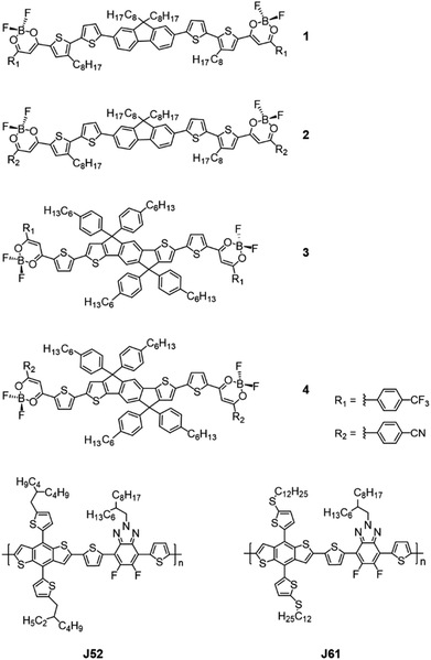 |
| | Fig. 1 Chemical structures of 1–4, J52 and J61. | |
Results and discussion
Synthesis and characterization
All the trimethylstannyl precursors were synthesized according to literature procedures,39,40 and were subsequently reacted with the corresponding 1-(5-bromo-4-octylthiophen-2-yl)ethan-1-one and 1-(5-bromothiophen-2-yl)ethan-1-one41via Stille cross-coupling reactions to afford diacetyl substituted intermediates Flu-(Th-oct-Th-COMe)2 and IDT-(Th-COMe)2, respectively. The target compounds 1–4 were then prepared via Claisen condensation reactions of Flu-(Th-oct-Th-COMe)2 and IDT-(Th-COMe)2 with the corresponding methyl 4-(trifluoromethyl)benzoate and methyl 4-cyanobenzoate, followed by the coordination with BF3·OEt2. The synthetic routes of 1–4 are provided in the ESI.† All the reaction intermediates and the target compounds 1–4 were characterized by 1H NMR spectroscopy, high resolution electron ionization (EI) or electrospray ionization (ESI) mass spectroscopy. Target compounds 1–4 were also confirmed by 19F{1H} and 11B{1H} NMR spectroscopy and elemental analyses. Compound 1 was structurally characterized by single-crystal X-ray crystallographic analysis (Fig. 2 and S1, and Tables S1 and S2†). All the compounds 1–4 show good solubilities in common organic solvents, such as dichloromethane, chloroform and chlorobenzene, which is favorable for fabricating solution-processable electronic devices. The thermal properties of 1–4 were investigated by thermogravimetric analysis (TGA) and differential scanning calorimetry (DSC). TGA data demonstrate that 1–4 exhibit good thermal stabilities with decomposition temperatures of ≥309 °C (Fig. S2 and Table S3†). According to the DSC curves (Fig. S3†), no obvious thermal transitions are observed for 1–4 below 230 °C, indicative of the amorphous nature of these compounds in the solid state.42,43 This is also supported by preliminary 2D-GIWAXS experiments, which do not show well-defined diffraction signals.
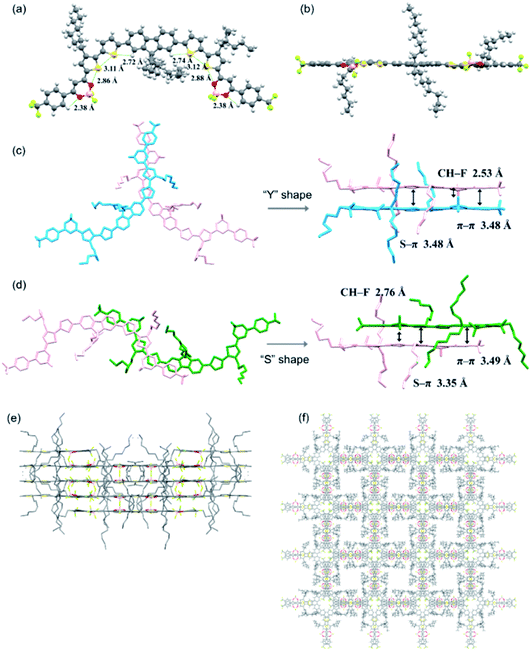 |
| | Fig. 2 (a) Top and (b) side views of the crystal structure of compound 1. (c) “Y” and (d) “S” shape J-aggregations with selected interaction distances. Here the molecules of different layers are shown in different colors for clarity. (e) Molecular layer-by-layer packing diagram and (f) 3D interpenetrating network of compound 1. | |
X-ray crystal structure studies
Solid state packing of organic semiconductors has been demonstrated to have significant impacts on the electronic coupling interactions and thus the charge transport properties.44,45 Therefore, efforts were made to grow single crystals of these BF2bdk end-capped compounds. X-ray-quality crystals of compound 1 were successfully obtained from a concentrated chlorobenzene solution via slow solvent evaporation at room temperature. As shown in Fig. 2a and Table S1,† multiple conformational locks caused by intramolecular noncovalent C–H⋯S (2.721 and 2.745 Å), S⋯S (3.111 and 3.117 Å), S⋯O (2.858 and 2.879 Å) and C–H⋯O (2.376 and 2.378 Å) interactions are revealed, which endow the molecule with high planarity, with small torsion angles (2.71–10.89°) between adjacent aromatic rings (Fig. 2b). Such a highly coplanar backbone is beneficial to promote π-conjugation and electron delocalization, leading to enhanced light-harvesting and charge carrier transport.46 Particularly, small torsion angles of 2.71–5.93° and 5.50–7.62° between the dioxaborine rings and their adjacent thiophene and phenyl rings, respectively, as well as the small size of the fluorine atoms on the boron centers are anticipated to favor the formation of intermolecular π–π stacking interactions between the terminal BF2bdk-based acceptor moieties, which have been demonstrated to facilitate electron transport in A–D–A type NFAs.47,48 Meanwhile, the octyl chains on the central fluorene moiety and the thiophene rings are oriented perpendicular to the π-conjugated backbone, which could help to increase the solubility required for solution processing and alleviate overly large domain aggregate formation to achieve a reasonably small domain size in the corresponding blend film.46 Interestingly, two types of J-aggregations dominated by π–π interactions between the intermolecular terminal BF2bdk-based acceptor moieties are found in the crystal packing (Fig. 2c and d). Specifically, the intermolecular C–H⋯F interaction (2.53 Å) and the intermolecular S⋯π interaction between dioxaborine rings (3.48 Å) lead to the formation of “Y” shape J-aggregates with a π–π stacking distance of 3.48 Å (Fig. 2c). Besides, intermolecular interactions involving C–H⋯F and S⋯π contacts also lead to the formation of “S” shape J-aggregation with a π–π stacking distance of around 3.49 Å, which would be favorable for long distance charge transport (Fig. 2d).49 The π–π interactions together with other intermolecular interactions, such as C⋯F, C–H⋯F, C–H⋯S, and C–H⋯O interactions (Table S1†), enable the molecules to undergo self-assembly into a layer-by-layer packing (Fig. 2e) and eventually a three-dimensional (3D) interpenetrating network (Fig. 2f), in which isotropic electron transport could be envisaged.49–51 The single crystal structure of compound 1 and its packing not only suggest the favorable packing motif for the potential application of the BF2bdk-based acceptor moiety in constructing A–D–A type NFAs, but also provide for the first time molecular geometry insights into A–D–A type NFAs with a central tricyclic donor moiety.
Optical and electrochemical properties
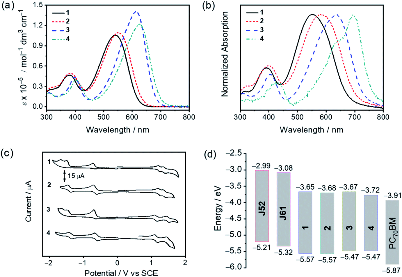
In dichloromethane solution, the electronic absorption spectra of 1–4 generally show similar characteristics, featuring strong absorptions in the range of 500–700 nm with molar extinction coefficients (ε) in the order of 105 dm3 mol−1 cm−1. The electronic absorption spectra of 1–4 in dilute dichloromethane solution and the normalized electronic absorption spectra of 1–4 in pristine thin films at 298 K are shown in Fig. 3a and b, respectively. The corresponding UV-vis absorption spectral data are summarized in Table 1. Changing the peripheral substituents from trifluoromethyl groups in 1 and 3 to cyano groups in 2 and 4 has led to a red shift in the absorption maxima from 539 nm for 1 to 552 nm for 2 and from 615 nm for 3 to 628 nm for 4, respectively, due to the enhanced intramolecular charge transfer (ICT) character induced by the more electron-accepting cyano groups. On the other hand, by employing the indacenodithiophene (IDT) moiety instead of the fluorene moiety as the donor unit, a remarkable red shift by ca. 2200 cm−1 was observed from 1 to 3 as well as from 2 to 4. In the pristine thin film, the absorption maxima of 1–4 were further red-shifted by 470–1535 cm−1, which can be attributed to the existence of intermolecular interactions in the thin film state. It is noteworthy that an intense shoulder at 695 nm is observed in the thin film absorption spectrum of 4, which could be indicative of a high degree of molecular ordering in the solid state.52 The corresponding optical bandgaps (Eoptg, defined as 1240/λonset) of 1–4 are estimated to be 1.82, 1.74, 1.69 and 1.59 eV, respectively. Meanwhile, as shown in Fig. 3b and S4,† the pristine thin film absorption profiles of 3 and 4, when compared with those of 1 and 2, are found to be more complementary to those of polymeric donors J61 and J52 (Fig. 1), which is beneficial to the enhancement of light-harvesting. In addition, the trends in their electronic absorption behaviors are further supported by time-dependent density functional theory (TDDFT) calculations (see the ESI†).
 |
| | Fig. 3 (a) Electronic absorption spectra of 1–4 in dichloromethane solution. (b) Normalized electronic absorption spectra of the thermally annealed pristine thin films of 1–4 spin-coated from their chlorobenzene solutions. (c) Cyclic voltammograms of 1–4 in dichloromethane solution (0.1 M nBu4NPF6) according to IUPAC conventions. (d) Energy level diagram showing the alignment of J52, J61, 1–4 and PC70BM. | |
Table 1 Optical and electrochemical data of 1–4
| Compound |
λ
solmax
/nm (εmax/dm3 mol−1 cm−1) |
λ
filmmax
/nm |
E
optg
/eV |
HOMOd/eV |
LUMOe/eV |
E
cvg
/eV |
|
Absorption maximum of the lowest energy absorption band measured in dichloromethane solution (10−5 M).
Absorption maximum of the lowest energy absorption band measured in pristine thin film.
Determined from the onset of absorption band of the thin film.
E
HOMO = −[Eox1/2 (vs. Fc+/Fc) + 4.80] eV.
E
LUMO = −[Ered1/2 (vs. Fc+/Fc) + 4.80] eV.
E
cvg = EHOMO − ELUMO. E°(Fc+/Fc) = +0.46 V vs. SCE in dichloromethane (0.1 M nBu4NPF6).
|
|
1
|
539 (105![[thin space (1/6-em)]](https://www.rsc.org/images/entities/char_2009.gif) 360) 360) |
553 |
1.82 |
−5.57 |
−3.65 |
1.92 |
|
2
|
552 (109440) |
580 |
1.74 |
−5.57 |
−3.68 |
1.89 |
|
3
|
615 (140860) |
638 |
1.69 |
−5.47 |
−3.67 |
1.80 |
|
4
|
628 (121180) |
695 |
1.59 |
−5.47 |
−3.72 |
1.75 |
To investigate the electrochemical properties of 1–4, cyclic voltammetry (CV) was carried out in dichloromethane solution (0.1 M nBu4NPF6) at room temperature. Generally, all compounds exhibit two quasi-reversible oxidation couples with potentials from +1.13 V to +1.48 V vs. saturated calomel electrode (SCE), which can be attributed to the successive one-electron oxidation of the donor units. For the reduction, 1 and 3 with trifluoromethyl-substituted difluoroboron(III) diketonates show one quasi-reversible reduction couple and two irreversible reduction waves, while 2 and 4 with cyano-substituted difluoroboron(III) diketonates show two quasi-reversible reduction couples, respectively. The first quasi-reversible reduction couple of 1–4 is assigned to the one-electron reduction of their respective difluoroboron diketonate. The cyclic voltammograms of 1–4 are depicted in Fig. 3c, and the corresponding electrochemical data are tabulated in Tables 1 and S4.† The HOMO and LUMO energy levels, which are estimated from the first redox potentials for oxidation and reduction, are found to be at ca. −5.57 to −5.47 eV and at ca. −3.72 to −3.65 eV, respectively. It is found that the HOMO energy levels are sensitive to the central donor moiety, while the LUMO energy levels can be affected by both the terminal acceptor and central donor moieties. Particularly, the LUMO levels of 1–4 are lower-lying than those of J61 (−3.08 eV) and J52 (−2.99 eV),53 which allows them to serve as promising electron acceptors with these polymers in OSCs. Meanwhile, the LUMO levels of 1–4 are higher-lying than that of the fullerene acceptor PC70BM (−3.91 eV),54 which is favorable for achieving a high open circuit voltage (Voc). The energy level diagram showing the alignment of J52, J61, 1–4 and PC70BM is shown in Fig. 3d. The trend in their electrochemical behavior is consistent with that of their optical properties and is further supported by density functional theory (DFT) calculations (see the ESI†).
Photovoltaic properties
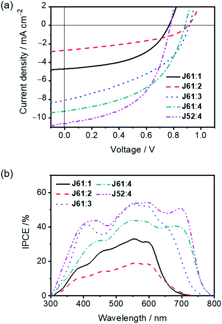
To explore the potential of 1–4 as electron acceptors for photovoltaic applications, thermally annealed OSCs with an inverted structure were fabricated using J61 and J52 as the photovoltaic donor materials.53 The current density–voltage (J–V) characteristics are depicted in Fig. 4a and S5a,† and the corresponding photovoltaic parameters are summarized in Tables 2 and S5.† Comparing 1 and 2, which have the same central fluorene moiety, the device fabricated with the J61:1 blend exhibits a higher PCE of 1.49% with a Voc of 0.77 V, a short-circuit current density (Jsc) of 4.10 mA cm−2 and a fill factor (FF) of 0.47. The better performance of the device fabricated with the J61:1 blend can be primarily ascribed to its higher Jsc. Interestingly, the Voc of the device fabricated with the J61:2 blend is approximately 140 mV higher than that with the J61:1 blend although 2 shows a lower-lying LUMO energy level than that of 1. This result can be explained by the studies of charge carrier recombination dynamics (vide infra), in which a longer charge carrier lifetime under the working conditions for the device fabricated with the J61:2 blend is revealed. On the other hand, by employing IDT as the central donor moiety, devices fabricated with the J61:3 and J61:4 blends generally show significantly higher Jsc as compared to those with the J61:1 and J61:2 blends, which could be ascribed to the more complementary absorption between the IDT-centered small molecules (i.e.3 and 4) and J61 (Fig. S4†). Particularly, the device fabricated with the J61:4 blend achieves the best performance, in which a PCE of 4.06% with a Voc of 0.89 V, a Jsc of 9.27 mA cm−2 and a FF of 0.50 is obtained. The much higher Jsc and the slightly lower Voc of the device fabricated with the J61:4 blend are in good agreement with the broader absorption band and lower-lying LUMO energy level of 4, respectively, when compared with those of 3. Moreover, devices fabricated with J52:1–4 also show moderate photovoltaic performances (Tables 2 and S5†). Notably, by using J52 instead of J61 as the donor material, the PCE of the device fabricated with the J52:4 blend was boosted to 4.31% with a simultaneously improved Jsc of 10.58 mA cm−2 and FF of 0.52. For comparison, the as-cast device fabricated with the J52:4 blend was also fabricated, in which a relatively lower Jsc of 6.52 mA cm−2 and thus a lower PCE of 2.90% are obtained.
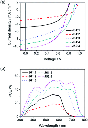 |
| | Fig. 4 (a) J–V characteristics and (b) IPCE spectra of devices fabricated with the J61:1–4 and J52:4 blends (1:1, w/w; thermal annealing at 110 °C for 10 min; under the illumination of AM1.5G, 100 mW cm−2). | |
Table 2 Photovoltaic parameters of devices using 1–4 as acceptor materials under the illumination of AM1.5G, 100 mW cm−2
| Active layera |
J
sc/mA cm−2 |
V
oc/V |
FF |
PCE/% |
|
Thermal annealing at 110 °C for 10 min; average values and deviations in parentheses, calculated from 10 devices.
|
|
J61:1 |
4.10 (4.05 ± 0.05) |
0.77 (0.76 ± 0.01) |
0.47 (0.43 ± 0.03) |
1.49 (1.35 ± 0.13) |
|
J61:2 |
2.99 (2.90 ± 0.09) |
0.91 (0.91 ± 0.01) |
0.46 (0.42 ± 0.04) |
1.29 (1.14 ± 0.15) |
|
J61:3 |
8.09 (8.02 ± 0.06) |
0.92 (0.92 ± 0.01) |
0.43 (0.40 ± 0.03) |
3.17 (3.02 ± 0.14) |
|
J61:4 |
9.27 (9.10 ± 0.15) |
0.89 (0.88 ± 0.01) |
0.50 (0.45 ± 0.04) |
4.06 (3.90 ± 0.16) |
|
J52:4 |
10.58 (10.45 ± 0.12) |
0.78 (0.78 ± 0.01) |
0.52 (0.47 ± 0.05) |
4.31 (4.16 ± 0.14) |
In addition, devices made with the J61:1 and J61:2 blends show the incident photon-to-current efficiency (IPCE) in the range of 300–750 nm with maximum IPCEs of 33% at 560 nm and 19% at 560 nm, respectively (Fig. 4b). The pronounced improvement in the IPCE for the device made with the J61:1 blend is in good agreement with the corresponding Jsc value and suggests the occurrence of higher exciton dissociation efficiency.55 Broader and more intense IPCEs are obtained for devices fabricated with the J61:3 and J61:4 blends, in which maximum IPCEs of 53% at 560 nm and 44% at 550 nm could be achieved, respectively. By replacing J61 with J52 as the donor material in the devices based on 4, the photovoltaic response can be further enhanced, in which much higher IPCEs, especially in the range of 600–800 nm, are achieved. All these observations in the IPCE spectra are in good agreement with the absorption profiles of the corresponding thermally annealed blend films (Fig. S4b†) and are in line with the trend of the Jsc values measured from J–V curves (Fig. 4b).
Charge carrier mobility studies
To get a better understanding of the impact of charge transport properties on the photovoltaic responses, the hole (μh) and electron mobilities (μe) of thermally annealed J61:1–4 and J52:4 blend films were measured using the space-charge-limited current (SCLC) method from the hole-only and electron-only devices, respectively (see the ESI† for details).56 Generally, μh and μe of all the blend films are determined to be in the range of 1.27–4.37 × 10⁻⁴ cm2 V−1 s−1 and 1.41–7.49 × 10⁻⁴ cm2 V−1 s−1, respectively, suggesting efficient charge transport in the domain of donor (J61 and J52) and acceptor materials (1–4) (Fig. S6† and Table 3). Particularly, the μe values are comparable to those of the structurally related efficient electron acceptors for OSCs.57,58 Compared to J61:1 and J61:2 blend films, J61:3 and J61:4 blend films exhibit higher μe, which could be ascribed to the more rigid and extended π-conjugation of the IDT-based backbone than the fluorene-based backbone58,59 as well as smaller dipole moments of 3 (0.88 D) and 4 (0.84 D) when compared to those of 1 (15.45 D) and 2 (12.70 D), as revealed by DFT calculations. Similar observations have also been made in other systems, where a smaller dipole moment can avoid a large energetic disorder and thus facilitate charge-carrier transport of donor–acceptor type materials in the solid state.60–63 Moreover, the qualitative photoluminescence (PL) quenching studies show that the PL intensities of J61, J52 and 1–4 are severely quenched in the thermally annealed blend films upon excitation at the corresponding absorption maximum of the pristine thin films, respectively (for details see ESI Fig. S7 and S8, and Table S6†). Specifically, the μh and μe for the J61:3 and J61:4 blends are found to be almost two and five times higher than those for the J61:1 and J61:2 blend films, respectively. These increased charge carrier mobilities support the higher Jsc for the devices fabricated with the J61:3 and J61:4 blends.55,64 It is also noted that the device based on the J61:3 blend exhibits the lowest FF, which can be attributed to a relatively unbalanced μh/μe ratio of 0.34. By replacing J61 with J52, more balanced charge carrier mobilities with a μh/μe ratio of 1.08 have been achieved for the J52:4 blend. This may explain the slightly higher Jsc and FF for the device based on the J52:4 blend when compared with those based on the J61:4 blend.64,65
Table 3 Hole and electron mobilities of devices fabricated with the J61:1–4 and J52:4 blends
| Active layera |
μ
h/cm2 V−1 s−1 |
μ
e/cm2 V−1 s−1 |
μ
h/μe ratio |
|
Thermal annealing at 110 °C for 10 min.
|
|
J61:1 |
1.83 × 10⁻⁴ |
1.41 × 10⁻⁴ |
1.30 |
|
J61:2 |
1.27 × 10⁻⁴ |
1.62 × 10⁻⁴ |
0.78 |
|
J61:3 |
2.73 × 10⁻⁴ |
7.49 × 10⁻⁴ |
0.34 |
|
J61:4 |
2.99 × 10⁻⁴ |
6.39 × 10⁻⁴ |
0.47 |
|
J52:4 |
4.37 × 10⁻⁴ |
4.06 × 10⁻⁴ |
1.08 |
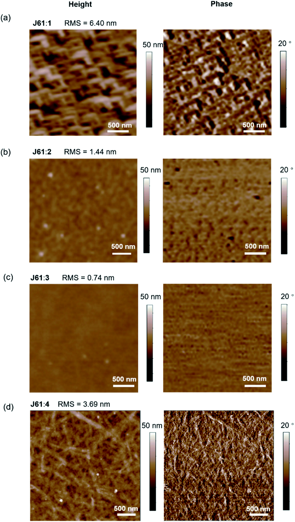
Morphology studies
The surface morphologies of thermally annealed J61:1–4 and J52:4 blend films were investigated on quartz substrates by tapping mode atomic force microscopy (AFM). As shown in the height images (Fig. 5), all the J61-based blend films show uniform surface morphologies, with root-mean-square (RMS) roughnesses of 6.40 nm, 1.44 nm, 0.74 nm and 3.69 nm for the J61:1–4 blend films, respectively. Comparing the J61:1 and J61:2 blend films, the larger RMS of the J61:1 blend film reveals the presence of a pronounced phase separation with enhanced domain purity, which is advantageous for charge transport.66–68 These findings are in good agreement with the higher Jsc and FF in the corresponding OSC devices. Similar results are also observed for the OSC devices fabricated with the J61:4 blend when compared to those fabricated with the J61:3 blend. Surprisingly, a slightly decreased RMS of 2.66 nm along with fine-grained texture is observed in the J52:4 blend film, which is beneficial for exciton dissociation and charge carrier generation, probably explaining the improved Jsc and FF in the device fabricated with J52:4 as compared with those with J61:4 (Fig. 5 and S9†).68–70 For comparison, the surface morphology of the as-cast J52:4 blend film was also studied, in which a rather large RMS of 11.11 nm with excessive phase separation is observed (Fig. S9†). This indicates that the thermal annealing treatment can improve the miscibility between the donor and acceptor materials in the blend, which could explain the much higher Jsc and PCE of the corresponding thermally annealed J52:4-based OSC device as compared to those of the as-cast device. These results reveal that appropriate manipulation of the surface morphology is highly important to balance and optimize the resultant exciton dissociation and charge transport in the blend.
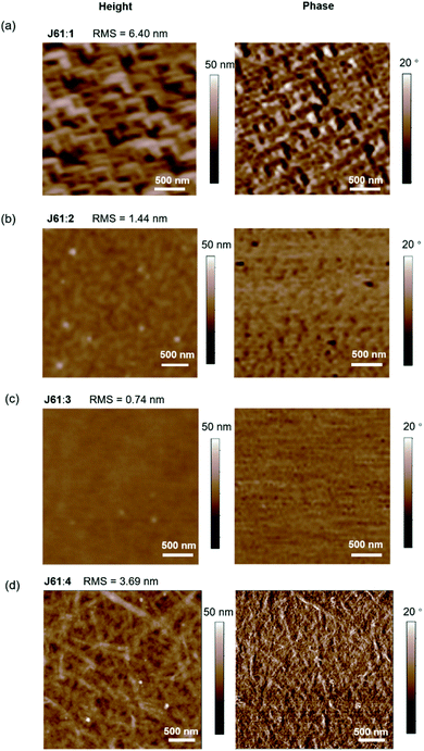 |
| | Fig. 5 AFM height and phase images of the thermally annealed J61 doped with (a) 1, (b) 2, (c) 3 and (d) 4 blend films. | |
Charge carrier recombination dynamics
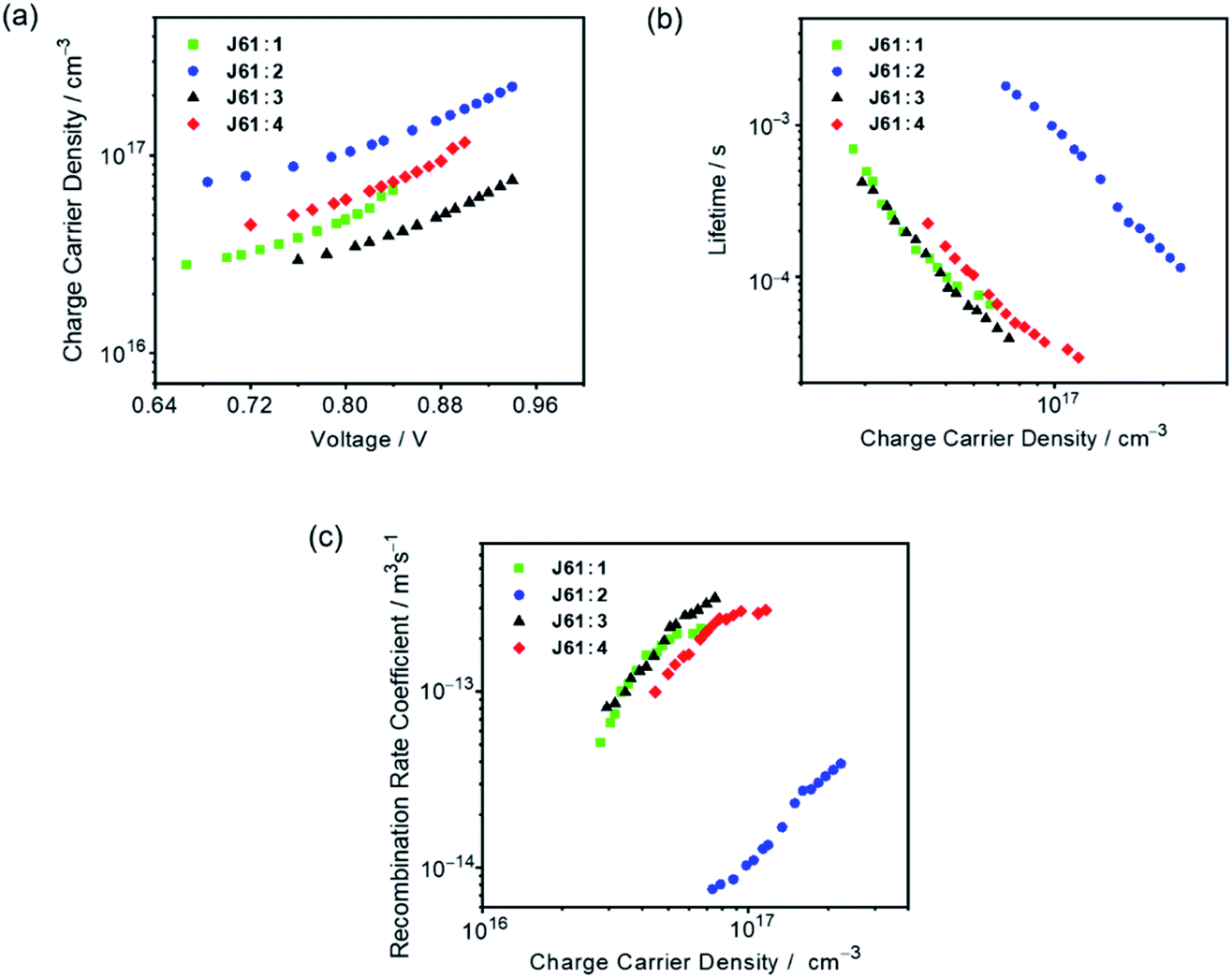
To gain quantitative insights into the charge carrier recombination dynamics within the OSC devices using J61 as the donor material, transient photocurrent (TPC) and transient photovoltage (TPV) measurements were carried out.71,72Fig. 6a shows the charge carrier densities as a function of Voc for different bias light intensities.71,73 For all the devices, the charge densities are found to follow an approximately exponential dependence on Voc over the voltage range studied. Surprisingly, at the same light intensity, the J61:2 device shows the highest charge density, which can be assigned to more efficient photocurrent generation and/or a lower non-geminate recombination rate, as shown below. On the other hand, the J61:2 device shows a low Jsc of 2.99 mA cm−2, suggesting that the overall performance is mainly limited by charge transport and extraction.55,74Fig. 6b shows the carrier lifetimes (τΔn) as a function of carrier density (n) for different bias light intensities. For all the devices, the charge carrier lifetime decreases as the charge carrier density increases, following a power-law dependence through τΔn = τΔn0n−λ, suggesting non-geminate recombination as the predominant recombination pathway.71,72,75,76 It is found that the device fabricated with the J61:2 blend shows the longest charge carrier lifetime, consistent with the charge transport/extraction limited behavior and the observed device performance parameters, such as enhanced Voc and decreased Jsc.74 Comparing 1, 3 and 4 at a given charge carrier density, the device based on J61:4 shows a longer lifetime than those of the devices fabricated with the J61:1 and J61:3 blends, corresponding to a lower decay dynamics and in good agreement with its higher charge carrier density at the same light intensity (Fig. 6a).77 In addition, by fitting τΔn(n) curves (Fig. 6b), the recombination order (λ + 1) is found to be 4.60, 4.84, 4.15, and 3.69 for the devices fabricated with the J61:1–4 blends, respectively. These empirical reaction orders, which are considerably larger than 2, can be interpreted by the shape of the density of states in combination with the spatial distribution of carriers.71,73,78,79 Particularly, the relatively smaller reaction order for the J61:4 device suggests a lower trap density, which is favorable for charge carrier extraction and transport, in accordance with its higher FF. Additionally, with the data in Fig. 6a and b, the non-geminate recombination loss can be further quantified by the recombination rate coefficient k(n), which is given by k(n) = 1/(τ(n)n) = 1/(τΔn(λ + 1)n), as a function of charge carrier density (Fig. 6c).73 The device fabricated with the J61:4 blend shows a lower non-geminate recombination rate coefficient than those with the J61:1 and J61:3 blends at the same charge carrier density. In other words, the relatively high charge carrier density and low recombination rate in the J61:4 device are believed to contribute to the device performance enhancement as compared to the other three devices using the same J61 donor material. Although the J61:2 device shows the lowest non-geminate recombination rate coefficient as a result of the high charge density and long lifetime, the device performance is limited by charge transport and extraction as mentioned above.
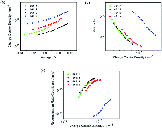 |
| | Fig. 6 Plots of (a) measured charge densities as a function of Voc for different bias light intensities, (b) derived charge carrier lifetimes as a function of charge density and (c) measured non-geminate recombination rate coefficients as a function of charge densities in the devices based on J61:1–4. | |
Organic resistive memory characteristics
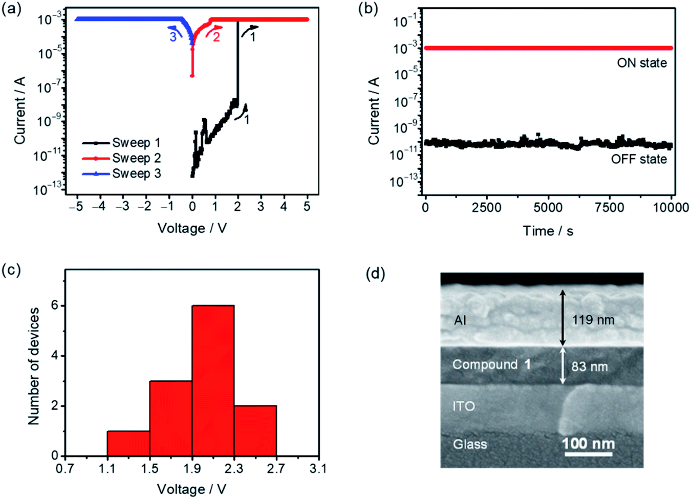
To further explore the potential applications of this class of difluoroboron(III) β-diketonate end-capped small molecules in organic electronics, 1, 3 and 4 were employed to fabricate organic resistive memory devices (see the ESI† for details). Scanning electron microscopy (SEM) of the cross-sections of the devices was performed to determine the thicknesses of the active layer and the aluminum electrode (Fig. S10†). As illustrated in Fig. 7a, when applying external voltages exceeding the threshold voltage (Vth) of ca. 2.0 V (sweep 1), the memory device of 1 is found to be switched from a low-conductivity state (“OFF” state) to a high-conductivity state (“ON” state) with a sharp current increase from 10−9 to 10−3 A. Such “ON” state can be maintained in a subsequent sweep (sweep 2), and shows good stability upon applying a reverse bias (sweep 3). In addition, the “ON” state would be relaxed to the “OFF” state after the removal of applied voltage for a week, and then switched back to the “ON” state by applying a bias again, indicative of the static random-access memory (SRAM) nature of the memory device fabricated with 1.80–82 Further examination of the stability of the two distinctive conduction states by consecutively applying a constant bias of 1 V was performed, in which no significant current degradation for both “ON” and “OFF” states for over 104 seconds is observed, indicating a high durability and reliability of the binary memory performance (Fig. 7b). The reproducibility of the device performance was also demonstrated by analyzing 12 individual cells, in which a relatively narrow Vth distribution is obtained (Fig. 7c). Binary resistive memory behavior with similar current–voltage (I–V) characteristics, stability of the ON/OFF states and distribution of the Vth was also obtained in the devices fabricated with 3 (Fig. S11†). These results suggest that the replacement of the fluorene-centered donor moiety in 1 with the IDT-centered moiety in 3 shows no notable differences in the memory behavior. In contrast, the variation of the peripheral substituent on the terminal difluoroboron(III) β-diketonate moiety has clear impacts on the Vth and stability of the memory devices. Specifically, changing the substituents from trifluoromethyl groups in 3 to cyano groups in 4 leads to a relatively higher Vth of ca. 3.0 V and lower stability of the “OFF” state when compared with those with 3 (Fig. S12†). Similar I–V characteristics are obtained by applying a reverse bias voltage. A threshold switching voltage of −2.5 V is observed in compound 1 (Fig. S13†). The resistive memory performances achieved by this series of compounds were also compared with those attained by some recently reported organic resistive memories (Table S7†). Comparable performance parameters, such as a long retention time, a high ON/OFF ratio of >103 and a narrow Vth distribution, were observed in the resistive memories based on 1, 3 and 4. These results suggest that this series of air-stable four-coordinate BF2bdk-based small molecules hold promise in serving as potential functional materials for electronic memories.
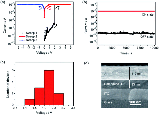 |
| | Fig. 7 (a) I–V characteristics, (b) retention time in “OFF” and “ON” states under a constant bias of 1 V, (c) distribution of the switching threshold voltage (12 devices) and (d) SEM image of the cross-section of the memory device fabricated with 1. | |
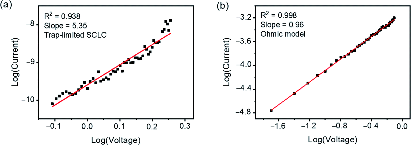
Various mechanisms, such as the charge-transfer and the charge-trapping mechanisms, have been proposed to explain the field-induced conductance switching behaviours achieved by organic active materials possessing donor–acceptor structures.80–89 In order to gain further insights into the conductance switching mechanism of memory devices fabricated with these boron(III) β-diketonate end-capped compounds, the I–V characteristics of the “OFF” and “ON” states were analyzed with appropriate charge transport models.90,91 As shown in Fig. 8, S14 and S15,† the I–V characteristics of devices fabricated with 1, 3 and 4 in the “OFF” and “ON” states can be appropriately fitted with the SCLC models (I ≈ Vm+1, m > 1)83–85 and the ohmic conduction models,86–88 respectively. Based on these results, the conductance switching of the memory devices fabricated with this series of compounds is believed to originate from the charge trapping mechanism.89,92,93 In the OFF state, the organic active layer is electrically insulating due to the presence of the electron-withdrawing boron(III) β-diketonate moieties, which can function as charge traps and impede the migration of charge carriers in the bulk material, resulting in the trap-limited SCLC conduction.92–94 When the applied bias voltage exceeds the Vth of the devices, more electrons will be injected into the active layer. As such, the trapping sites originating from the boron(III) β-diketonate moieties will be filled, and thus the newly generated charge carriers will not be affected by the traps, leading to the ohmic conduction in the ON state.92–94 From the molecular structure point of view, the stronger electron-accepting ability of the cyano substituent as compared to the trifluoromethyl substituent could increase the charge trapping properties of the terminal boron(III) β-diketonate moiety, which could therefore be responsible for the relatively higher Vth observed in 4-fabricated memory devices as compared to that observed in 3-fabricated ones. The better electron-accepting ability of boron(III) β-diketonate moieties in 4 is also supported by the electrostatic potential (ESP) surfaces obtained from DFT calculations, in which a lower electron density is found with the cyano substituent when compared with the trifluoromethyl substituent (see the ESI†).
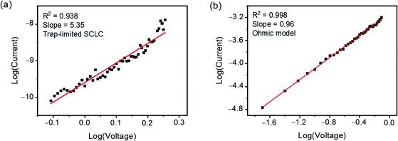 |
| | Fig. 8 Plots of log(I) vs. log(V) obtained by fitting the I–V characteristics of (a) the “OFF” state (from 0.78 to 1.80 V) and (b) the “ON” state (from 0.02 to 0.78 V) of the memory device fabricated with 1. | |
Conclusion
In summary, BF2bdk-based molecular materials 1–4 have been applied as A–D–A type NFAs for the first time. It is found that the introduction of an appropriate electron-donating core and simple modification of peripheral substituents on the BF2bdk can fine-tune their photophysical and electrochemical properties. Particularly for 4, in which IDT serves as the central donor unit and the cyano-substituted BF2bdk serves as the terminal acceptor unit, a broad absorption profile extending to 782 nm and a low-lying LUMO energy level of −3.72 eV have been realized. Moreover, these BF2bdk end-capped electron acceptors feature excellent electron-transport properties with a μe of up to 7.49 × 10⁻⁴ cm2 V−1 s−1 in the bulk heterojunction blend. A PCE of 4.31% for the device based on J52:4 has been achieved, which is comparable to those of high-performance IDT-centered electron acceptors for OSCs, demonstrating the potential of the BF2bdk as a promising electron-accepting building block in the construction of A–D–A type small-molecule NFAs for OSCs. In addition, organic resistive memory devices fabricated with these BF2bdk end-capped compounds are found to follow a charge-trapping mechanism, resulting in stable binary memory devices with distinctive ON/OFF current ratios > 106, as well as a tunable Vth achieved by changing the electron-accepting end-groups from trifluoromethyl to cyano moieties.
Conflicts of interest
There are no conflicts to declare.
Acknowledgements
V. W.-W. Y. acknowledges the support from the University Research Committee (URC) Strategically Oriented Research Theme (SORT) on Functional Materials for Molecular Electronics of The University of Hong Kong (HKU). This work has been supported by the Guangdong-Hong Kong-Macao Joint Laboratory of Optoelectronic and Magnetic Functional Materials (2019B121205002) and a General Research Fund (GRF) grant from the Research Grants Council of the Hong Kong Special Administrative Region, P. R. China (HKU 17306219). P. Li acknowledges the receipt of a postgraduate studentship from The University of Hong Kong. The University Development Fund of The University of Hong Kong is acknowledged for funding the Bruker D8 VENTURE MetalJet Photon II CPAD X-Ray diffractometer. Dr L.-Y. Yao is acknowledged for his helpful discussion and assistance in the X-ray crystal structure study. Dr Maggie Ng is thanked for her help in the computational studies. Dr C.-O. Ng and Dr C.-C. Ko from the City University of Hong Kong are acknowledged for their help with the DSC measurements.
References
- B. C. Thompson and J. M. J. Fréchet, Angew. Chem., Int. Ed., 2008, 47, 58–77 CrossRef CAS.
- Y. Li, Acc. Chem. Res., 2012, 45, 723–733 CrossRef CAS.
- Y. Huang, E. J. Kramer, A. J. Heeger and G. C. Bazan, Chem. Rev., 2014, 114, 7006–7043 CrossRef CAS.
- R. Ganesamoorthy, G. Sathiyan and P. Sakthivel, Sol. Energy Mater. Sol. Cells, 2017, 161, 102–148 CrossRef CAS.
- H. Gaspar, F. Figueira, L. Pereira, A. Mendes, J. C. Viana and G. Bernardo, Materials, 2018, 11, 2560 CrossRef.
- G. Sauvé and R. Fernando, J. Phys. Chem. Lett., 2015, 6, 3770–3780 CrossRef.
- C. B. Nielsen, S. Holliday, H.-Y. Chen, S. J. Cryer and I. McCulloch, Acc. Chem. Res., 2015, 48, 2803–2812 CrossRef CAS.
- G. Zhang, J. Zhao, P. C. Y. Chow, K. Jiang, J. Zhang, Z. Zhu, J. Zhang, F. Huang and H. Yan, Chem. Rev., 2018, 118, 3447–3507 CrossRef CAS.
- H. Sun, F. Chen and Z.-K. Chen, Mater. Today, 2019, 24, 94–118 CrossRef CAS.
- J. Hou, O. Inganäs, R. H. Friend and F. Gao, Nat. Mater., 2018, 17, 119–128 CrossRef CAS.
- C. Cui, Front. Chem., 2018, 6, 404 CrossRef CAS.
- S. K. Mellerup and S. Wang, Trends Chem., 2019, 1, 77–89 CrossRef.
- Y.-L. Rao and S. Wang, Inorg. Chem., 2011, 50, 12263–12274 CrossRef CAS.
- Z. Huang, S. Wang, R. D. Dewhurst, N. V. Ignat’ev, M. Finze and H. Braunschweig, Angew. Chem., Int. Ed., 2020, 59, 8800–8816 CrossRef CAS.
- Y. Yu, C. Dong, A. F. Alahmadi, B. Meng, J. Liu, F. Jäkle and L. Wang, J. Mater. Chem. C, 2019, 7, 7427–7432 RSC.
- T. Welsh, A. Laventure, A. Alahmadi, G. Zhang, T. Baumgartner, Y. Zou, F. Jäkle and G. C. Welch, ACS Appl. Energy Mater., 2019, 2, 1229–1240 CrossRef CAS.
- M. M. Morgan, M. Nazari, T. Pickl, J. M. Rautiainen, H. M. Tuononen, W. Piers, G. C. Welch and B. S. Gelfand, Chem. Commun., 2019, 55, 11095–11098 RSC.
- J. M. Farrell, C. Mützel, D. Bialas, M. Rudolf, K. Menekse, A.-M. Krause, M. Stolte and F. Würthner, J. Am. Chem. Soc., 2019, 141, 9096–9104 CrossRef CAS.
- C. Duan, G. Zango, M. García Iglesias, F. J. M. Colberts, M. M. Wienk, M. V. Martínez-Díaz, R. A. J. Janssen and T. Torres, Angew. Chem., Int. Ed., 2017, 56, 148–152 CrossRef CAS.
- A. M. Poe, A. M. Della Pelle, A. V. Subrahmanyam, W. White, G. Wantz and S. Thayumanavan, Chem. Commun., 2014, 50, 2913–2915 RSC.
- J. Liu, F. Liu and L. Wang, Org. Chem. Front., 2019, 6, 1996–2003 RSC.
- F. Liu, Z. Ding, J. Liu and L. Wang, Chem. Commun., 2017, 53, 12213–12216 RSC.
- K. Tanaka and Y. Chujo, NPG Asia Mater., 2015, 7, e223 CrossRef CAS.
- Y. Sun, D. Rohde, Y. Liu, L. Wan, Y. Wang, W. Wu, C. Di, G. Yu and D. Zhu, J. Mater. Chem., 2006, 16, 4499–4503 RSC.
- K. Ono, J. Hashizume, H. Yamaguchi, M. Tomura, J.-i. Nishida and Y. Yamashita, Org. Lett., 2009, 11, 4326–4329 CrossRef CAS.
- K. Ono, H. Yamaguchi, K. Taga, K. Saito, J.-i. Nishida and Y. Yamashita, Org. Lett., 2009, 11, 149–152 CrossRef CAS.
- K. Ono, A. Nakashima, Y. Tsuji, T. Kinoshita, M. Tomura, J.-i. Nishida and Y. Yamashita, Chem.–Eur. J., 2010, 16, 13539–13546 CrossRef CAS.
- B. Domercq, C. Grasso, J.-L. Maldonado, M. Halik, S. Barlow, S. R. Marder and B. Kippelen, J. Phys. Chem. B, 2004, 108, 8647–8651 CrossRef CAS.
- D.-H. Kim, A. D’Aléo, X.-K. Chen, A. D. S. Sandanayaka, D. Yao, L. Zhao, T. Komino, E. Zaborova, G. Canard, Y. Tsuchiya, E. Choi, J. W. Wu, F. Fages, J.-L. Brédas, J.-C. Ribierre and C. Adachi, Nat. Photonics, 2018, 12, 98–104 CrossRef CAS.
- H. Zhang, P.-Z. Chen, L.-Y. Niu and Q.-Z. Yang, Mater. Chem. Front., 2020, 4, 285–291 RSC.
- C.-T. Poon, D. Wu, W. H. Lam and V. W.-W. Yam, Angew. Chem., Int. Ed., 2015, 54, 10569–10573 CrossRef CAS.
- C.-T. Poon, D. Wu and V. W.-W. Yam, Angew. Chem., Int. Ed., 2016, 55, 3647–3651 CrossRef CAS.
- C.-T. Poon, W. H. Lam, H.-L. Wong and V. W.-W. Yam, J. Am. Chem. Soc., 2010, 132, 13992–13993 CrossRef CAS.
- C.-T. Poon, W. H. Lam and V. W.-W. Yam, Chem.–Eur. J., 2013, 19, 3467–3476 CrossRef CAS.
- C.-T. Poon, W. H. Lam and V. W.-W. Yam, J. Am. Chem. Soc., 2011, 133, 19622–19625 CrossRef CAS.
- H. Chan, H.-L. Wong, M. Ng, C.-T. Poon and V. W.-W. Yam, J. Am. Chem. Soc., 2017, 139, 7256–7263 CrossRef CAS.
- C.-L. Wong, C.-T. Poon and V. W.-W. Yam, Organometallics, 2017, 36, 2661–2669 CrossRef CAS.
- P. Li, H. Chan, S.-L. Lai, M. Ng, M.-Y. Chan and V. W. W. Yam, Angew. Chem., Int. Ed., 2019, 58, 9088–9094 CrossRef CAS.
- M.-J. Baek, W. Jang, S.-H. Lee and Y.-S. Lee, Synth. Met., 2012, 161, 2785–2791 CrossRef.
- Y.-C. Chen, C.-Y. Yu, Y.-L. Fan, L.-I. Hung, C.-P. Chen and C. Ting, Chem. Commun., 2010, 46, 6503–6505 RSC.
- A. Jaafari, V. Ouzeau, M. Ely, F. Rodriguez, K. Chane-ching, A. Yassar and J. J. Aaron, Synth. Met., 2004, 147, 183–189 CrossRef CAS.
- H. Bai, Y. Wang, P. Cheng, J. Wang, Y. Wu, J. Hou and X. Zhan, J. Mater. Chem. A, 2015, 3, 1910–1914 RSC.
- S. Holliday, R. S. Ashraf, C. B. Nielsen, M. Kirkus, J. A. Röhr, C.-H. Tan, E. Collado-Fregoso, A.-C. Knall, J. R. Durrant, J. Nelson and I. McCulloch, J. Am. Chem. Soc., 2015, 137, 898–904 CrossRef CAS.
- P. M. Beaujuge and J. M. J. Fréchet, J. Am. Chem. Soc., 2011, 133, 20009–20029 CrossRef CAS.
- M. Mas-Torrent and C. Rovira, Chem. Rev., 2011, 111, 4833–4856 CrossRef CAS.
- C. B. Nielsen, S. Holliday, H.-Y. Chen, S. J. Cryer and I. McCulloch, Acc. Chem. Res., 2015, 48, 2803–2812 CrossRef CAS.
- Suman and S. P. Singh, J. Mater. Chem. A, 2019, 7, 22701–22729 RSC.
- C. Cui, Front. Chem., 2018, 6, 1–11 Search PubMed.
- G. Han, Y. Guo, X. Song, Y. Wang and Y. Yi, J. Mater. Chem. C, 2017, 5, 4852–4857 RSC.
- D. Mo, H. Chen, J. Zhou, N. Tang, L. Han, Y. Zhu, P. Chao, H. Lai, Z. Xie and F. He, J. Mater. Chem. A, 2020, 8, 8903–8912 RSC.
- H. Lai, Q. Zhao, Z. Chen, H. Chen, P. Chao, Y. Zhu, Y. Lang, N. Zhen, D. Mo, Y. Zhang and F. He, Joule, 2020, 4, 688–700 CrossRef CAS.
- C. Cui, X. Guo, J. Min, B. Guo, X. Cheng, M. Zhang, C. J. Brabec and Y. Li, Adv. Mater., 2015, 27, 7469–7475 CrossRef CAS.
- H. Bin, Z.-G. Zhang, L. Gao, S. Chen, L. Zhong, L. Xue, C. Yang and Y. Li, J. Am. Chem. Soc., 2016, 138, 4657–4664 CrossRef CAS.
- Y. He and Y. Li, Phys. Chem. Chem. Phys., 2011, 13, 1970–1983 RSC.
- W. Wang, B. Zhao, Z. Cong, Y. Xie, H. Wu, Q. Liang, S. Liu, F. Liu, C. Gao, H. Wu and Y. Cao, ACS Energy Lett., 2018, 3, 1499–1507 CrossRef CAS.
- A. Rao, P. C. Y. Chow, S. Gélinas, C. W. Schlenker, C.-Z. Li, H.-L. Yip, A. K. Y. Jen, D. S. Ginger and R. H. Friend, Nature, 2013, 500, 435–439 CrossRef CAS.
- M. Li, Y. Liu, W. Ni, F. Liu, H. Feng, Y. Zhang, T. Liu, H. Zhang, X. Wan, B. Kan, Q. Zhang, T. P. Russell and Y. Chen, J. Mater. Chem. A, 2016, 4, 10409–10413 RSC.
- H. Bai, Y. Wang, P. Cheng, J. Wang, Y. Wu, J. Hou and X. Zhan, J. Mater. Chem. A, 2015, 3, 1910–1914 RSC.
- Y. Li, M. Gu, Z. Pan, B. Zhang, X. Yang, J. Gu and Y. Chen, J. Mater. Chem. A, 2017, 5, 10798–10814 RSC.
- A. Dieckmann, H. Bässler and P. M. Borsenberger, J. Chem. Phys., 1993, 99, 8136–8141 CrossRef CAS.
- D. Hertel and H. Bässler, ChemPhysChem, 2008, 9, 666–688 CrossRef CAS.
- H. Bürckstümmer, E. V. Tulyakova, M. Deppisch, M. R. Lenze, N. M. Kronenberg, M. Gsänger, M. Stolte, K. Meerholz and F. Würthner, Angew. Chem., Int. Ed., 2011, 50, 11628–11632 CrossRef.
- H.-C. Ting, Y.-H. Chen, L.-Y. Lin, S.-H. Chou, Y.-H. Liu, H.-W. Lin and K.-T. Wong, ChemSusChem, 2014, 7, 457–465 CrossRef CAS.
- Y. Yang, Z.-G. Zhang, H. Bin, S. Chen, L. Gao, L. Xue, C. Yang and Y. Li, J. Am. Chem. Soc., 2016, 138, 15011–15018 CrossRef CAS.
- D. Bartesaghi, I. d. C. Pérez, J. Kniepert, S. Roland, M. Turbiez, D. Neher and L. J. A. Koster, Nat. Commun., 2015, 6, 7083 CrossRef CAS.
- M. Hao, T. Liu, Y. Xiao, L.-K. Ma, G. Zhang, C. Zhong, Z. Chen, Z. Luo, X. Lu, H. Yan, L. Wang and C. Yang, Chem. Mater., 2019, 31, 1752–1760 CrossRef CAS.
- D. Veldman, Ö. İpek, S. C. J. Meskers, J. Sweelssen, M. M. Koetse, S. C. Veenstra, J. M. Kroon, S. S. van Bavel, J. Loos and R. A. J. Janssen, J. Am. Chem. Soc., 2008, 130, 7721–7735 CrossRef CAS.
- W. Huang, E. Gann, N. Chandrasekaran, S. K. K. Prasad, S.-Y. Chang, L. Thomsen, D. Kabra, J. M. Hodgkiss, Y.-B. Cheng, Y. Yang and C. R. McNeill, Adv. Energy Mater., 2017, 7, 1602197 CrossRef.
- Y. Jia, Y. Zhang, W. Jiang, B. Su, C. Liu, E. Zhu and G. Che, J. Mater. Chem. A, 2019, 7, 10905–10911 RSC.
- H. Wu, B. Zhao, H. Zhao, L. Wang, W. Wang, Z. Cong, J. Liu, W. Ma and C. Gao, ACS Appl. Mater. Interfaces, 2020, 12, 789–797 CrossRef CAS.
- C. G. Shuttle, B. O'Regan, A. M. Ballantyne, J. Nelson, D. D. C. Bradley, J. d. Mello and J. R. Durrant, Appl. Phys. Lett., 2008, 92, 093311 CrossRef.
- J. Yan, Q. Liang, K. Liu, J. Miao, H. Chen, S. Liu, Z. He, H. Wu, J. Wang and Y. Cao, ACS Energy Lett., 2017, 2, 14–21 CrossRef CAS.
- R. Hamilton, C. G. Shuttle, B. O'Regan, T. C. Hammant, J. Nelson and J. R. Durrant, J. Phys. Chem. Lett., 2010, 1, 1432–1436 CrossRef CAS.
- Q. Zhang, J. J. Rech, L. Yan, Q. Liang, Z. Peng, H. Ade, H. Wu and W. You, ACS Appl. Polym. Mater., 2019, 1, 3313–3322 CrossRef CAS.
- A. Maurano, C. G. Shuttle, R. Hamilton, A. M. Ballantyne, J. Nelson, W. Zhang, M. Heeney and J. R. Durrant, J. Phys. Chem. C, 2011, 115, 5947–5957 CrossRef CAS.
- A. Maurano, R. Hamilton, C. G. Shuttle, A. M. Ballantyne, J. Nelson, B. O'Regan, W. Zhang, I. McCulloch, H. Azimi, M. Morana, C. J. Brabec and J. R. Durrant, Adv. Mater., 2010, 22, 4987–4992 CrossRef CAS.
- C. G. Shuttle, A. Maurano, R. Hamilton, B. O'Regan, J. C. d. Mello and J. R. Durrant, Appl. Phys. Lett., 2008, 93, 183501 CrossRef.
- T. Kirchartz, B. E. Pieters, J. Kirkpatrick, U. Rau and J. Nelson, Phys. Rev. B: Condens. Matter Mater. Phys., 2011, 83, 115209 CrossRef.
- T. Kirchartz and J. Nelson, Phys. Rev. B: Condens. Matter Mater. Phys., 2012, 86, 165201 CrossRef.
- Q.-D. Ling, D.-J. Liaw, C. Zhu, D. S.-H. Chan, E.-T. Kang and K.-G. Neoh, Prog. Polym. Sci., 2008, 33, 917–978 CrossRef CAS.
- R. Waser, R. Dittmann, G. Staikov and K. Szot, Adv. Mater., 2009, 21, 2632–2663 CrossRef CAS.
- W.-P. Lin, S.-J. Liu, T. Gong, Q. Zhao and W. Huang, Adv. Mater., 2014, 26, 570–606 CrossRef CAS.
- G. Wen, Z. Ren, D. Sun, T. Zhang, L. Liu and S. Yan, Adv. Funct. Mater., 2014, 24, 3446–3455 CrossRef CAS.
-
M. A. Lampert and R. B. Schilling, Semiconduct. Semimet, ed. R. K. Willardson and A. C. Beer, Elsevier, 1970, vol. 6, pp. 1–96 Search PubMed.
- P. N. Murgatroyd, J. Phys. D: Appl. Phys., 1970, 3, 151–156 CrossRef.
- W. Wang, T. Lee and M. A. Reed, Phys. Rev. B: Condens. Matter Mater. Phys., 2003, 68, 035416 CrossRef.
- F. Pan, S. Gao, C. Chen, C. Song and F. Zeng, Mater. Sci. Eng., R, 2014, 83, 1–59 CrossRef.
- E. W. Lim and R. Ismail, Electronics, 2015, 4, 586–613 CrossRef CAS.
- Q.-D. Ling, D.-J. Liaw, C. Zhu, D. S.-H. Chan, E.-T. Kang and K.-G. Neoh, Prog. Polym. Sci., 2008, 33, 917–978 CrossRef CAS.
- P. Stallinga, Adv. Mater., 2011, 23, 3356–3362 CrossRef CAS.
- Q.-D. Ling, D.-J. Liaw, C. Zhu, D. S.-H. Chan, E.-T. Kang and K.-G. Neoh, Prog. Polym. Sci., 2008, 33, 917–978 CrossRef CAS.
- Y. Zhou, S.-T. Han, Y. Yan, L. Zhou, L.-B. Huang, J. Zhuang, P. Sonar and V. A. L. Roy, Sci. Rep., 2015, 5, 10683 CrossRef CAS.
- Q.-D. Ling, Y. Song, S.-L. Lim, E. Y.-H. Teo, Y.-P. Tan, C. Zhu, D. S. H. Chan, D.-L. Kwong, E.-T. Kang and K.-G. Neoh, Angew. Chem., Int. Ed., 2006, 45, 2947–2951 CrossRef CAS.
- P. Stallinga, Adv. Mater., 2011, 23, 3356–3362 CrossRef CAS.
Footnote |
| † Electronic supplementary information (ESI) available: Synthesis and characterization, X-ray crystal structure study, thermogravimetric analysis and differential scanning calorimetry, optical properties, electrochemical studies, device fabrication and characterization, and computational details and studies. CCDC 1960933. For ESI and crystallographic data in CIF or other electronic format see DOI: 10.1039/d0sc04047a |
|
| This journal is © The Royal Society of Chemistry 2020 |
Click here to see how this site uses Cookies. View our privacy policy here. 
 Open Access Article
 This Open Access Article is licensed under a Creative Commons Attribution-Non Commercial 3.0 Unported Licence
 a,
Quanbin
Liang
b,
Eugene Yau-Hin
Hong
a,
Chin-Yiu
Chan
a,
Yat-Hin
Cheng
a,
Ming-Yi
Leung
a,
Mei-Yee
Chan
a,
Quanbin
Liang
b,
Eugene Yau-Hin
Hong
a,
Chin-Yiu
Chan
a,
Yat-Hin
Cheng
a,
Ming-Yi
Leung
a,
Mei-Yee
Chan