
Microfluidic surface-enhanced infrared spectroscopy with semiconductor plasmonics for the fingerprint region
Mario
Bomers
 a,
Benoît
Charlot
a,
Franziska
Barho
a,
Antoine
Chanuel
a,
Aude
Mezy
b,
Laurent
Cerutti
a,
Fernando
Gonzalez-Posada
a and
Thierry
Taliercio
*a
a,
Benoît
Charlot
a,
Franziska
Barho
a,
Antoine
Chanuel
a,
Aude
Mezy
b,
Laurent
Cerutti
a,
Fernando
Gonzalez-Posada
a and
Thierry
Taliercio
*a
aIES, Université de Montpellier, CNRS, Montpellier, France. E-mail: thierry.taliercio@umontpellier.fr
bSiKÉMIA, F-34095 Montpellier, France
First published on 15th November 2019
Abstract
The combination of semiconductor plasmonics with microfluidics allows surface-enhanced infrared spectroscopy of molecules in the flow regime. Exploiting semiconductor plasmonics enables surface-enhanced mid-IR spectroscopy from 4 μm to 20 μm and accesses the so-called molecular fingerprint region from 6.7 μm to 20 μm (1500–500 cm−1). Besides addressing the whole fingerprint region and allowing the identification of molecules by database comparison, the III–V semiconductor material class allows potentially an integration of semiconductor-based IR-sources, IR-detectors and IR-resonators on-chip. Miniaturized plasmonic enhanced microfluidic mid-IR spectrometry has great potential to analyse and identify minute amounts of molecules in the flow regime. This work describes technological processing to combine semiconductor plasmonics and microfluidics. Two proof-of-concept prototypes were experimentally realized and subsequently tested. Measured mid-IR spectra allow to clearly distinguish ethanol and water by their respective IR-absorption characteristics when inserted into the microfluidic flow chamber. Additionally, a semiconductor surface plasmon resonance shift can be observed according to the inserted solvent. Finally, the formation of a self-assembled monolayer under flow conditions is demonstrated by an observable mid-IR surface plasmon resonance shift of 6 ± 1 cm−1 (140 ± 23 nm).
Introduction
This work presents novel materials for plasmonic enhanced microfluidic infrared spectroscopy which allows reaction analysis and monitoring under flow conditions. In the context of on-chip infrared spectroscopy,1 the combination of semiconductor plasmonics and microfluidics addresses two challenges: on the one hand the use of innovative materials and on the other hand the use of sensitivity enhancing plasmonic structures to go beyond the enhancement effects of exploiting attenuated total reflection (ATR). At least two different application areas are conceivable. First, the further development of the semiconductor plasmonic sensor and integration as process analytical technology (PAT) for trace analysis of reaction products in a so-called laboratory of the future approach.2 Second, further development on integration of IR-detector and IR-source on-chip to finally address global public health by development of portable on-chip microfluidic diagnostic devices.3 Innovative approaches exploit the widespread portable visible light sources and portable visible light detectors in smartphones for label-free bio-detection.4 The underlying detection principle is the shift of a resonant frequency of a specifically designed plasmonic or photonic structure.5 Despite good sensitivity, this technique does not provide full spectral information. For this reason, it is still challenging to create portable vibrational spectroscopy devices which allow Raman spectroscopy or IR spectroscopy on-chip. Concurrently to the maturing of microfluidic fabrication technology,6,7 the advancements of silicon manufacturing techniques might allow relatively cheap mass-production of silicon photonic circuits as the backbone of a miniaturized Raman spectroscopy device.8 As Raman spectroscopy works in the visible range of light, the lab-on-chip approach benefits from the wide accessibility of transparent material for microfluidic fabrication and from the widespread of portable light sources and light detectors. Nevertheless, infrared spectroscopy, as complementary vibrational spectroscopy technique to Raman spectroscopy, offers some advantages. Infrared light is less harmful to molecules than intense laser light necessary for Raman scattering. Additionally, a typical cross-section for infrared absorption is with approximately 10−20 cm2 much higher than a typical cross-section for Raman scattering (10−29 cm2), thus infrared spectroscopy is intrinsically by several orders more sensitive.9 The lower scattering cross-section of the Raman process can be compensated by surface-enhanced Raman scattering (SERS), where the electric field is strongly enhanced at the surface of resonant nanostructures and decays rapidly away from the surface.10 In combination with microfluidics, an elegant way to obtain SERS-signal for low concentration trace analysis consists in mixing analyte molecules and plasmonic particles in a microdroplet sensor.11,12 Another way of using SERS to improve immunoassays is to address nonspecific adsorption by specifically designed fluorophore-integrated gold/silver nanoshells as SERS nanotags.13 Analogous to surface-enhanced Raman spectroscopy (SERS) for visible light, surface-enhanced infrared absorption (SEIRA) spectroscopy exists for the infrared.14 The motivation of exploiting specifically designed plasmonic resonators for SEIRA is to obtain more measurement signal for measuring low concentrations of molecules in the proximity of the resonators' surface, e.g. to trace the formation of self-assembled monolayers (SAM) of organic molecules.Gold is so far the most prominent material for fabricating plasmonic resonators in the IR-range, but doping levels in the 1019 cm−3 range transform III–V semiconductors, in particular InAs and InAsSb, to ideal mid-IR plasmonic materials.15 It was shown that heavily Si-doped InAs(Sb) not only rivals gold in the mid-IR range in terms of larger density of hot-spots and thus better signal to noise ratio for plasmonic applications,16 but also in terms of good compatibility with silicon technology. A theoretical study showed that in the infrared range, the better performance of degenerate semiconductors versus conventional metals in terms of hot-spot density is a general trend.17 Not only heavily Si-doped III–V semiconductors but as well heavily Ga-doped ZnO and heavily doped germanium allows the fabrication of plasmonic sensors which can compete with state-of-the-art sensors based on gold.18,19 Finally, it is a question of choosing the right degenerate semiconductor material for the envisaged spectral range. InAs and InAsSb are particularly suited to provide plasmonic resonances in the molecular fingerprint region from 5 μm to 20 μm.20,21 Despite these advantages of InAs and InAsSb for SEIRA, gold and its chemical inertness can be used in a wider range of different chemical environments. While InAs and InAsSb are stable in water and organic solvents, aqueous buffer solutions (pH = 5 or pH = 9) lead, without additional surface passivation, to Indium leakage.22 In particular, when InAsSb is grown on GaSb, the oxidation process of GaSb in water is another factor to consider for potential sensing applications.23 Despite the restriction to a smaller range of different chemical environments, InAs and InAsSb based plasmonic resonators have the important advantage of being combinable with III–V semiconductor-based optoelectronic devices such as IR-lasers or IR-light detectors.24 III–V semiconductor as InAs/GaSb type-II superlattice structures are used as IR-detector material25 and widely tunable quantum cascade lasers based on III–V semiconductors (AlInAs/GaInAs)26 or InAs/AlSb-based quantum cascade lasers grown on silicon can serve as IR-light sources.27 More information on semiconductor infrared plasmonics can be found in a recent review article.28
In the context of on-chip infrared spectroscopy, a major challenge is to bypass the lacking IR-transparency of glass and poly(dimethylsiloxane) (PDMS) in the so-called molecular fingerprint region from 6.7 μm to 20 μm (1500–500 cm−1) by using IR-transparent materials. Calcium fluoride (CaF2) has shown good compatibility with microfluidics and has high transmission values in the order of 90% from the visible range of light till IR-light around 10 μm. Most undoped III–V semiconductors are with transmission values around 50% less transparent than Calcium fluoride, but they allow to access the whole molecular fingerprint region till 20 μm. To circumvent the challenge of transmission through not IR-transparent polymers, the attenuated total reflection (ATR) technique can be applied for IR-transparent substrates coated with thin layers of metal.29 Generally, infrared spectroscopy in the attenuated total reflection (ATR) configuration can be combined with an infrared focal plane array (FPA) detector to allow chemical imaging of biological systems.30 Whether in ATR or transmission configuration, the combination of microfluidics and Fourier-transform infrared (FT-IR) spectroscopy allows imaging of reactions in a controlled flow regime.31–33 Besides circumventing the lack of IR-transmission through PDMS, another advantage of the ATR-technique is the high-surface sensitivity and the avoidance of signal saturation originating from solvent IR-absorption bands.34 The possibility to further improve the sensitivity of infrared microfluidic spectroscopy was demonstrated by combining a plasmonic resonator based SEIRA-spectroscopy system with microfluidics.35 This pioneering SEIRA on-chip work exploited gold plasmonic resonators on an infrared transparent CaF2-substrate. The successful combination of resonant nanoantenna systems and microfluidics allows in situ ultra-sensitive spectroscopy of biomolecule interactions in real time.36 Recent technological advances culminated in nanoresonators combined with nanometric flow chambers for SEIRA applications.37 This research field is still very active and applications in the field of studying dynamic lipid membrane processes demonstrate the great potential of these nanoresonator systems combined with microfluidics.38
This article demonstrates that semiconductor plasmonic resonators can be combined with microfluidics. It has to be seen in the context of other semiconductor mid-infrared on-chip sensing concepts39 such as for example germanium-based semiconductor mid-infrared waveguide sensors integrated with a microfluidic chip for cocaine detection.40 Equally to germanium-based approaches, the binary InAs or the ternary InAsSb can be grown on semiconductor substrates such as III–V semiconductor substrates or on silicon.27,41 This allows a combination with III–V semiconductor-based mid-IR waveguides.42
In the following, the combination of heavily Si-doped InAs based plasmonic resonators on top of an IR-transparent InAs substrate with PDMS based microfluidics is demonstrated. Two microfluidic devices were fabricated and tested. In particular, the so-called backside configuration is suited for surface-enhanced IR-spectroscopy as demonstrated by measuring the alcohol content of a liquid in the flow regime and by measuring the formation of a self-assembled monolayer on the resonators' surface.
Results and discussion
Design and fabrication of microfluidic devices
Microfluidic devices fabricated by soft-lithography are often based on polymers such as PDMS. Such microfluidic devices are transparent for visible light but not for IR-light, due to IR-absorption of this polymer. Two different solutions are proposed to allow IR-spectroscopy of microfluidic devices combining semiconductor plasmonic resonators with polymer-based microfluidic circuits: first, the microfluidic device in the backside reflection configuration shown in Fig. 1 and second the microfluidic device in transmission configuration shown in Fig. 3. The key feature in both designs is the inclusion of a SiNx-layer (alternatively a SiO2-layer) in between the semiconductors (InAs) top surface and the bottom surface of the polymer block (PDMS-based) with the imprinted microfluidic liquid chamber (width of 3 mm and length of 3 mm). The deposition of the 200 nm thin SiNx-layer is necessary as adhesion layer for permanent bonding of PDMS because the InAs surface could not be oxygen plasma-activated in the sense that a sufficient amount of surface radicals was created to allow subsequent bonding with the surface-radicals of a plasma-activated PDMS layer. Only with the intermediate SiNx-layer deposited on top of the InAs-substrate a sufficiently strong bonding for the subsequent microfluidic measurements was obtained. More details on the process parameters can be found in the Materials and methods section.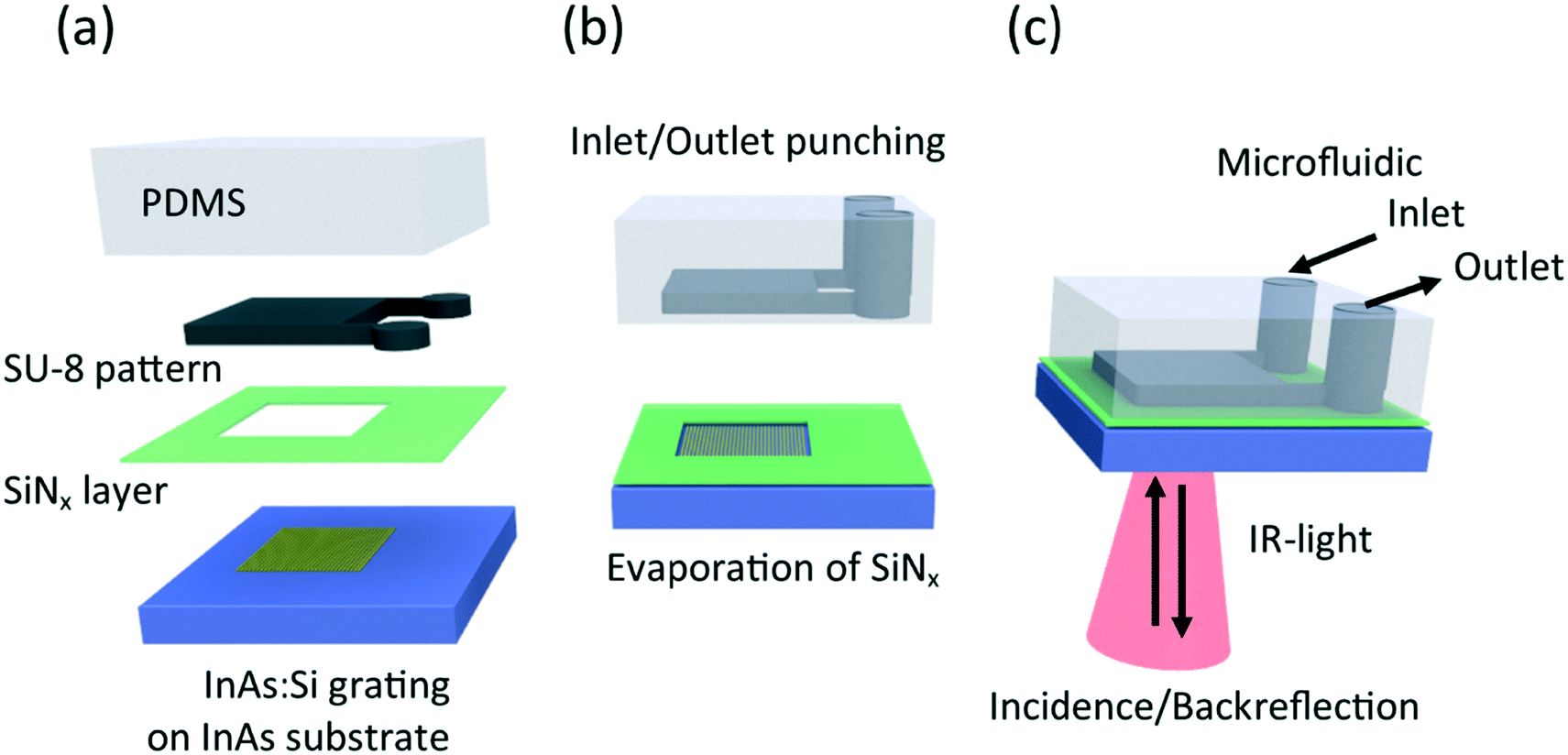 | ||
| Fig. 1 Instruction for assembling a semiconductor plasmonic resonator system with a soft lithography (PDMS) produced microfluidic system for backreflection IR-spectroscopy applications. (a) The lithographically produced SU-8 pattern defines the PDMS casting mould of the later liquid spectroscopy chamber. The SiNx layer evaporated onto the III–V semiconductor layer has an opening due to shadow masking at the position of the plasmonic InAs:Si grating. (b) After the elastomeric PDMS is stripped from the SU-8, additional inlet and outlet channels are punched into the PDMS layer. (c) The final assembling steps consists in combining the PDMS layer with the SiNx layer after plasma activation of both contact surfaces to create bond forming surface radicals. The infrared beam path where the IR-light is incident and back-reflected through the backside of the InAs substrate is shown for illustration. | ||
The backside configuration gets its name from the incident and back-reflected IR-light shown in Fig. 1(c). The beam path is sketched in red and it can be seen that the incident IR-light is transmitted through the InAs-substrate, then back-reflected at the interface of plasmonic resonators and liquid chamber and finally, after another transmission through the InAs-substrate, collected by an IR microscope coupled to an IR spectrometer operating in reflection mode. In the same figure, the microfluidic inlet and outlet channels are represented. The fabrication of the microfluidic circuit sketched in Fig. 1(a) and (b) is a standard process, where photolithography and a specifically designed mask were used to write the microfluidic pattern with the photopolymer SU-8 on a silicon substrate. The casting of PDMS, followed by a low-pressure treatment to evacuate air bubbles and by a baking step led to an imprint of the microfluidic circuit into the block of PDMS. The PDMS was stripped off from the SU-8 photopolymer and from the substrate and finally inlet and outlet were punched into the PDMS.
Concurrently to the microfluidic fabrication, the semiconductor plasmonic resonators were fabricated. The process started with molecular beam epitaxy (MBE) to create a 100 nm thin layer of heavily Si-doped InAs on top of a commercially available residually-doped InAs substrate. The low residual doping of the substrate guaranteed good transparency in the mid-IR range of light and the heavily-doped toplayer led to metallic, i.e. plasmonic behaviour of this layer. A grating structure with a ribbon width of 750 nm and a grating period of 1800 nm was patterned by photolithography and dry etching. A representative scanning electron microscopy (SEM) image is shown in Fig. 2(a). As dry etching led to some under etching, the depth of the wells in between two ribbons is 150 nm. The plasmonic resonators, defined by the thickness of the 100 nm thin layer of heavily Si-doped InAs, are therefore standing on a 50 nm high pedestal of non-doped InAs. By optical characterization of the as-grown material a doping gradient was observed for the 100 nm Si-doped InAs toplayer. Further information and relevant process parameters can be found in the Materials and methods section. A crucial step during the plasma-enhanced chemical vapor deposition (PECVD) of the 200 nm thin SiNx-layer on top of the InAs-substrate was to use a shadow mask, placed on top of the heavily Si-doped grating structure during the deposition process, to protect it from SiNx coverage. After the deposition process, the shadow mask was removed and the plasmonic resonators were SiNx-free while the InAs-substrate around the grating was SiNx-covered. It can be summarized that the process steps for assembly, shown in Fig. 1, lead to working microfluidic devices for back-reflection IR-spectroscopy applications. For the sake of illustration, a photograph of an assembled microfluidic device is shown in Fig. 2(b). It can be seen that the assembled device (top right) has roughly the same size as a 1 cent euro coin with a diameter of 16.25 mm. The III–V substrate, here InAs, with a plasmonic grating, is shown (bottom right) to illustrate the core of the device. Diffraction explains the colourful appearance of the grating in the picture.
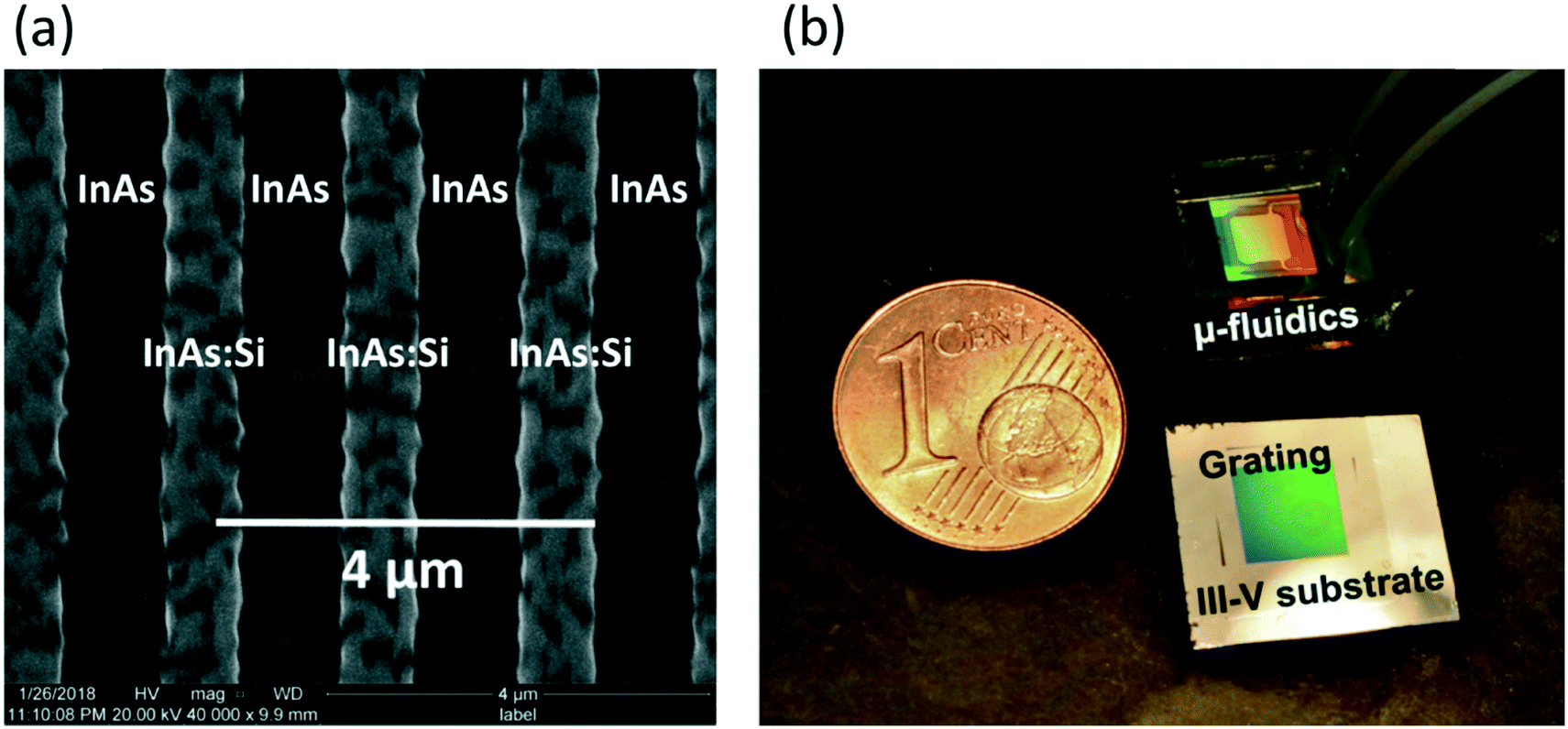 | ||
| Fig. 2 (a) Scanning electron microscopy (SEM) image of a III–V semiconductor plasmonic grating based on heavily Si-doped InAs ribbons on top of a III–V semiconductor substrate, here non-doped InAs. (b) Photography of a successful assembly of a III–V semiconductor mid-IR plasmonic grating and PDMS based microfluidic system for IR-spectroscopy in backside reflection configuration. The 1 cent euro coin with diameter of 16.25 mm illustrates the size of the system. | ||
Another way of combining semiconductor plasmonic system and polymer-based microfluidics for microscopic IR-spectroscopy applications is the so-called transmission configuration where the IR-opacity of the polymer used to define the microfluidic circuit is bypassed by inserting an IR-transparent window layer above the liquid measurement chamber. In the fabrication process, the IR-absorbing polymer is removed from the IR-beam path. The function of the IR-transparent window layer is two-fold as it should let IR-light pass, but at the same time seal the microfluidic circuit to avoid liquid leakage. Germanium was chosen in this work as IR-transparent window, because Ge has 47% transmission at 5 μm and the value decreases continuously to 30% transmission at 20 μm. The fabrication steps to insert a germanium window substrate into the microfluidic device are shown in Fig. 3. The process steps for the transmission configuration are similar to the process steps for the backside configuration. From the sketch of the beam path, shown in red in Fig. 3(c), the advantages of this design become clear. The improvement is that IR-light transmitted through the whole structure (InAs-substrate, liquid, Ge-window) can be collected and analysed by a microscopic IR-spectrometer operating in transmission mode while the same device can be operated as well in backside reflection mode.
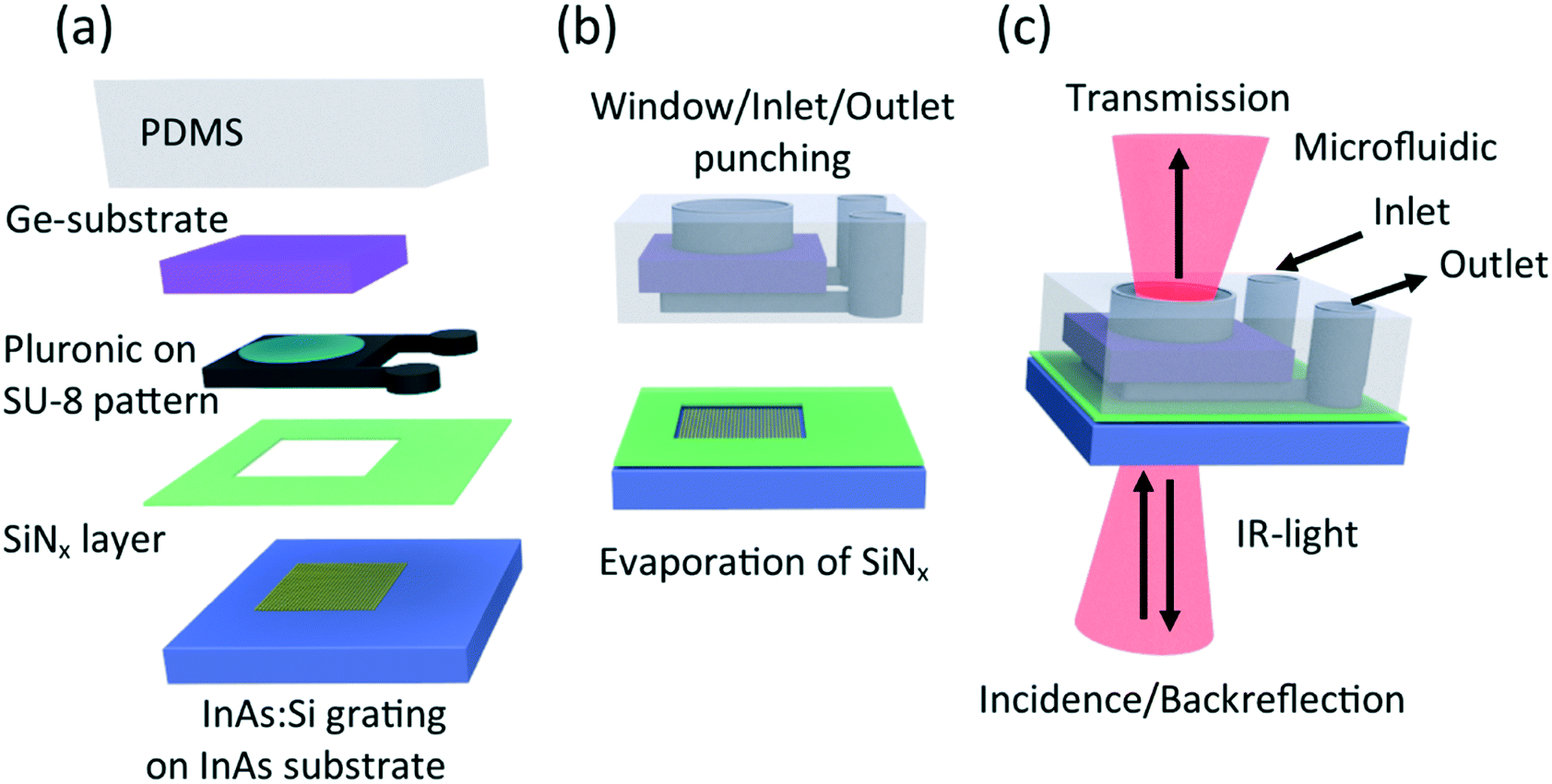 | ||
| Fig. 3 Instruction for assembling a semiconductor plasmonics system with a soft lithography (PDMS) produced microfluidic system for backreflection and transmission IR-spectroscopy. (a) The lithographically produced SU-8 pattern defines the PDMS casting mould. A small drop of liquid (cold) Pluronic is spread on the SU-8 at the position of the later measurement chamber and fixes a Ge-substrate when the Pluronic solidifies at room temperature. The SiNx layer evaporated onto the III–V semiconductor layer has an opening due to shadow masking at position of the plasmonic resonators. (b) Before the elastomeric PDMS is stripped from the SU-8, a punch removes the PDMS above the embedded Ge-substrate (window punching). Then, the sample was cooled down to liquefy the Pluronic and to facilitate the detachment. After stripping the PDMS with the embedded Ge-substrate from the SU-8, additional inlet and outlet channels are punched into the PDMS layer. (c) The final assembling steps consists in combining the PDMS layer with the SiNx layer after both contact surfaces were plasma activated to create bond forming surface radicals. The infrared beam path where the IR-light is incident and back-reflected through the backside of the InAs substrate is shown for illustration. The IR-light transmitted through the measurement chamber and through the Ge-substrate serving as topside IR-window layer is equally shown. | ||
As the process steps are similar to the process steps shown in Fig. 1, the focus here is on the additional technological steps. Fig. 3(a) shows the assembly of a microfluidic device in transmission configuration. The specific step here is to maintain the Ge window on top of the SU-8 pattern while uncured PDMS is poured on the silicon wafer. To do so we used a phase change polymer, namely poloxamer or Pluronic F127. This block copolymer shows a phase transition at 7 °C, being liquid below and gel over this temperature. A drop of liquid Pluronic F127 is then poured on the surface of the main chamber of the circuit. A 200 μm thick double side polished germanium wafer has been cut to 5 × 5 mm2 pieces using a Disco DAD3200 blade dicer. Then a piece of Ge is positioned on top of the SU-8 surface covered with Pluronic. A gentle pressure is applied to both align the Ge-substrate on top of the SU-8 chamber and to wet the surface between Ge-substrate and SU-8 chamber. When room temperature is reached, then the Pluronic solidifies to a paste which fixes the Ge-substrate in position. Furthermore, the Pluronic serves as buffer layer between SU-8 and germanium during the PDMS-casting. The casting of PDMS was followed by a low pressure treatment to evacuate air bubbles and followed by a baking step (70 °C, two hours) to cure the PDMS. Before unmolding of the PDMS from the substrate, the device was cooled down in a fridge to liquefy the Pluronic again and ease the unmolding process. Subsequently the PDMS was thoroughly rinsed with water to remove the Pluronic. Additional to the punching of inlet and outlet channels, an opening with 3 mm diameter and therefore smaller than the dimensions of the Ge-substrate was punched into the PDMS as can be seen in Fig. 3(b). This punch removed the PDMS, but left the germanium intact. Thus IR-measurement under flow and in transmission mode become possible. The other technological process steps were as previously described. It can be summarized that the additional process steps for assembling the semiconductor plasmonics system with a soft lithography (PDMS) produced microfluidic system, shown in Fig. 3, lead to working microfluidic devices for transmission and back-reflection IR-spectroscopy applications.
IR-spectroscopy in backside reflection configuration
After successful fabrication, the microfluidic device for surface-enhanced IR-spectroscopy in backside reflection configuration was tested. A microfluidic flow control system (Elveflow Microfluidic Pressure controller OB1 MK3) was used to work under reproducible flow conditions. The pumping pressure was set to obtain a flow rate of 0.033 ml min−1. For the first tests, water and ethanol were chosen as solvents. The choice of these liquids was motivated by the expectation of negligible chemical reactions with PDMS, InAs, InAs:Si and Ge. The swelling of PDMS upon ethanol contact was anticipated.43 Brukers Hyperion 3000 IR-microscope with Vertex 70 Fourier-transform infrared spectrometer (FTIR) was used. The microfluidic device was fixed on the sample holder and the microscope objectives were adjusted such that the focal plane was in the plane of the semiconductor plasmonic resonators. A polariser in the beam path orients the electric field of the IR-light parallel or perpendicular to the grating. The reference spectrum to determine the reflectance of the device is obtained on a gold mirror.The result of this IR-back-reflection study is shown in Fig. 4. The beam path is sketched in the inset of Fig. 4(a). In the top panel of Fig. 4(a), the IR-back-reflected light polarized perpendicular to the grating R⊥ is shown for ethanol flow (red line) and for water flow (blue line). For both solvents, a broad dip around 700 cm−1 (12 μm to 20 μm) can be seen in the spectra. Additionally, in the ethanol spectra, the C–O stretching modes can be seen as antisymmetric peaks in the 1050 to 1200 cm−1 region and a weak carbon–carbon (C–C) vibrational mode is detectable as antisymmetric peak centred around 880 cm−1. In the middle panel of Fig. 4(a), the IR-back-reflected light polarized parallel to the grating R∥ is shown for the flow of the two solvents. While the antisymmetric peaks, attributable to IR-vibrational modes of ethanol, are clearly visible, the broad dip around 700 cm−1 cannot longer be seen in the spectra. In the bottom panel of Fig. 4(a), the ratio R∥/R⊥ is shown. The antisymmetric peaks, attributed to C–C and C–O vibrational modes, cancel out and the broad signature around 700 cm−1 can be clearly seen as peak. The ethanol (red) and the water (blue) lines overlap from 1000 cm−1 to 1500 cm−1, but they are shifted one towards the other in the spectral region around 700 cm−1. The maxima of the water and the ethanol peak are shifted by 30 ± 5 cm−1. The broad R∥/R⊥ peak is attributed to the localized surface plasmon resonance (LSPR) of the nanoresonators and the LSPR-shift is explained by the difference of the refractive index of ethanol and water in this spectral range.44 As ethanol and water both have complex refractive indices in the range of interest, an analysis based on projection could be performed.45 This is nevertheless beyond the scope of this work and an open challenge for semiconductor surface plasmon resonance system working in the IR-range. It has to be noted that the antisymmetric peak shape of the IR-absorption modes originates from an interaction with the plasmonic resonators and can be described as Fano-like resonance.46
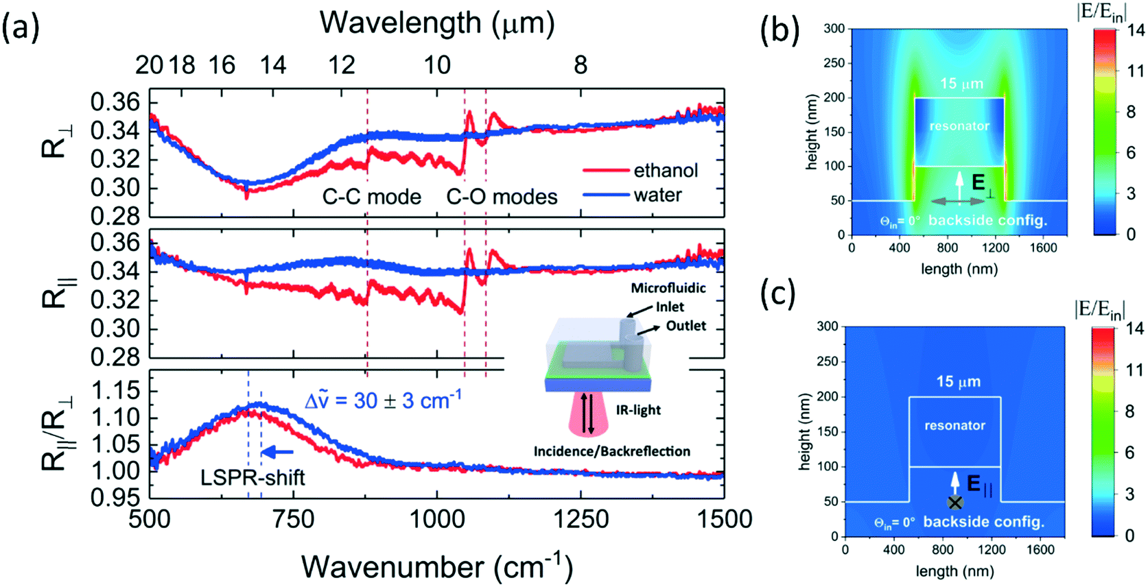 | ||
| Fig. 4 (a) Microscopic infrared spectroscopy in backside reflection configuration (sketched in the inset) was performed with the μ-fluidic sensor system shown in Fig. 2. Different spectral responses were obtained in dependence of the solvents in the microfluidic measurement chamber, either ethanol or water, and in dependence of the polarization of the incident and back-reflected light, either polarized perpendicular R⊥ or parallel R∥ to the grating. A localized surface plasmon resonance (LSPR) shift was observed for ethanol and water filling. (b) As the grating consists of many resonators, one resonator with adequate periodic boundary conditions was chosen for calculating the electric near-field at the resonance wavelength of 15 μm for polarization in-plane, i.e. perpendicular to the grating. The colour scale bar shows the electric field enhancement |E/Ein|. (c) The same resonator, at the same wavelength, but with light polarization out-of-plane, i.e. parallel to the grating, shows no near-field enhancement effect as the LSPR mode is not excited in this illumination condition. | ||
To underline the plasmonic nature of the observable peak, numerical finite-difference time domain (FDTD) calculations were performed with the commercially available software Lumerical FDTD solutions.47 In Fig. 4(b) and in Fig. 4(c), the calculated electric near-field enhancement |E/Ein| for one resonator, with adequately chosen periodic boundary conditions on the left and right side of the unit cell, is shown for the resonance wavelength of 15 μm. The length of the unit cell corresponds to the grating period and out-of-plane dimension, i.e. the third dimension is assumed to be infinite. The geometrical parameters of the model were chosen such that they correspond to the experimentally determined values. The refractive index for the plasmonic heavily Si-doped InAs layer was determined by Brewster mode measurements and subsequent fitting with a Drude function.48 In Fig. 4(b), the more than ten-fold enhancement of the local electric field E in terms of the incident electric field Ein decays rapidly away from the surface of the resonators' surface when exited with IR-light polarized perpendicular to the grating. The model focuses on the resonators' interface and light propagation through the InAs-substrate, such as light in-coupling from air into the InAs-substrate is neglected. The main conclusion is that the LSPR mode, exited at around 15 μm, leads to electric field enhancement which can be exploited for surface-enhanced infrared spectroscopy. In Fig. 4(c), the simulation result for incident IR-light polarized parallel to the grating is shown. It can be seen that no near-field enhancement is observable because the incident light is not confined within the resonator, therefore there is no LSPR excitation.
To summarize, the experiments and the supporting simulations demonstrate that microfluidic surface-enhanced infrared spectroscopy is possible in the backside reflection configuration when semiconductor plasmonic resonators are combined with soft lithography (PDMS) based microfluidic systems.
IR-spectroscopy in transmission configuration
Following the assembly instructions summarized in Fig. 3, a working device for IR-spectroscopy under flow conditions and in transmission configuration was fabricated and characterized. In a first step, the transmission through a non-doped InAs-substrate and through the semiconductor resonator system before combination with the microfluidic system was measured. The substrate was placed onto the sample stage of a Hyperion 3000 microscope. The focal plane was adjusted with the microscope's top and bottom objectives to obtain maximum transmission. To normalize the obtained spectrum, a spectrum without sample, i.e. 100% transmission was measured. Subsequently, the semiconductor resonator system with the integrated Ge-window was measured in transmission mode by choosing the focal plane to obtain maximum transmission. Then, the microfluidic flow control system was connected and transmission was measured for ethanol and water flow in the microfluidic measurement chamber. A polariser in the beam path allowed to choose IR-light polarisation parallel or perpendicular to the grating.The result of this IR-transmission study is shown in Fig. 5. In the top panel of Fig. 5(a), the IR-transmitted light polarized parallel to the grating T∥ and perpendicular to the grating T⊥ is shown. It can be seen that the InAs-substrate has good and nearly constant transmittance properties in the wavelength range from 4 μm to 8 μm. The measured value of 50% of transmittance is due to the relatively high refractive index of InAs (nInAs ≈ 3.4) which causes significant reflection losses at the air–InAs interface and can be easily improved by an anti-reflective coating for InAs. It should be noted that for both polarisations a decreasing transmittance is observed in the range from 8 μm to 20 μm. At 20 μm only 25% of the incident light is transmitted and this decrease of transmittance with higher wavelength is explained by multi-phonon absorption in the InAs-substrate.49 The significant spectral signature for sensing application is the transmission dip around 700 cm−1 (12 μm to 20 μm) appearing only for polarization perpendicular to the grating. This signature is attributed to a localized surface plasmon resonance. While this result is encouraging to pursue with the transmission configuration for surface-enhanced infrared absorption (SEIRA) spectroscopy, the middle panel of Fig. 5(a) shows that the plasmonic resonance is less visible in transmission configuration after combining the semiconductor plasmonic resonators with the Ge-window integrated microfluidic system. The main reason for blurring the detectability of the plasmonic signature is the appearance of interference due to light trapping within the air-filled measurement chamber. The overall transmittance is reduced as the IR-light has to be transmitted as well through the Ge-window. The transmittance values for light polarized parallel or perpendicular, plotted in red and black, were nearly indistinguishable. Instead of modelling all interfaces and explaining the observable interferences, a much simpler fit function with two free parameters accounting for InAs multi-phonon absorption at decreasing wavenumber was used to fit the measured data in the relevant wavenumber ![[small nu, Greek, tilde]](https://www.rsc.org/images/entities/char_e0e1.gif) range. This fit function is plotted in blue and the following formula was used:
range. This fit function is plotted in blue and the following formula was used:
Tfit,1 = 0.32–120 [cm−1]/![[small nu, Greek, tilde]](https://www.rsc.org/images/entities/i_char_e0e1.gif) [cm−1]. [cm−1]. |
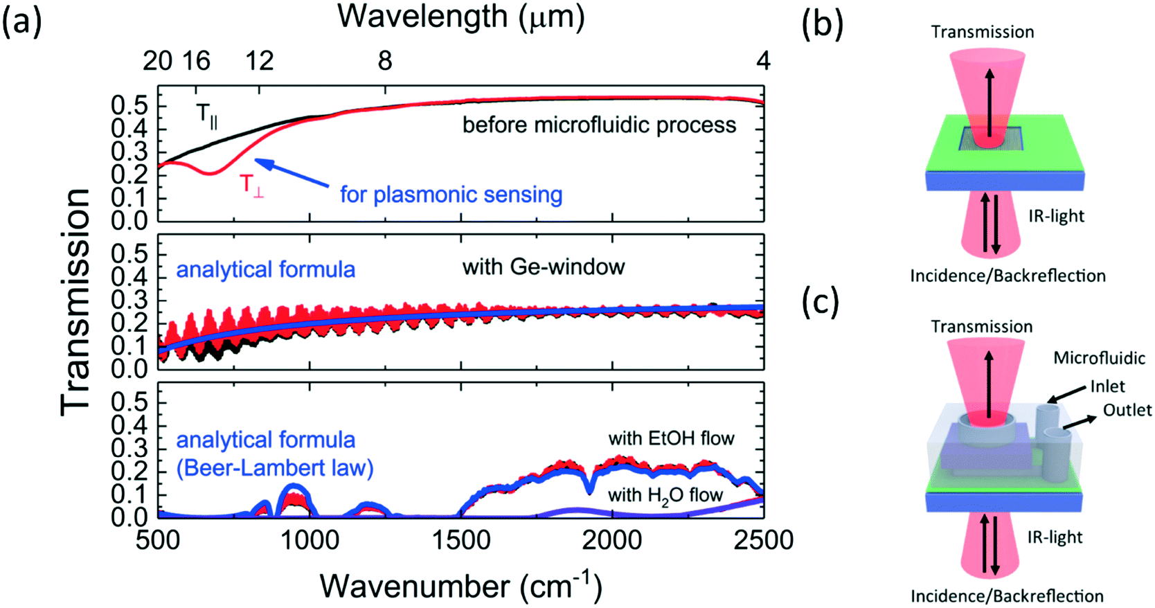 | ||
| Fig. 5 (a) Microscopic infrared spectroscopy in transmission configuration for the devices sketched in (b) and (c) is shown. Different spectral responses were obtained in dependence on the solvents in the microfluidic measurement chamber, either ethanol (EtOH) or water (H2O), and in dependence on the polarization of the incident and transmitted light, either polarized perpendicular T⊥ or parallel T∥ to the grating. The transmission through the InAs substrate and the plasmonic grating, sketched in (b), is shown in the top panel of (a). The transmission is decreasing with decreasing wavenumber and a plasmonic resonance leads to a T⊥ transmission dip for light polarized perpendicular to the grating. The transmission through the assembled μ-fluidic sensor, i.e. with Ge-window in the light beam path, is sketched in (c) and the measurement result is shown in the middle panel of (a). Interference effects and decreased transmission are observable. The trend of decreasing transmission with decreasing wavenumber is fitted by an analytical formula shown in blue. In the bottom panel of (a) the transmission for EtOH or H2O flow is shown. As EtOH and H2O have different, well-known IR-absorption characteristics, a fit of the reduced transmission is shown by considering the Beer–Lambert law (blue for EtOH flow and purple for H2O flow). | ||
When the measurement chamber was filled with ethanol or water via the microfluidic flow control system, then the transmittance was another time strongly modified as can be seen in the bottom panel of Fig. 5(a). The transmittance of water and ethanol for both light-polarizations does not demonstrate any difference. However, a clear difference depending on the inserted solvent can be seen. While water lets no IR-light pass, except for two small transmission zone around 1800 cm−1 and around 2500 cm−1, the ethanol filling leads to relatively good transmission window between 1500 cm−1 to 2500 cm−1 and three smaller ones around 1000 cm−1. The disappearance of the interference and the strong reduction of transmission due to the liquid filling can be easily understood by the absorptive nature of the chosen solvents. Besides distinguished IR-absorption signatures, both liquids have a non-negligible IR-absorption baseline. In blue, both spectra were plotted by a fit function with includes the Beer–Lambert law:
As the extinction coefficient κ as imaginary part of the refractive index is well known for water and ethanol,44 the fitting allows to determine a value for the thickness t of the measurement chamber. The found value of 84 ± 10 μm is in the same order as the height of the SU-8 used to define the chamber. This demonstrates that the Pluronic fabrication step did not substantially increase the height. More importantly, the results clearly show that the microfluidic device is working in transmission configuration, but this configuration is not suited for surface-enhanced infrared spectroscopy as absorption in the micro-metric fluidic chamber dominates the transmission spectra. Ultra-thin microfluidic detection chambers might be a way to allow SEIRA spectroscopy in the transmission configuration. Additionally, the transmission could be increased and the inference fringes reduced by adding anti-reflective coatings.
Demonstration of alcohol sensing capacity
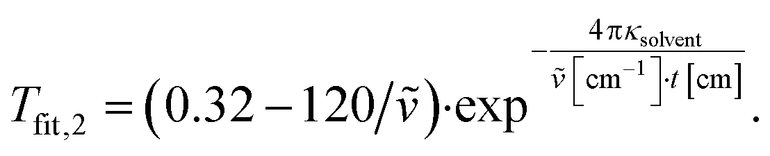
Having fabricated and tested firstly the device for backside reflection operation and then the device for transmission and backside reflection operation, the advantages of the backside reflection configuration for surface-enhanced IR-sensing became clear and will be further elaborated in the following. As 100% of water flow and 100% of ethanol flow was already tested and explained in the section on IR-spectroscopy in backside reflection configuration, the focus of this section is a detailed investigation of ethanol–water mixtures. Although volume ratios are more intuitive to obtain in a chemistry lab, the choice was made to investigate molar ratios. The main advantage of using molar ratios is the possibility to correlate the IR-absorption intensity with the amount of absorbing molecules. Five different solutions of different ethanol–water mixtures were prepared and one after the other inserted via the flow controller into the measurement chamber. A sufficient waiting time of 5 min in between measurements allowed the new liquid to replace the liquid from the previous measurement in the microfluidic device. Additional to the waiting time necessary to replace the liquid flow in the measurement chamber, it was necessary to wait for PDMS de-swelling when the polymer was no longer in contact with ethanol. Over time, the ambient measurement conditions are changing. Therefore, it is necessary to minimize the time between background reference measurement, i.e. gold mirror reflection measurement, and backside-reflection measurements with different solvents in the liquid chamber. In Fig. 6(a) the results of this experimental series are summarized. Constant off-set values were added to show 10 spectra in one graph. On top, in blue, 100% of ethanol flow is shown for polarization parallel and perpendicular to the grating. The localized surface plasmon resonance (LSPR) can be seen around 15 μm for light polarized perpendicular to the grating. Independent from the chosen polarization, the C–C and C–O vibrational modes of ethanol can be seen as anti-symmetric signatures in the spectra. From the top to the bottom of Fig. 6(a), the alcohol content is decreased and the IR signatures representative for ethanol decrease in intensity when the water content is increased in the measurement chamber. The differences between R∥ and R⊥ for the water flow measurements at higher wavenumbers shown in Fig. 6(a) are probably a measurement artefact and could be explained by an insufficient waiting time to account for PDMS de-swelling. The measurement data was analysed and the result is shown in Fig. 6(b). The x-axis shows the molar ratio of ethanol in water. The red and black curves correspond to the difference of maximum and minimum values (max–min) taken for the first derivative of the determined reflectance around an IR-vibrational mode (left y-axis). The main advantage of this data treatment was that the values could be read out much easier and without over- or underestimation of the value due to the observable noise. The red curve shows the C–O stretching mode at 1055 cm−1 and the black curve shows the C–C stretching mode at 880 cm−1. Both curves increase with the ethanol content and can serve as a calibration curve for alcoholic beverage. The right y-axis corresponds to the blue curve labelled LSPRmax and the corresponding unit is wavenumber. To determine the wavenumber corresponding to the maximum of the localized plasmon resonance (LSPR), the R∥/R⊥ peaks were fitted by a Lorentz fit function and the location parameter of the fit function was determined as LSPRmax wavenumber. It can be clearly seen that the LSPRmax wavenumber is decreasing with increasing ethanol content. This is attributed to the modified refractive index of the resonators' optical environment. This demonstrates that the device does not only allow IR-spectroscopy to measure IR-modes of liquids but also surface plasmon resonance (SPR) sensing in the infrared range. Due to the complex refractive indices of ethanol and water in the investigated IR-range, a simple determination of the refractive index sensitivity is not possible, but a more complete analysis based on projection could be performed in the future.45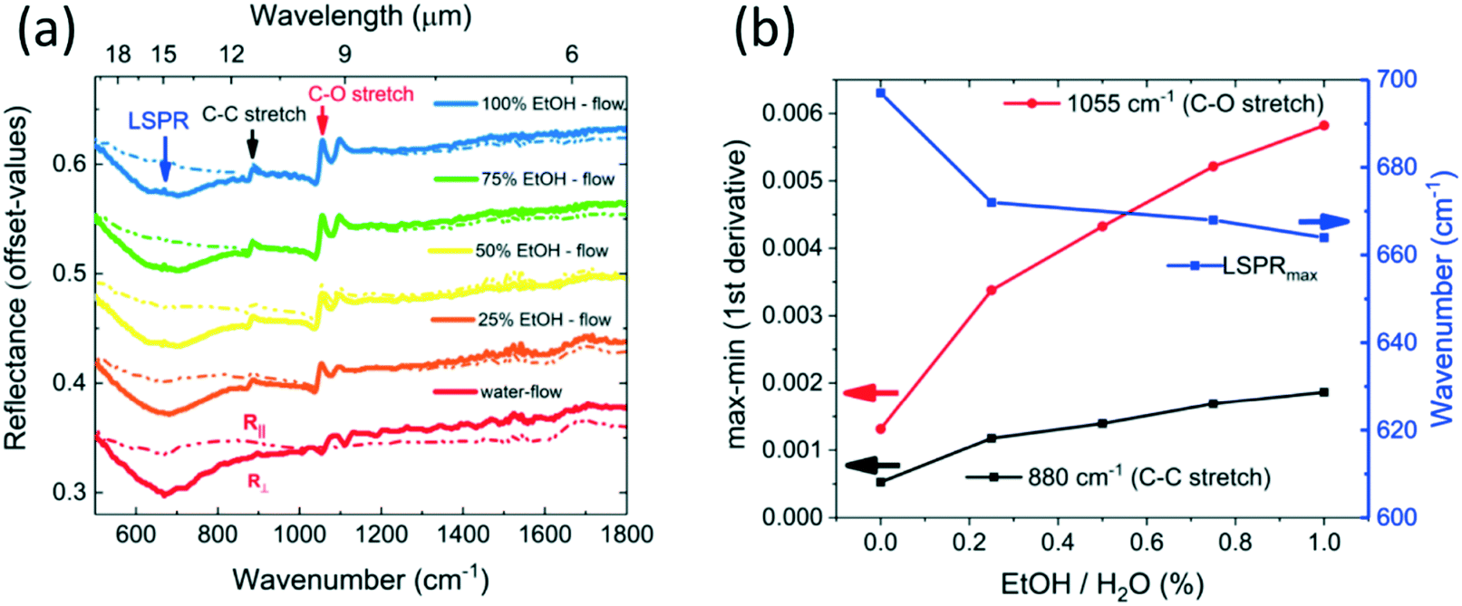 | ||
| Fig. 6 (a) The μ-fluidic sensor system shown in Fig. 2 was used for microscopic infrared spectroscopy in backside reflection configuration for different molar concentrations of EtOH in water. The localized surface plasmon resonance (LSPR) appears as dip in the reflectance curve for incident light polarized perpendicular to the grating R⊥ (solid lines) and not for light polarized parallel to the grating R∥ (dashed lines). In both polarizations the C–C stretching mode and the C–O stretching mode of EtOH can be seen as Fano-like resonances. Under pure water flow, these EtOH IR-signatures vanish. (b) The x-axis shows the molar percentage of EtOH in water. The left y-axis shows the differences in reflectance, i.e. the maximum–minimum values of the first derivative around the IR-absorption signature, for the C–C and the C–O stretching mode. The right y-axis shows a wavenumber scale. As the ratio of R∥/R⊥ leads to a peak, a fit of this peak allows to extract the wavenumber where the LSPR resonance is maximum. A decrease of the LSPRmax wavenumber with increasing EtOH molecules can be observed. | ||
Demonstration of the capacity to monitor surface reactions
To further elaborate on the surface plasmon resonance (SPR) sensing capacity and to indicate possibilities and limitations of this semiconductor sensing device for surface-enhanced infrared spectroscopy, the impact of the formation of a self-assembled monolayer (SAM) on the IR-spectra was investigated in the backside configuration. Commercially available molecules with phenyl-terminal group bonded via a carbon chain to a phosphonic acid (PA) anchor group, subsequently called Phenyl10PA, were dissolved in pure ethanol. The 10-phenyldecylphosphonic acid (cas no. 1429741-23-0) was synthesized by Sikemia (Montpellier, France) and diluted in pure ethanol (API, >99%) to obtain a 1 mM solution. The choice of this molecule to study surface reactions on III–V semiconductor surfaces, such as the exposed InAs-substrate surface and the exposed InAs:Si resonator surface, is motivated by a recently published work where successful adsorption of the same phosphonic acid anchor group on GaSb and InAsSb surfaces was demonstrated.50 It could be demonstrated that the adsorption and the reaction with surface oxides lead to phosphonate monolayer formation. Additionally, the molecule with its one-side terminated phosphonic acid group is not expected to form multilayers when dissolved in pure ethanol.51 The procedure of this surface reaction experiment consists in three steps. At first, the liquid chamber was filled with pure ethanol via the microfluidic flow controller. Reference spectra were taken. Secondly, the ethanol vial was replaced by a vial filled with 1 mM Phenyl10PA in ethanol and the start of the reaction was the entry of the liquid into the measurement chamber via the flow controller. The reaction could be monitored by taking regular IR-measurements. In the end, after 13 h of 1 mM Phenyl10PA dissolved in ethanol flowing through the measurement chamber, the device was rinsed by pure ethanol flow for more than 10 minutes. The IR back-reflection spectra taken in 100% ethanol environment, after the reaction of the exposed surface to Phenyl10PA, allow a before/after comparison. The result of this experiment is shown in Fig. 7. In the inset of Fig. 7, a sketch of the Phenyl10PA molecule can be seen. The black curve corresponds to the R∥/R⊥ values before the surface reaction and the red curve corresponds to the measurement results after the surface was exposed to the Phenyl10PA dissolved in ethanol. It can be seen that after the reaction the resonance peak is red-shifted by 6 ± 1 cm−1 (140 ± 23 nm). As the resonance peak can be attributed to a localized surface plasmon resonance (LSPR), and it is well known that a minute variation of the optical environment of a LSPR-sensing system, such as the formation of a self-assembled monolayer on the plasmonic resonator surface, causes a detectable LSPR-shift, we interpret the observable shift as an indicator of a surface reaction. As the potentially complex refractive index of the investigated molecule is not known, a detailed analysis of the SPR-shift is beyond the scope of this work. It can be concluded that the fabricated device allows to measure surface reactions involving small molecular quantities in the flow-regime when operated in the backside reflection configuration. | ||
| Fig. 7 The ratio of R∥ to R⊥ before (black curve) and after (red curve) the resonators were exposed for 13 h to a microfluidic flow of 1 mM Phenyl10PA in EtOH solution is shown. Despite long rinsing with 100% EtOH, after the exposure to the phosphonic acid solution, the original LSPR was not recovered and a clear red-shift of the LSPR peak is observable. | ||
Conclusion
This works shows that semiconductor infrared plasmonic resonators can be combined with soft lithography (PDMS) produced microfluidic systems. This combination allows surface-enhanced infrared spectroscopy of molecules in the flow regime. By testing two different designs, it was found that the backside configuration is superior for surface-enhanced infrared spectroscopy due to the advantage that the surface plasmon resonance can be read-out easily. The tested transmission configuration led to a working microfluidic device, but IR-transmission through the 84 μm thick liquid chamber was dominated by liquid IR-absorption and is therefore not suitable to detect changes of the systems surface plasmon resonance. The advantageous backside configuration was exploited for sensing applications. It was shown that the semiconductor plasmonic microfluidic device allows to measure in a quantitative way the alcohol content of a steady flow of liquids and at the same time a plasmonic resonance shift due to the modification of the optical environment of the plasmonic resonator. In particular, the surface-sensitive shift of the surface plasmon resonance was used to demonstrate that the device has the potential to measure surface reactions involving small molecular quantities such as the formation of a self-assembled monolayer in the flow-regime. This semiconductor approach is particularly interesting as IR-sources, IR-detectors, and IR-resonators can potentially be integrated on-chip.Materials and methods
MBE growth and nanostructuration
A RIBER 412 molecular beam epitaxy (MBE) system was used to grow a 100 nm thin layer of heavily Si-doped InAs on a commercially available residually-doped InAs substrate from Wafer Technology. The plasmonic properties of the heavily doped layer were determined by measuring the mid-IR Brewster mode and subsequent fitting with Drude functions.48 We assume a continuous doping gradient, but a good agreement between experimental and simulation result were obtained in the mid-IR range by dividing the 100 nm InAs:Si layer into two parts. First, a 50 nm thick higher doped layer described by ε∞ = 12.3, ωp = 1.15 × 10¹⁵ rad s−1, γp = 2.8 × 10¹³ rad s−1 and then a second 50 nm thick layer with lower doping level described by ε∞ = 12.3, ωp = 0.98 × 10¹⁵ rad s−1, γp = 2.5 × 10¹³ rad s−1. The nanofabrication process based on photolithography follows recipes reported in previous work on the fabrication of III–V plasmonic nanoresonators.20,41,52 The grating fabricated for this work was characterized by a Nanoscope IV atomic force microscope (AFM) with a cantilever (PPP-NCH-10, Nanosensors). A ribbon height of 150 ± 20 nm and a grating periodicity of 1800 ± 20 nm were determined. A Fei Inspect S-50 scanning electron microscope (SEM) allowed to confirm the grating periodicity and to determine a grating width of 750 ± 20 nm. These parameters were used for finite difference time domain (FDTD) modelling with Lumerical FDTD solutions.47Microfluidic fabrication
The fabrication of the polydimethylsiloxane (PDMS) microfluidic system follows established process steps.6,7 It starts with the spin-coating of a 80 μm thick layer of SU-8 2100 on a 3 inch silicon wafer. The measurement chamber has a width of 3 mm and a length of 3 mm. Baking, UV exposure and developing define the microfluidic channels. A 10![[thin space (1/6-em)]](https://www.rsc.org/images/entities/char_2009.gif) :1 mix of silicone elastomer and its curing agent (Sylgard 184, Dow Corning) was cast onto the SU-8 motif. Air bubbles were removed by a low-quality vacuum for 1 h and then PDMS polymerization was achieved at 70 ° C for 2 h in an oven. The PDMS microfluidic system was then stripped off the SU-8 and two 0.6 mm wide inlet and outlet channels were punched into the PDMS.
:1 mix of silicone elastomer and its curing agent (Sylgard 184, Dow Corning) was cast onto the SU-8 motif. Air bubbles were removed by a low-quality vacuum for 1 h and then PDMS polymerization was achieved at 70 ° C for 2 h in an oven. The PDMS microfluidic system was then stripped off the SU-8 and two 0.6 mm wide inlet and outlet channels were punched into the PDMS.
SiNx evaporation, plasma activation, and bonding
Before bonding with the polydimethylsiloxane (PDMS) microfluidic system, a 200 nm thin SiNx-layer was deposited by plasma enhanced chemical vapor deposition (PECVD, Corial D250, CORIAL S.A, France) on top of the InAs-substrate while the 4 × 4 mm2 grating area was shadowed by a 5 × 5 mm2 piece cleaved from a germanium wafer. The PDMS microfluidic system and the InAs-substrate with SiNx-layer and uncovered grating structure were cleaned with ethanol and rinsed with distilled water. Then they were placed in a plasma cleaner (Femto low-pressure plasma system, Diener electronic GmbH, Germany) for 60 s for surface activation. After connecting the activated PDMS and SiNx-surface, the assembled device was cured for 5 min at 110 °C on a hot plate.IR-spectroscopy
The infrared spectra were measured with a Hyperion 3000 IR-microscope coupled to a Vertex 70 Fourier-transform infrared (FT-IR) spectrometer from Bruker. The light originating from a globar source was focused onto the sample with a ×15 magnification Cassegrain objective (NA = 0.4). A polarizer in the beam path enabled polarization dependent detection of the reflection signal with a single element liquid nitrogen cooled mercury cadmium telluride detector. In the transmission configuration, a second ×15 objective could be adjusted to set the focal plane of both objectives to the plane of the plasmonic resonators. The FT-IR was set to take per spectrum of 200 scans with 2 cm−1 resolution.Funding
French Investment for the Future program (EquipEx EXTRA, ANR 11-EQPX-0016); French ANR (SUPREME-B, ANR-14-CE26-0015); European Union's Horizon 2020 research and innovation programme (Marie Sklodowska-Curie grant agreement no. 641899); Occitanie region.Conflicts of interest
There are no conflicts to declare.Acknowledgements
J.-M. Peiris, J. Lyonnet and F. Pichot are acknowledged for technical support at the cleanroom facilities of the Université de Montpellier. G. Boissier, J.-M. Aniel and G. Narcy are acknowledged for technical support.References
- A. Perro, G. Lebourdon, S. Henry, S. Lecomte, L. Servant and S. Marre, Combining microfluidics and FT-IR spectroscopy: towards spatially resolved information on chemical processes, React. Chem. Eng., 2016, 1(6), 577–594 RSC.
- P. Sagmeister, J. D. Williams, C. A. Hone and C. O. Kappe, Laboratory of the future: a modular flow platform with multiple integrated PAT tools for multistep reactions, React. Chem. Eng., 2019, 4(9), 1571–1578 RSC.
- P. Yager, T. Edwards, E. Fu, K. Helton, K. Nelson and M. R. Tam, et al., Microfluidic diagnostic technologies for global public health, Nature, 2006, 442(7101), 412–418 CrossRef CAS PubMed.
- D. Gallegos, K. D. Long, H. Yu, P. P. Clark, Y. Lin and S. George, et al., Label-free biodetection using a smartphone, Lab Chip, 2013, 13(11), 2124–2132 RSC.
- J. Homola, Surface Plasmon Resonance Based Sensors, Springer Berlin Heidelberg, 2006 Search PubMed.
- P. Tabeling, Introduction to microfluidics, Oxford University Press, Oxford, U.K., New York, 2005, p. 301 Search PubMed.
- D. E. Angelescu, Highly Integrated Microfluidics Design, Artech House, 2011 Search PubMed.
- A. Z. Subramanian, E. Ryckeboer, A. Dhakal, F. Peyskens, A. Malik and B. Kuyken, et al., Silicon and silicon nitride photonic circuits for spectroscopic sensing on-a-chip [Invited], Photonics Res., 2015, 3(5), B47 CrossRef CAS.
- R. Aroca, Surface-enhanced vibrational spectroscopy, Wiley, Hoboken, NJ, 2006, p. 233 Search PubMed.
- Surface-Enhanced Raman Scattering: Physics and Applications, ed. K. Kneipp, M. Moskovits and H. Kneipp, Topics in applied physics, Springer, Berlin, New York, 2006, ISBN 978-3-540-33566-5 Search PubMed.
- R. Gao, N. Choi, S.-I. Chang, S. H. Kang, J. M. Song and S. I. Cho, et al., Highly sensitive trace analysis of paraquat using a surface-enhanced Raman scattering microdroplet sensor, Anal. Chim. Acta, 2010, 681(1–2), 87–91 CrossRef CAS.
- A. März, T. Henkel, D. Cialla, M. Schmitt and J. Popp, Droplet formation via flow-through microdevices in Raman and surface enhanced Raman spectroscopy—concepts and applications, Lab Chip, 2011, 11(21), 3584 RSC.
- Y. Wang, R. Vaidyanathan, M. J. A. Shiddiky and M. Trau, Enabling Rapid and Specific Surface-Enhanced Raman Scattering Immunoassay Using Nanoscaled Surface Shear Forces, ACS Nano, 2015, 9(6), 6354–6362 CrossRef CAS.
- F. Neubrech, C. Huck, K. Weber, A. Pucci and H. Giessen, Surface-Enhanced Infrared Spectroscopy Using Resonant Nanoantennas, Chem. Rev., 2017, 117(7), 5110–5145 CrossRef CAS.
- Y. Zhong, S. D. Malagari, T. Hamilton and D. Wasserman, Review of mid-infrared plasmonic materials, J. Nanophotonics, 2015, 9(1), 093791 CrossRef.
- F. B. Barho, F. Gonzalez-Posada, M.-J. Milla-Rodrigo, M. Bomers, L. Cerutti and T. Taliercio, All-semiconductor plasmonic gratings for biosensing applications in the mid-infrared spectral range, Opt. Express, 2016, 24(14), 16175 CrossRef CAS.
- A. S. Kuznetsov, Effect of Proximity in Arrays of Plasmonic Nanoantennas on Hot Spots Density: Degenerate Semiconductors vs, Conventional Metals, Plasmonics, 2016, 11(6), 1487–1493 CrossRef CAS.
- A. S. Kuznetsov, P. Schäfer, W. John, D. Prasai, S. Sadofev and S. Kalusniak, Enabling novel functionality in heavily doped ZnO:Ga by nanostructuring: an efficient plasmonic refractive index sensor, Nanotechnology, 2016, 27(2), 02LT CrossRef.
- L. Baldassarre, E. Sakat, J. Frigerio, A. Samarelli, K. Gallacher and E. Calandrini, et al., Midinfrared Plasmon-Enhanced Spectroscopy with Germanium Antennas on Silicon Substrates, Nano Lett., 2015, 15(11), 7225–7231 CrossRef CAS.
- F. Barho, F. Gonzalez-Posada and M. Milla, et al., Highly doped semiconductor plasmonic nanoantenna arrays for polarization selective broadband surface-enhanced infrared absorption spectroscopy of vanillin, Nanophotonics, 2017, 7(2), 507–516 Search PubMed.
- S. Law, L. Yu, A. Rosenberg and D. Wasserman, All-Semiconductor Plasmonic Nanoantennas for Infrared Sensing, Nano Lett., 2013, 13(9), 4569–4574 CrossRef CAS.
- S. A. Jewett, J. A. Yoder and A. Ivanisevic, Surface modifications on InAs decrease indium and arsenic leaching under physiological conditions, Appl. Surf. Sci., 2012, 261, 842–850 CrossRef CAS.
- M. Bomers, D. M. Di Paola, L. Cerutti, T. Michel, R. Arinero and E. Tournié, et al., Mid-IR plasmonic compound with gallium oxide toplayer formed by GaSb oxidation in water, Semicond. Sci. Technol., 2018, 33(9), 095009 CrossRef.
- Mid-Infrared Semiconductor Optoelectronics, ed. A. Krier, Springer series in optical sciences, Springer, London, 2006, ISBN 978-1-84628-208-9 Search PubMed.
- E. A. Plis, InAs/GaSb Type-II Superlattice Detectors, Adv. Electron., 2014, 2014, 1–12 CrossRef.
- W. Zhou, N. Bandyopadhyay, D. Wu, R. McClintock and M. Razeghi, Monolithically, widely tunable quantum cascade lasers based on a heterogeneous active region design, Sci. Rep., 2016, 6, 25213 CrossRef CAS.
- H. Nguyen-Van, A. N. Baranov, Z. Loghmari, L. Cerutti, J.-B. Rodriguez and J. Tournet, et al., Quantum cascade lasers grown on silicon, Sci. Rep., 2018, 8(1), 7206 CrossRef.
- T. Taliercio and P. Biagioni, Semiconductor infrared plasmonics, Nanophotonics, 2019, 8(6), 949–990 CAS.
- K. L. A. Chan, S. Gulati, J. B. Edel, A. J. de Mello and S. G. Kazarian, Chemical imaging of microfluidic flows using ATR-FTIR spectroscopy, Lab Chip, 2009, 9(20), 2909 RSC.
- S. G. Kazarian and K. L. A. Chan, ATR-FTIR spectroscopic imaging: recent advances and applications to biological systems, Analyst, 2013, 138(7), 1940 RSC.
- K. L. A. Chan, X. Niu, A. J. de Mello and S. G. Kazarian, Rapid prototyping of microfluidic devices for integrating with FT-IR spectroscopic imaging, Lab Chip, 2010, 10(16), 2170 RSC.
- K. L. A. Chan and S. G. Kazarian, FT-IR Spectroscopic Imaging of Reactions in Multiphase Flow in Microfluidic Channels, Anal. Chem., 2012, 84(9), 4052–4056 CrossRef CAS.
- S. G. Kazarian, Enhancing high-throughput technology and microfluidics with FTIR spectroscopic imaging, Anal. Bioanal. Chem., 2007, 388(3), 529–532 CrossRef CAS.
- K. Ataka, S. T. Stripp and J. Heberle, Surface-enhanced infrared absorption spectroscopy (SEIRAS) to probe monolayers of membrane proteins, Biochim. Biophys. Acta, Biomembr., 2013, 1828(10), 2283–2293 CrossRef CAS.
- O. Limaj, D. Etezadi, N. J. Wittenberg, D. Rodrigo, D. Yoo and S.-H. Oh, et al., Infrared Plasmonic Biosensor for Real-Time and Label-Free Monitoring of Lipid Membranes, Nano Lett., 2016, 16(2), 1502–1508 CrossRef CAS.
- R. Adato and H. Altug, In-situ ultra-sensitive infrared absorption spectroscopy of biomolecule interactions in real time with plasmonic nanoantennas, Nat. Commun., 2013, 4, 2154 CrossRef PubMed.
- T. H. H. Le and T. Tanaka, Plasmonics–Nanofluidics Hydrid Metamaterial: An Ultrasensitive Platform for Infrared Absorption Spectroscopy and Quantitative Measurement of Molecules, ACS Nano, 2017, 11(10), 9780–9788 CrossRef CAS.
- D. Rodrigo, A. Tittl, N. Ait-Bouziad, A. John-Herpin, O. Limaj and C. Kelly, et al., Resolving molecule-specific information in dynamic lipid membrane processes with multi-resonant infrared metasurfaces, Nat. Commun., 2018, 9(1), 2160 CrossRef PubMed.
- M. Sieger and B. Mizaikoff, Toward On-Chip Mid-Infrared Sensors, Anal. Chem., 2016, 88(11), 5562–5573 CrossRef CAS.
- Y.-C. Chang, P. Wägli, V. Paeder, A. Homsy, L. Hvozdara and P. van der Wal, et al., Cocaine detection by a mid-infrared waveguide integrated with a microfluidic chip, Lab Chip, 2012, 12(17), 3020–3023 RSC.
- M. J. Milla, F. Barho, F. González-Posada, L. Cerutti, M. Bomers and J. B. Rodriguez, et al., Localized surface plasmon resonance frequency tuning in highly doped InAsSb/GaSb one-dimensional nanostructures, Nanotechnology, 2016, 27(42), 425201 CrossRef CAS PubMed.
- S. Roux, L. Cerutti, E. Tournie, B. Gérard, G. Patriarche and A. Grisard, et al., Low-loss orientation-patterned GaSb waveguides for mid-infrared parametric conversion, Opt. Mater. Express, 2017, 7(8), 3011 CrossRef CAS.
- J. N. Lee, C. Park and G. M. Whitesides, Solvent Compatibility of Poly(dimethylsiloxane)-Based Microfluidic Devices, Anal. Chem., 2003, 75(23), 6544–6554 CrossRef CAS.
- E. Sani and A. Dell'Oro, Spectral optical constants of ethanol and isopropanol from ultraviolet to far infrared, Opt. Mater., 2016, 60, 137–141 CrossRef CAS.
- S. Filion-Côté, M. Tabrizian and A. G. Kirk, Real-time measurement of complex refractive indices with surface plasmon resonance, Sens. Actuators, B, 2017, 245, 747–752 CrossRef.
- B. Luk'yanchuk, N. I. Zheludev, S. A. Maier, N. J. Halas, P. Nordlander and H. Giessen, et al., The Fano resonance in plasmonic nanostructures and metamaterials, Nat. Mater., 2010, 9(9), 707–715 CrossRef PubMed.
- Lumerical Solutions I, 2017 Search PubMed.
- T. Taliercio, V. N. Guilengui, L. Cerutti, E. Tournié and J.-J. Greffet, Brewster “mode” in highly doped semiconductor layers: an all-optical technique to monitor doping concentration, Opt. Express, 2014, 22(20), 24294 CrossRef CAS.
- E. S. Koteles and W. R. Datars, Two-phonon absorption in InSb, InAs, and GaAs, Can. J. Phys., 1976, 54(16), 1676–1682 CrossRef CAS.
- M. Bomers, A. Mezy, L. Cerutti, F. Barho, F. Gonzalez-Posada Flores and E. Tournié, et al., Phosphonate monolayers on InAsSb and GaSb surfaces for mid-IR plasmonics, Appl. Surf. Sci., 2018, 451, 241–249 CrossRef CAS.
- G. Guerrero, J. G. Alauzun, M. Granier, D. Laurencin and P. H. Mutin, Phosphonate coupling molecules for the control of surface/interface properties and the synthesis of nanomaterials, Dalton Trans., 2013, 42(35), 12569 RSC.
- V. N'Tsame Guilengui, L. Cerutti, J. B. Rodriguez, E. Tournié and T. Taliercio, Localized surface plasmon resonances in highly doped semiconductors nanostructures, Appl. Phys. Lett., 2012, 101(16), 161113 CrossRef.
| This journal is © The Royal Society of Chemistry 2020 |