
 Open Access Article
 This Open Access Article is licensed under a Creative Commons Attribution-Non Commercial 3.0 Unported Licence
The density, nanohardness and some optical properties of As–S and As–Se chalcogenide bulk glasses and thin films†
P. Knotek b,
P. Kutálek*a,
E. Černoškováa,
M. Vlčeka and
L. Tichýb
b,
P. Kutálek*a,
E. Černoškováa,
M. Vlčeka and
L. Tichýb
aUniversity of Pardubice, Faculty of Chemical Technology, Joint Laboratory of Solid State Chemistry, Studentská 84, 532 10 Pardubice, Czech Republic. E-mail: petr.kutalek@upce.cz; Tel: +420 466036155
bUniversity of Pardubice, Faculty of Chemical Technology, Department of General and Inorganic Chemistry, Studentská 573, 532 10 Pardubice, Czech Republic
First published on 24th November 2020
Abstract
Amorphous As2S3, As2Se3 and As1Se99 bulk glasses and thin films were prepared by the melt quenching technique and vacuum thermal evaporation, respectively, on different substrates. The density (ρ) – determined by the simple and cheap method of precise weighting, refractive index (n), structural arrangement – inferred from Raman spectroscopy, and nanohardness (Hind) were determined for all the studied materials in both bulk and thin film states. It is found that regardless of the chemical composition, the bulk glass density, refractive index and nanohardness are higher in comparison with those of the corresponding virgin and by annealing relaxed thin films, and the observed differences are discussed. The almost negligible influence of the substrate on the thin films density, structural arrangement and nanohardness, was observed.
1. Introduction
Chalcogenide glasses and amorphous thin films possess some interesting properties such as a non-linear optical properties, high infrared transparency, high refractive index, photosensitivity etc. Therefore, they remain a key subject of study and find utilization in many promising applications such as an infrared technology, integrated and nonlinear optics, phase change memory, etc.1,2 Also the structural arrangement of chalcogenide glasses is still of interest.3–5One of the important mechanical characteristics of solids is density, which affects various optical, electrical and mechanical properties. Changes in density can significantly influence the refractive index of a material as it follows for example, from the Lorentz–Lorenz relation.6,7 For optical memories, that use inclusive phase change materials (PCM), the density changes indicate the possibility to reach a high optical contrast. On the contrary, the absence of density changes is preferred in the case of phase change random access memories (PCRAM), where density changes could lead to failure of a device due to stress between, for example, electrodes and PCM layers.8 In many amorphous chalcogenides the intrinsic photodarkening is associated with a change in the sample thickness, it means density changes, which reflect some photo induced structural changes in the material.9,10 Although the density of many materials in the bulk form is well known and easy to determine, this is not always the case for materials in a thin film form.
Some ways to determine thin film density have been reported in the literature. For example, the density of metallic films was obtained by Samuelsson et al. employing Rutherford backscattering spectrometry.11 Waseda et al.12 described the determination of molybdenum thin film density using a pressure-of-flotation method. The determination of the thin film density of amorphous germanium measured by an in situ and non-destructive method based on a quartz single-crystal oscillator, was described by Viščor et al.13 Another important non-destructive method is X-ray reflectivity measurement.14 For some other different approaches, including the Swanepoel method, see for example ref. 15–18.
The other mechanical property which is important not only for thin film applications, but also for improved understanding of the structure and other physical and chemical properties of thin films, is the nanoindentation hardness (nanohardness), developed as a depth-sensing indentation technique in 1983.19,20 The nanohardness of chalcogenide bulk glass and thin films are not frequently studied or even compared. Ge–Se chalcogenide bulk glasses were, for example, studied by Guin et al.21 from the point of hardness, toughness and scratchability. They discussed the hardness and fracture toughness as the result of structural models accounting for the topological changes occurring in a glass network. As2Se3 thin films with combined nanoindentation and AFM methods by Trunov et al.22 were investigated, and the authors used the multi-cycling test to probe the local photomechanical response of the thin films. Also Sabapathy et al.23 and Ding et al.24 studied nanoindentation in waveguides and thin films, respectively. The mechanical properties of chalcogenide glasses by Rajakumar et al.25 and Prabhudessai et al.26 were studied, however, from the point of Vicker’s hardness.
In the present paper, we studied namely the density and nanohardness of virgin and relaxed (annealed) amorphous chalcogenide thin films. To determine the density of studied thin films we used the method of precise weighting. This method is suitable for the single layer thin films with a thickness of around 1 μm and higher, it is simple and does not require expensive and sophisticated equipment. For the comparative reasons we used canonical glasses As2S3, As2Se3 and As1Se99 and we characterized the bulk glasses and thin films using UV-Vis spectroscopy, Raman scattering, differential scanning calorimetry and nanoindentation.
2. Experimental
2.1. Sample preparation
The As2S3, As2Se3 and As1Se99 bulk glasses were prepared using the classical melt-quenching technique from stoichiometric amounts of pure (5 N) elements. For more experimental details, see ref. 27. After quenching in air, the ampoules were annealed at around Tg −50 °C, where Tg is the glass transition temperature of the corresponding bulk glass, for approximately 4 h. The amorphous films were made by means of vacuum thermal evaporation TE (Balzers BAE 250T coating system, p ≈ 10−3 Pa, rate of evaporation 2–2.5 nm s−1, the substrates rotation rate ≈ 15 rpm) from the previously synthesized bulk glasses onto microscope glass and Si substrates. The chemical composition of the prepared bulk glasses and thin films was checked using electron microprobe X-ray analysis (Jeol JSM5500 LV equipped with GRESHAM Sirius 10 detector), the estimated error in the determination of chemical composition was ±1 at% for thin films and ±0.5 at% for bulk glasses. The amorphous state of all bulk glasses and corresponding thin films with XRD analysis was proven (see Fig. A. 1A and B, respectively).†2.2. Sample characterization
For comparative reasons, the virgin (vir.), annealed relaxed thin films (ann.) and bulk glasses (bulk; polished to optical quality) were characterized by the following methods:(i) Using UV-Vis spectroscopy in the region of the short wavelength absorption edge (SWAE) and in the transparent region employing a PerkinElmer Lambda 12 spectrophotometer (the spectral region 330–1100 nm). A modified Swanepoel method18 was used for the determination of the refractive index (n) and the thickness (d) of virgin and annealed thin films (4 h, (Tg(bulk) × 0.9–50) °C) from the optical transmission spectra. The thickness of thin films employing a scanning electron microscope (SEM, Jeol JSM5500 LV) on the freshly broken films was also checked. The refractive index (n) of bulk glasses was calculated according to the formula n = 1/T0 + (1/T02 − 1)1/2, where T0 is the transmittance in the transparent region (at wavelength 1000 nm) of the bulk glass. The optical band gap values (Eoptg) of the thin films according to the Tauc model28 were determined.
(ii) Raman spectra were measured with a confocal Raman microscope LabRam HR (Horiba Jobin Yvon) using a 785 nm excitation, magnification 10× and 20 mW intensity. The intensity by the photodiode sensor coupled to Nova Handheld Laser Power Meter (Ophir, Israel) at the exit of the microscope was measured. The total number of scans was 10 with a 5 s exposition for each spectrum. In addition, the intensities of the bands in the Raman spectra using Gammon–Shuker formula29 were reduced and normalized to the most intensive band.
(iii) The bulk glasses were characterized by differential scanning calorimetry (DSC, Diamond PerkinElmer); 10 mg of the powdered samples in sealed alumina pans was used, the heating rate was set to 10 °C min−1.
2.3. Density and nanohardness measurements
(i) The Archimedean density (ρbulk) of the glasses with bulk samples was measured in ethylene glycol. Using ten measurements, the determination standard error of density at around ±0.0005 g cm−3 was estimated.The determination of thin films density (ρfilm) requires several steps and it was calculated as ρfilm = (msub+film − msub)/(S × d), where msub+film and msub are the weight of substrate with and without the thin film in grams, respectively, S is the area of evaporated thin film onto the substrate in cm2, and d is the thickness of the prepared thin films in cm. In the first step, it was necessary to determine the precise weight of the thin films (the difference between the msub+film and msub) evaporated onto substrates. For this purpose, the very accurate UMX balance (Mettler Toledo) with readability 0.1 μg was used. For comparison, we also used the RESEARCH (SARTORIUS) balance with lower readability (10 μg) in comparison with the UMX balance. The readability and repeatability of both balances was tested by weighting of the same clean glass substrate for 10 times and the results are displayed in the form of a box-plot in Fig. A. 2.† After weighting the clean substrates 10 times (msub), the thin films were evaporated onto them and the weight of thin film plus substrate was determined (msub+film), and the weight of the thin film was calculated. The thickness (d) of each prepared thin film evaporated onto glass substrate by modified Swanepoel method and SEM analysis was determined, and the mean from 8 values was used for the calculation of thin film density. It also should be noted that we assume the uniform and homogenous thickness of all thin films on different substrates, which was achieved by their rotation during the evaporation. We also excluded the presence of thin films with a wedge-shape which may lead to errors in the determination of refractive index and thickness values as described by Márquez et al.,30 by taking several measurements at different places of the same substrate. The area of evaporated thin films on different substrates (S) was determined from the relevant optical images using a simple version of an automatic threshold detection technique.31–33 For example, the area of the As2S3 thin film evaporated onto glass substrate equals 4.549 cm2 with the standard deviation 0.002 cm2 from five independent evaluations. The area of other thin films evaporated on different substrates in the same way was determined. Furthermore, the standard deviations in the area of evaporated thin films did not exceed 0.05% in all cases.
(ii) The nanoindentation measurements were done for the bulk glasses and corresponding thin films evaporated onto different substrates (glass and Si), employing an atomic force microscope (AFM, SOLVER NEXT, NT-MDT) equipped with a nanoindentation head NS01NTF and a Berkovich type of tip (trigonal pyramid geometry with a parameter of static stiffness, k = (10.2 ± 0.3) kN m−1). Fused silica SiO2 was used as a calibration sample (hardness, H = (9.5 ± 0.5) GPa by ISO 9450-76). The penetration depth of the tip was up to a maximum 10% of the total thickness of thin films. The distance between individual indentation points was more than two times the diagonal length in order to avoid any mutual interference of indentations. A peak load, Fmax, was varied between 3–15 mN, while the optimum for the comparison of bulk glasses and corresponding thin films was found at Fmax = 5 mN and hence all samples at this value were compared (see Fig. 1). Post-indentation, the images of the imprints immediately were captured. A minimum of 9 indentations were performed for each sample/treatment. The F–h (force-displacement) curves were analyzed using the Oliver–Pharr method34 to extract the nanoindentation hardness (Hind) of the glasses and thin films. The standard error in the determination of H did not exceed 0.08 GPa in any case.
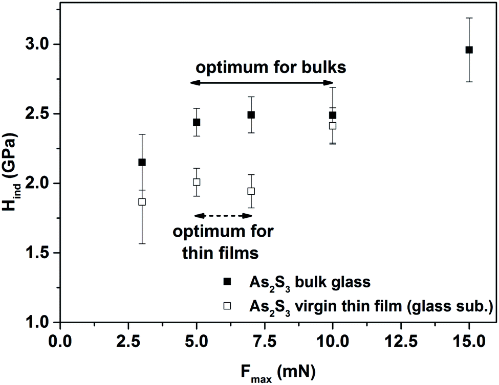 | ||
| Fig. 1 The dependency of nanohardness (Hind) on a different peak load (Fmax) for As2S3 bulk glass and virgin thin film evaporated onto a glass substrate. | ||
3. Results and discussion
3.1. Chemical composition and characteristics of the studied materials
The results of chemical composition analysis for all the prepared thin films in Table 1 are summarized. It is clear that for the bulk glasses the nominal chemical composition corresponds well with the results of the electron microprobe X-ray analysis. It also could be seen that the chemical composition of all prepared thin films was, with respect to the experimental error, comparable to that of the corresponding bulk glasses. Additionally, in the whole manuscript the samples are marked as As2S3 for As40S60 bulk glass and As39.0S61.0 thin film (both in atomic fractions); As2Se3 for As40Se60 bulk glass and As41.2S58.8 thin film (both in atomic fractions); and as As1Se99 for As1Se99 bulk glass and As0.5S99.5 thin film (both in atomic fractions). The glass transition temperatures, see Table 1, (determined as the mid-point by DSC) for the bulk glasses, correspond well to those reported in the literature.35,36 The effect of the so-called “useful impurity” for the As1Se99 bulk glass1,37 that causes an increase in the glass transition temperature even by the addition of 1 at% of As into pure amorphous Se (due to the cross-linking of the selenium matrix by arsenic atoms) is evident (for the Tg values38). Table 1 also shows the basic optical characteristics (the optical band gap (Eoptg) and refractive index (n)) for all prepared thin films evaporated onto a glass substrate. The optical band gap of As2S3 virgin thin film evaporated onto glass substrate is 2.38 eV while for As2Se3 and As1Se99 it decreases to 1.78 and 1.89 eV, respectively. The values of the optical band gap Eoptg correspond well to those reported in the literature.10,39| Sample | Bulk glasses | Thin films | |||||
|---|---|---|---|---|---|---|---|
| Chemical composition (at%) | Tg (°C) | Refractive index (−) | Chemical composition (at%) | Refractive index (−) | Eoptg (eV) | d (nm) | |
As![[thin space (1/6-em)]](https://www.rsc.org/images/entities/char_2009.gif) :X, where X = S, Se :X, where X = S, Se |
As:X, where X = S, Se |
||||||
| a The refractive index of As2S3 thin film evaporated onto glass substrate after the annealing. | |||||||
| As2S3 | 40:60 |
205 | 2.42 | 39.0:61.0 |
2.40, 2.41a | 2.38 | 3370 |
| As2Se3 | 40:60 |
190 | 2.84 | 41.2:58.8 |
2.69 | 1.78 | 3260 |
| As1Se99 | 1:99 |
55 | 2.52 | 0.5:99.5 |
2.49 | 1.89 | 3910 |
Finally, Table 1 also summarizes the values of all thin film thicknesses determined by the modified Swanepoel method.18 It should be noted that these are average values of the thin film thickness measured from 8 different places on the substrate. The typical conformity between the experimental and fit of experimental data is shown in Fig. 2A for the As2S3 thin film evaporated onto a glass substrate. It could be seen that the thickness of all thin films evaporated onto the glass substrate is in the range 3–4 μm. It also should be noted that the standard deviation in the determination of all thin film thicknesses by the modified Swanepoel method do not exceed 0.5%. The thickness of all thin films was also checked by SEM analysis on fresh samples broken perpendicularly to the direction of evaporation, and the comparable results, with respect to the 2% experimental error, were obtained as is shown for the As2S3 thin film evaporated onto the glass substrate in Fig. 2B.
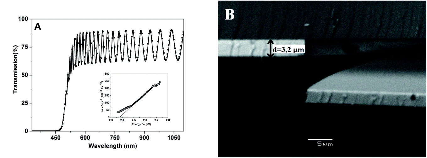 | ||
| Fig. 2 The experimental (solid line) and fit of calculated values (symbols) of spectral dependency of the optical transmission for the As2S3 virgin thin film evaporated onto a glass substrate (A), and SEM image of fresh As2S3 virgin thin film broken perpendicularly to the direction of evaporation (B). The inset in (A) shows the spectral dependency of the absorption coefficient for the As2S3 virgin thin film evaporated onto the glass substrate. | ||
3.2. Raman spectra of the bulk glasses and thin films
Fig. 3A gives the Raman spectra of As2S3 bulk glass and thin films evaporated onto glass and Si substrates, and as is well known, the spectra of the thin films are different to the spectra of bulk glass. The spectra of bulk glass consists of the main broad band with the maxima at ≈340 cm−1 corresponding to the presence of symmetric stretching vibration modes of AsS3/2 pyramidal units with two shoulders at ≈310 and 380 cm−1 attributed to the presence of the antisymmetric stretching vibration modes of AsS3/2 pyramidal units and As–S–As bridges, respectively. The weak bands near ≈190 and 230 cm−1 are attributed to the presence of the bending vibration mode of As–As molecular units. In contrast, the bands at ≈340 and 360 cm−1 dominate the spectra of As2S3 thin films evaporated onto glass and Si substrates, and they have been assigned to the symmetric and antisymmetric stretching vibration modes of As–S bond in β-As4S4 molecular units, respectively. The bands at ≈190 and 220 cm−1 in the bending vibration region have been attributed to the S–As–S bending mode in the As4S4 molecular units, and the band at ≈230 cm−1 has been associated with the bending of S2As–AsS2 structural units. The bands at ≈145 and 165 cm−1 correspond to the vibration in As4S4 molecular units, while the band at ≈134 cm−1 is connected to the presence of AsS3/2 pyramidal units.40–45 After the annealing, the Raman spectra of the As2S3 thin film evaporated onto glass substrate becomes comparable to that of bulk glass (Fig. 3A). Similar results are published in ref. 9, 46 and 47 and are explained by the temperature induced bond rearrangement and a network polymerization.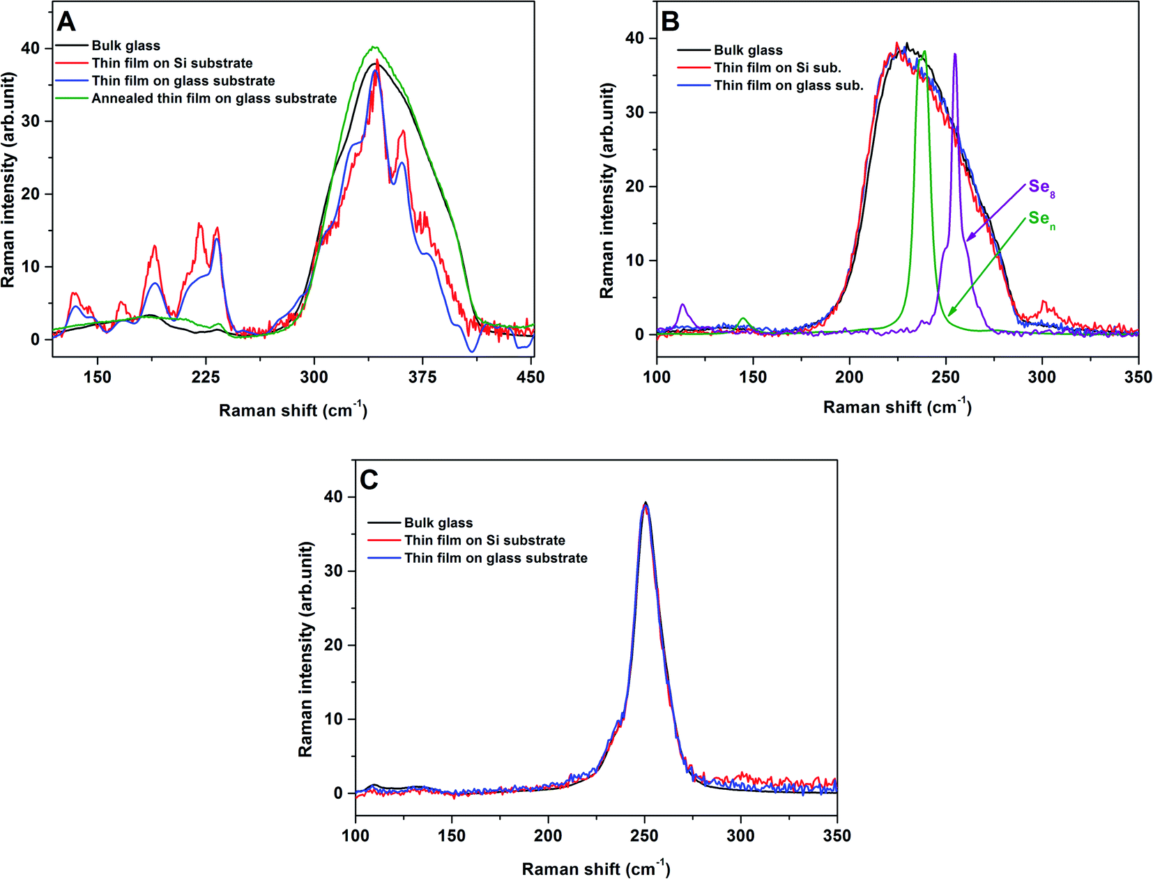 | ||
| Fig. 3 Raman spectra of As2S3 (A), As2Se3 (B) and As1Se99 (C) bulk glasses and thin films (virgin/annealed) evaporated onto glass and Si substrates. For comparison reasons, also included in (B) is the Raman spectra of pure glassy Se consisting mainly of Se8 rings or Sen chains according to ref. 62. | ||
Contrary to As2S3 bulk glass and thin films, the Raman spectra of As2Se3 bulk glass and thin films evaporated onto glass and Si substrates are practically identical (Fig. 3B). The Raman spectra of all the samples consist of a broad band between 200–300 cm−1 which is formed by overlapping the main band near 220–230 cm−1 connected with the stretching vibration modes of AsSe3/2 pyramidal units, the band near 235 cm−1 is attributed to the presence of –(Se–Se)n– (n ≥ 1) chain vibrations, and the band near 255 cm−1 is assigned to the presence of both Se8 rings and Se8 meandering chain vibrations.48 A comparable result for the Raman spectra of As1Se99 bulk glass and the corresponding thin films evaporated onto glass and Si substrates was also found, as shown Fig. 3C. In this case, the Raman spectra of all samples consist only of one main band over 250 cm−1 which is formed by the overlapping of the most intense band at 255 cm−1 and the band near 235 cm−1 and they were attributed as described above. Hence, the Raman spectra of all studied bulk glasses and thin films well corresponds to the literature data9,46–48 and practically no influence on the substrates was observed on the Raman spectra of the prepared thin films.
3.3. Density of the bulk glasses and thin films
Table 2 summarizes the Archimedean bulk glasses density (ρbulk) and the density of the corresponding thin films (ρfilm) evaporated onto different substrates. The bulk density varied from 3.1938 g cm−3 for As2S3 bulk glass to 4.557 and 4.2957 g cm−3 for As2Se3 and As1Se99 bulk glasses, respectively. Comparable trends for the density of bulk glasses and the density of corresponding thin films, were found. The density varied from 3.147 g cm−3 for the As2S3 thin film evaporated onto the glass substrate, to 4.227 and 4.198 g cm−3 for As2Se3 and As1Se99 thin films evaporated onto the same substrate, respectively. These values are comparable to those reported in the literature.36,49 The density for thin films evaporated onto Si substrate varied from 3.148 g cm−3 for As2S3 to 4.237 and 4.216 g cm−3 for As2Se3 and As1Se99, respectively. Thus almost negligible influence of substrate at the given films thickness (see Table 1) on the thin films density was observed (Table 2). The decrease of thin films density in comparison with the corresponding bulk glass equals ≈2 rel% for As2S3 and As1Se99, and to ≈8 rel% for As2Se3 materials (Table 2). Hence, it is seen that regardless of the chemical composition and also the used substrates for the preparation of thin films, the bulk glasses density (ρbulk) is higher than the density of the corresponding thin films (ρfilm). It also should be mentioned that the cumulative error (uncertainty) of the thin films density values, calculated according to ref. 50, do not exceed 0.5% in all cases (it varies from ≈0.016 to ≈0.021 g cm−3 based on the chemical composition and the substrate used for the evaporation). The comparable trend, as shown in this work, was also published by De Neufville et al.51 for the As2Se3 bulk glass and corresponding evaporated thin film. However, the authors also compared the density of As2S3 bulk glass and corresponding thin film and in this case, the density variation was opposite which was not commented by the authors. Table 2 additionally shows that the density of the As2S3 thin film increased to 3.160 g cm−3 after the annealing of this thin film.| Sample | ρbulka (g cm−3) | ρthin film on different substratesa (g cm−3) | ρbulk/Ø ρthin filmsa | |
|---|---|---|---|---|
| Glass | Si | |||
| a The number in the subscript expresses the highest value of uncertainty found in a similar manner to that one used previous in ref. 63.b The density (or ρbulk/Ø ρthin film ratio) for As2S3 thin film evaporated onto glass substrate after the annealing. | ||||
| As2S3 | 3.1938 | 3.147; 3.160b | 3.148 | 1.015/1.011b |
| As2Se3 | 4.5587 | 4.227 | 4.237 | 1.077 |
| As1Se99 | 4.2957 | 4.198 | 4.216 | 1.021 |
3.4. Refractive index
The refractive indices (n) for all the prepared bulk glasses and corresponding virgin thin films evaporated onto the glass substrates are shown in Table 1. The comparable values of the bulk glass refractive index, for example by Cardinal et al.,36 have been published. From Table 1 it is clear that: (i) regardless of the chemical composition, the refractive index of the thin films is lower than the refractive index of the corresponding bulk glasses, and (ii) the refractive index decrease is equal to ≈1 rel% for As2S3 and As1Se99 thin films, and ≈5 rel% for the As2Se3 thin film, in comparison with the corresponding bulk glasses. De Neufville et al.51 also show in their work that As2S3 bulk glass has a higher refractive index than the corresponding virgin thin film. The authors also found much higher difference in the refractive index than that reported in this work which, however, could be a consequence of different preparation conditions. Furthermore, the authors showed that the refractive index of virgin As2S3 thin film after annealing and illumination is almost the same as that of bulk glass. Additionally, Table 1 also shows that after annealing of the As2S3 virgin thin film evaporated onto glass substrate, the refractive index increased to the value of 2.41.We shall try to compare the changes in the refractive index and density of the bulk samples and virgin films employing the Lorentz–Lorenz relation (LLR): (n2 − 1)/(n2 + 2) = ρRm, Rm = 4πNAαm/3, where αm is the molecule polarizability and NA is the Avogadro number. Because we did not observe the dimension changes in the direction parallel to the substrate, we assume that the volume (V) changes of the film correspond mainly to the expansion, that is to an increase in the film thickness (d). In such a case: Δd/d = ΔV/V = −Δρ/ρ, (we assume: dx/x = Δx/x; where ΔX = Xann. − Xvir. or ΔX = Xbulk − Xvir.). Hence from LLR follows: Δn(LL) = [(Δρ/ρ) + (ΔRm/Rm)](n2 − 1)(n2 + 2)/6n, assuming that ΔRm/Rm ≠ 0. For the experimental values of refractive indices and densities of virgin films and bulk glasses, see Table 1, we obtain Δn(exp) = Δn(LLR) only assuming that ΔRm/Rm = −0.007, −0.036 and −0.012 for As2S3, As2Se3 and As1Se99, respectively. This means that in the considered cases the differences in the densities cannot be fully explained by the differences between refractive indices of the bulks and virgin thin films. However, with respect to the magnitude of ΔRm/Rm the values of Δρ/ρ play a major role in the observed Δn(exp) differences (Δρ/ρ = 0.0149, 0.0785 and 0.0233 for As2S3, As2Se3 and As1Se99, respectively). This finding is interesting with respect to the results of Raman spectroscopy as the structural differences between bulk and virgin thin film of As2Se3 and As1Se99 are very small in comparison with those of As2S3 (comparing Fig. 3A–C). We note that for As2Se3 quite small structural differences inferred from Raman spectroscopy between the bulk and virgin thin film in the work by Němec et al.10 and Treacy et al.52 were also found. For large structural differences for As2S3, see Fig. 3A, we observed the lowest change in Δρ/ρ. This we tentatively explain by assuming that a density decrease of As2S3 virgin thin film, associated with the depolymerization of the network and with an increase in disorder, is compensated by As4S4 structural units present in the virgin thin film having higher density (ρrealgar = 3.56 g cm−3/ρpararealgar = 3.52 g cm−3 (ref. 53)) than As2S3 bulk. Of interest is the fact that contrary to the As2S3 case, for both As1Se99 and As2Se3, there are only very subtle structural differences indicated by Raman spectroscopy, see Fig. 3B and C, while there are evident and higher differences in the density in comparison with the As2S3 case. We suppose that this finding could be qualitatively explained assuming that the major part of the observed density difference is attributed to higher empty volume in virgin As1Se99 and As2Se3 thin films. Hence the difference in the refractive index of As1Se99 and As2Se3 thin films and bulk, and the corresponding virgin thin films, is not associated with the large structural changes, but rather it can be attributed to a reduction of empty volume1 in the bulk samples, and of course to the changes in molar polarizability. Since ΔR = αm,bulk − αm,vir., the negative values of ΔR (see previous text) mean that αm,vir. > αm,bulk. Consequently one can speculate that higher disorder associated with the presence of wrong bonds, defect states, possible fluctuation in the bond length and bond distances can assist an increase of molar polarizability of As1Se99 and As2Se3 virgin thin films.
For similar comparison of the virgin and annealed states of the As2S3 thin film (the data in Tables 1 and 2), we can obtain Δn(LL) = 0.01 which is comparable to the experimental value, even for ΔRm/Rm = 0. This means, with respect to the experimental error, that Rm,vir. = Rm,ann. and hence αm,vir. = αm,ann.. This behavior needs further attention and will be the subject of further research.
3.5. The nanoindentation hardness of bulk glasses and thin films
Fig. 4 shows the representative force (F)–displacement (h) curve for the As2Se3 thin film evaporated onto a glass substrate, and the subtracted values of maximal displacement (hmax) at the set peak load (Fmax), and the slope of unloading curve (SBW = dF/dh). For all the bulk glasses and thin films evaporated onto different substrates, smooth F–h curves with residual depth upon complete unloading were observed. The homogeneous deformation of material indicates the absence of pop-ins (or displacement bursts) in the loading part, while no pop-out or elbow during unloading reveals clearly that no phase transformation occurs (see Fig. 4). Furthermore, the inset of Fig. 4 shows the residual imprint image, with the shape of the trigonal pyramid created by the pushing of a Berkovich type of tip into the material, on the specimen surface captured immediately post-indentation. Fig. 4 also illustrates that during the indentation no corner cracking occurs. Table 3 summarizes the values of hmax, Fmax and SBW subtracted from the individual force–displacement curves for the As2Se3 thin film evaporated onto the glass substrate. The values of contact depth (hc), using the Oliver–Pharr method (see eqn (3) in ref. 34), were calculated and based on the calibration, carried out on the fused silica reference sample, the values of Ac (the contact area) were determined. Finally, the Oliver–Pharr method was used (see eqn (5) in ref. 34) to extract the nanohardness (Hind) of the As2Se3 thin film as shown in Table 3. It could be seen that from the nine independent indentations the average nanohardness (Hind) of the As2Se3 thin film equals 1.88 GPa with standard deviation 0.05 GPa. The nanohardness (Hind) of the rest of the bulk glasses and the thin films on the different substrates was determined in the same way.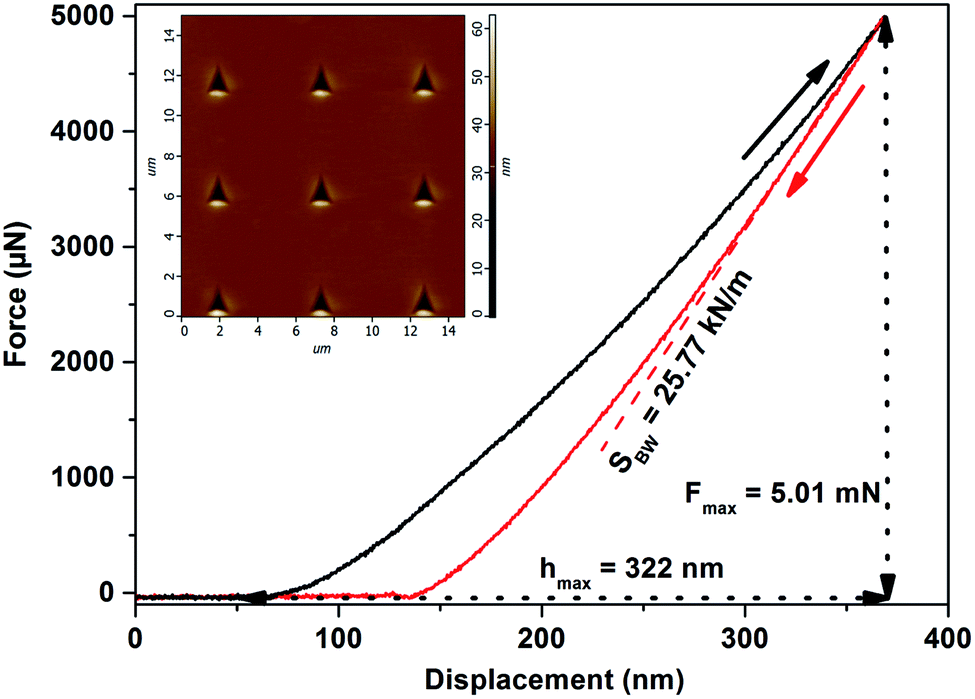 | ||
| Fig. 4 The representative force (F)–displacement (h) curve for the As2Se3 virgin thin film evaporated onto glass substrate, and the subtracted values of hmax, Fmax and SBW. The inset shows the residual imprint on the specimen surface. | ||
| N | hmax (nm) | Fmax (mN) | SBW (kN m−1) | hc (nm) | Ac (μm2) | Hind (GPa) |
|---|---|---|---|---|---|---|
| 1 | 322 | 4.96 | 26.45 | 181 | 2.70 | 1.8374 |
| 2 | 315 | 4.98 | 26.32 | 173 | 2.57 | 1.9353 |
| 3 | 325 | 4.97 | 24.87 | 175 | 2.60 | 1.9085 |
| 4 | 330 | 4.98 | 25.65 | 184 | 2.75 | 1.8137 |
| 5 | 326 | 4.98 | 25.15 | 177 | 2.64 | 1.8861 |
| 6 | 321 | 4.99 | 27.43 | 185 | 2.75 | 1.8156 |
| 7 | 320 | 4.98 | 25.69 | 175 | 2.60 | 1.9180 |
| 8 | 316 | 5.01 | 26.35 | 173 | 2.58 | 1.9434 |
| 9 | 322 | 5.01 | 25.77 | 176 | 2.62 | 1.9118 |
| Ar. mean | 1.88 | |||||
| SD | 0.05 |
It also should be mentioned that the peak load, Fmax, varied between 3–15 mN for all materials, while the optimum for the comparison of all bulk glasses and thin films evaporated onto different substrates was found at Fmax = 5 mN (see Fig. 1), and hence the nanohardness of all the samples was compared at this value. If a higher Fmax was used, the rule that the penetration depth of the tip was up to a maximum of 10% of the total thickness of the thin films, was not fulfilled, and the measured nanohardness could be influenced by the nanohardness of the substrate. On the other hand, for a lower Fmax, the experimental error was higher than 20%, probably due to surface defects, experimental noise etc.
Table 4 summarizes the nanohardness (Hind) of As2S3, As2Se3 and As1Se99 bulk glasses and the corresponding thin films evaporated onto different substrates. It could be seen that the almost comparable values of the Hind for As2S3 and As2Se3 bulk glasses were observed. The comparable trend was also published by Kavetskyy et al.54 However, the authors provided the values of microhardness for As2S3 and As2Se3 bulk glasses which were almost equal. The nanohardness, in our case, varied from 2.44 to 2.20 GPa for As2S3 and As2Se3 bulk glasses, respectively (Table 4). On the other hand, much lower nanohardness of As1Se99 (Hind = 1.29 GPa) in comparison with the As2S3 and As2Se3 bulk glasses was observed. This could be connected with its structure and it differs significantly in comparison with other prepared materials, see Fig. 3. In the case of As1Se99, mainly –(Se–Se)n– (n ≥ 1) chains and both Se8 rings and Se8 meandering chains were found.48 The decrease of As1Se99 bulk glass nanohardness in comparison with As2Se3 bulk glass is in harmony with the results published by Guin et al.21 The authors showed that Vicker’s or Meyer’s hardness increases with increasing average coordination number of Ge–Se chalcogenide bulk glasses and they supposed that the main reason for such behavior is the topological nature. Table 4 also compares the nanohardness of all the bulk glasses under the different peak load (Fmax), while the trend in Hind was not changed. This trend in nanohardness is in harmony with the data of microhardness published in the literature55 for the same bulk glasses. We realize that this comparison of our results with that in the literature is not entirely correct, but to our best knowledge, there are no relevant data for nanohardness, for the glasses studied by us, for true comparison.
| Sample | Bulk glasses | Thin films nanohardness (GPa), (Fmax = 5 mN) | |||
|---|---|---|---|---|---|
| Nanohardness (GPa) | Microhardness (kg mm−2) | ||||
| Fmax = 5 mN | Fmax = 10 mN | Data taken from ref. 55 | Glass substrate | Si substrate | |
| a The nanohardness of As2S3 thin film evaporated onto a glass substrate after annealing. | |||||
| As2S3 | 2.44 | 2.49 | 1.33 | 2.01, 2.08a | 1.99 |
| As2Se3 | 2.20 | 2.41 | 1.24 | 1.88 | 1.87 |
| As1Se99 | 1.29 | 1.63 | 0.43 | 1.08 | — |
With some caution in comparing nanohardness and microhardness values, we show in Fig. 5, the empirical correlation Hind and Hv values versus Tg values, where Hv and Tg values for Ch–As2Ch3 (Ch = S, Se) glasses were taken from ref. 55. It is evident that this correlation satisfies the relation Tg = K(H − B) suggested by Shkol’nikov.56 Because for Se–As2Se3 glasses the relation between Tg and the average coordination number (<r>) is linear, see e.g. the work of Boolchand et al.,57 it is not surprising that the relation between Hv values for Se–As2Se3 glasses and Tg, <r>, inclusive of our Hind values, should also be linear as found by Hach et al.58
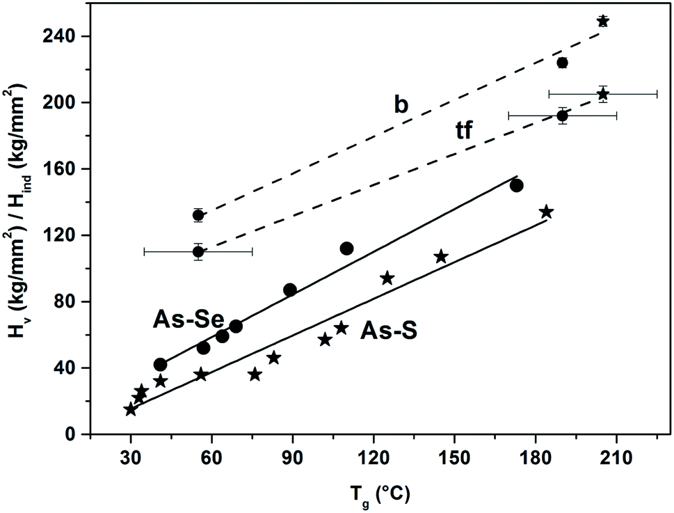 | ||
| Fig. 5 The dependency of microhardness (Hv) on a glass transition temperature (Tg) for As–S (solid line with stars, AsxS(100−x), 9.1 ≤ x ≤ 40) and As–Se (solid line with circles, AsxSe(100−x), 0 ≤ x ≤ 40) bulk glasses according to ref. 55. Our data on nanohardness (Hind) were added to the graph after unit conversion for both As–S and As–Se bulk glasses (dashed line marked as “b” with star and circles, respectively) and As–S and As–Se thin films (dashed line marked as “tf”, with star and circles, respectively). It also should be noted that we assumed Tg(film) ± 20 °C = Tg(bulk). In all cases, the lines are included as mere guides for the eye. | ||
Table 4 also shows the nanohardness (Hind) of all prepared thin films evaporated onto the glass substrate and it could be seen that their nanohardness is lower in all cases than that of the corresponding bulk glasses. The nanohardness varied from 2.01 to 1.88 GPa for As2S3 and As2Se3 thin films evaporated onto the glass substrate, respectively. Furthermore, the same trend as for the bulk glasses was found, thus the nanohardness of As1Se99 thin film evaporated onto the glass substrate (Hind = 1.08 GPa) was much lower in comparison with As2S3 and As2Se3 thin films evaporated onto the same substrate (Table 4). The nanohardness (Hind) of the thin films was lower in comparison with bulk glasses in the range between 0.21–0.43 GPa depending on the chemical composition. The decrease of the thin films nanohardness in comparison with the corresponding bulk glass equals ≈21 rel% and 19 rel% for As2S3 and As1Se99 glasses, and ≈17 rel% for As2Se3 glass. The comparable trend was also published by Shchurova et al.59 and they showed in their work that the mechanical properties like Young’s modulus or microhardness of As2S3 and As2Se3 bulk glasses among others are higher in comparison with the corresponding thin films. The authors attributed these to the packing density, that is the ratio between the films and bulk glasses density. Table 4 also shows that the influence of different substrates (glass and Si) used for the preparation of thin films was, with respect to the experimental, almost negligible and this is in harmony with the data published by Pelegri et al.60 and Menčík et al.61 These authors, however, did not study chalcogenide glasses.
The decrease in the thin film nanohardness in comparison with the corresponding bulk glasses is in harmony with our previously mentioned results in chapters 3.3 and 3.4, thus with a decrease of density and refractive index of the thin films with respect to their corresponding bulk glasses. The results for As2S3 and As1Se99 materials are comparable, thus the decrease of refractive index and density of thin films in comparison with their corresponding bulk glasses was in the order of 1–2 rel%, while the decrease of nanohardness of thin films in comparison with their corresponding bulk glasses was ≈20 rel% (see Tables 1, 2 and 4).
Additionally, the difference not only between the refractive index and density of As2S3 bulk glass and corresponding thin film, but also between their structures, was observed. The structure depolymerization for the As2S3 virgin thin film was observed, which leads to the decrease in the thin film cohesion, and this in all probability also contributed to the highest decrease of nanohardness in comparison with the corresponding bulk glass. After the annealing of the As2S3 thin film which was accompanied with the structure polymerization, the structure became comparable to that of bulk glass and the nanohardness of As2S3 thin film increased to 2.08 GPa as shown in Table 4. This increase in the As2S3 thin film nanohardness, however, did not have much influence on the relative difference between the nanohardness of the As2S3 thin film and its corresponding bulk glass. Furthermore, although the highest relative difference between the As2Se3 thin film and corresponding bulk glass was found from the point of refractive index and density (see Table 1 and 2), that the nanohardness difference between the As2Se3 thin film and corresponding bulk glass was lower (17 rel%) in comparison with the As2S3 and As1Se99 materials (≈20 rel%). However, this does not change the fact that the nanohardness of all thin films was lower than the corresponding bulk glasses, and the reason for such a difference in behavior of the As2Se3 materials in comparison with As2S3 and As1Se99 samples will be the subject of further research.
4. Conclusion
Our results can be summarized as follows:(i) Density, structure and nanohardness were compared for all the bulk glasses and corresponding thin films, whose density, using their accurate weighing, was determined.
(ii) A major part of the observed changes in the refractive index between virgin films and the corresponding bulk glasses was explained, using the Lorentz–Lorenz relation, mainly by lowering the thin films density in comparison with the density of the corresponding bulk glasses.
(iii) The Raman spectra showed a similar structural arrangement for both the As2Se3 and As1Se99 bulk glasses and thin films and, as is well known, confirmed the different structural arrangement for the As2S3 bulk and virgin thin films. At the same time, the differences in the density between As2Se3 and As1Se99 bulk glasses and their corresponding thin films is much higher than the differences in the density of As2S3 and the corresponding thin films. This is explained by the role of empty volume in the case of the bulk glasses and As2Se3 and As1Se99 thin films, and by depolymerization in the As2S3 thin film.
(iv) Last, but not the least, the nanohardness of all bulk glasses and corresponding thin films was also compared. The nanohardness of all thin films was in all cases lower than that of the corresponding bulk glasses. This result is in harmony with lower values of thin films density with the respect to their corresponding bulk glasses. Linear correlation between the nanohardness and the glass transition temperature was found.
Conflicts of interest
There are no conflicts to declare.Acknowledgements
Support from the Faculty of Chemical Technology, University of Pardubice (FChT UPa) is highly acknowledged by all authors. The financial support from the Grant Agency of the Czech Republic (GA CR), project No. 19-11814S is greatly appreciated. We are also indebted to Prof. Václav Švorčík from the Department of Solid State Engineering, University of Chemical Technology, Prague for the very precise UMX balance usage, and to Prof. Andréa Kalendová from the Institute of Chemistry and Technology of Macromolecular Materials, University of Pardubice for the SOLVER NEXT, AFM usage.References
- R. Zallen, The Physics in Amorphous Solids, Wiley-VCH Verlag GmbH & Co. KGaA, 2007 Search PubMed.
- J.-L. Adam and X. E. Zhang, Chalcogenide Glasses Preparation, Properties and Applications, Woodhead Publishing Ltd, 2013 Search PubMed.
- R. I. Alekberov, S. I. Mekhtiyeva, A. I. Isayev and M. Fabian, J. Non-Cryst. Solids, 2017, 470, 152–159 CrossRef CAS.
- R. I. Alekberov, S. I. Mekhtiyeva, A. I. Isayev, M. Fabian, Q. Tian and L. Almasy, Chalcogenide Lett., 2017, 14, 79–85 CAS.
- R. I. Alekberov, A. I. Isayev, S. I. Mekhtiyeva and M. Fabian, Phys. B, 2018, 550, 367–375 CrossRef CAS.
- H. A. Lorentz, Ann. Phys., 1880, 9, 641–665 CrossRef.
- L. Lorenz, Ann. Phys., 1880, 11, 70–103 CrossRef.
- Y. Saito, S. Hatayama, Y. Shuang, S. Shindo, P. Fons, A. V. Kolobov, K. Kobayashi and Y. Sutou, Appl. Phys. Express, 2019, 12, 051008 CrossRef CAS.
- M. Frumar, Z. Polak, M. Vlcek and Z. Cernosek, J. Non-Cryst. Solids, 1997, 221, 27–33 CrossRef CAS.
- P. Němec, J. Jedelsky, M. Frumar, M. Stabl and M. Vlcek, J. Phys. Chem. Solids, 2004, 65, 1253–1258 CrossRef.
- M. Samuelsson, D. Lundin, J. Jensen, M. A. Raadu, J. T. Gudmundsson and U. Helmersson, Surf. Coat. Technol., 2010, 205, 591–596 CrossRef CAS.
- A. Waseda, K. Fujii and N. Taketoshi, IEEE Trans. Instrum. Meas., 2005, 54, 882–885 CrossRef.
- P. Viščor and D. Allan, Thin Solid Films, 1979, 62, 259–263 CrossRef.
- M. Yasaka, Rigaku J., 2010, 26, 1–9 CAS.
- B. Ilic, S. Krylov and H. Craighead, Proc. IEEE, 2009, 650–653 Search PubMed.
- W. E. Wallace, D. L. Jacobson, M. Arif and A. Ioffe, Appl. Phys. Lett., 1999, 74, 469–471 CrossRef CAS.
- H. F. Xiang, Z. X. Xu, V. A. L. Roy, C. M. Che and P. T. Lai, Rev. Sci. Instrum., 2007, 78, 034104 CrossRef.
- R. Swanepoel, J. Phys. E: Sci. Instrum., 1983, 16, 1214–1222 CrossRef CAS.
- J. B. Pethica, R. Hutchings and W. C. Oliver, Philos. Mag. A, 1983, 48, 593–606 CrossRef CAS.
- F. Spaepen and A. L. Shull, Curr. Opin. Solid State Mater. Sci., 1996, 1, 679–683 CrossRef CAS.
- J. P. Guin, T. Rouxel, J. C. Sangleboeuf, I. Melscoet and J. Lucas, J. Am. Ceram. Soc., 2002, 85, 1545–1552 CrossRef CAS.
- M. L. Trunov, S. N. Dub, P. M. Nagy and S. Kokenyesi, J. Phys. Chem. Solids, 2007, 68, 1062–1068 CrossRef CAS.
- T. Sabapathy, M. Kiran, A. Ayiriveetil, A. K. Kar, U. Ramamurty and S. Asokan, Opt. Mater. Express, 2013, 3, 684–690 CrossRef CAS.
- J. N. Ding, G. X. Xie, Z. Fan, Y. Z. Fu and Z. Y. Ling, J. Wuhan Univ. Technol., 2007, 22, 196–200 CrossRef CAS.
- T. M. Rajakumar, V. Uma and R. Chandramani, Indian J. Pure Appl. Phys., 2013, 51, 131–137 CAS.
- A. G. Prabhudessai, S. Balaji, K. Biswas, R. Dasgupta, P. Sarkar and K. Annapurna, J. Non-Cryst. Solids, 2019, 507, 56–65 CrossRef CAS.
- P. Kutalek, E. Cernoskova, L. Benes, P. Knotek, Z. Cernosek and L. Tichy, J. Non-Cryst. Solids, 2017, 478, 75–78 CrossRef CAS.
- J. Tauc, Amorphous and liquid semiconductors, ed. J. Tauc, Plenum, New York, 1974 Search PubMed.
- R. Shuker and R. W. Gammon, Phys. Rev. Lett., 1970, 25, 222–225 CrossRef CAS.
- E. Márquez, J. M. GonzalezLeal, R. Jimenez Garay, S. R. Lukic and D. M. Petrovic, J. Phys. D: Appl. Phys., 1997, 30, 690–702 CrossRef.
- J. M. S. Prewitt and M. L. Mendelsohn, Ann. N. Y. Acad. Sci., 1966, 128, 1035–1053 CrossRef CAS.
- P. K. Sahoo, S. Soltani and A. K. C. Wong, Computer Vision, Graphics, and Image Processing, 1988, vol. 41, pp. 233–260 Search PubMed.
- P. Knotek, M. Vlcek, M. Kincl and L. Tichy, Thin Solid Films, 2012, 520, 5472–5478 CrossRef CAS.
- W. C. Oliver and G. M. Pharr, J. Mater. Res., 2004, 19, 3–20 CrossRef CAS.
- S. Tsuchihashi and Y. Kawamoto, J. Non-Cryst. Solids, 1971, 5, 286–305 CrossRef CAS.
- T. Cardinal, K. A. Richardson, H. Shim, A. Schulte, R. Beatty, K. Le Foulgoc, C. Meneghini, J. F. Viens and A. Villeneuve, J. Non-Cryst. Solids, 1999, 256, 353–360 CrossRef.
- V. I. Mikla and V. V. Mikla, J. Optoelectron. Adv. Mater., 2010, 12, 1827–1839 CAS.
- J. Holubova, Z. Cernosek and E. Cernoskova, J. Non-Cryst. Solids, 2009, 355, 2050–2053 CrossRef CAS.
- R. Todorov, D. Tsankov, J. Pirov and K. Petkov, J. Phys. D: Appl. Phys., 2011, 44, 305401 CrossRef.
- R. P. Wang, S. J. Madden, C. J. Zha, A. V. Rode and B. Luther-Davies, J. Appl. Phys., 2006, 100, 063524 CrossRef.
- R. Golovchak, O. Shpotyuk, J. S. Mccloy, B. J. Riley, C. F. Windisch, S. K. Sundaram, A. Kovalskiy and H. Jain, Philos. Mag., 2010, 90, 4489–4501 CrossRef CAS.
- D. Y. Choi, S. Madden, A. Rode, R. P. Wang and B. Luther-Davies, J. Appl. Phys., 2007, 102, 083532 CrossRef.
- V. I. Mikla and V. V. Mikla, Optoelectron. Adv. Mater., Rapid Commun., 2007, 1, 272–276 CAS.
- P. Nemec, J. Jedelsky, M. Frumar, Z. Cernosek and M. Vlcek, J. Non-Cryst. Solids, 2005, 351, 3497–3502 CrossRef CAS.
- M. L. Slade and R. Zallen, Solid State Commun., 1979, 30, 357–360 CrossRef CAS.
- D. Y. Choi, A. Wade, S. Madden, R. P. Wang, D. Bulla and B. Luther-Davies, Phys. Procedia, 2013, 48, 196–205 CrossRef CAS.
- Z. Polak, M. Frumar and B. Frumarova, Thin Solid Films, 1999, 343, 484–487 CrossRef.
- G. Lucovsky, Physics of Selenium and Tellurium, Springer-Verlag Berlin, 1979 Search PubMed.
- Y. Ito, S. Kashida and K. Murase, Solid State Commun., 1988, 65, 449–452 CrossRef CAS.
- Harvard University, Department of Physics, 2007, http://ipl.physics.harvard.edu/wp-uploads/2013/03/PS3E.
- J. P. De Neufville, S. C. Moss and S. R. Ovshinsky, J. Non-Cryst. Solids, 1974, 13, 191–223 CrossRef CAS.
- D. J. Treacy, P. C. Taylor and P. B. Klein, Solid State Commun., 1979, 32, 423–427 CrossRef CAS.
- P. Bonazzi, S. Menchetti and G. Pratesi, Am. Mineral., 1995, 80, 400–403 CAS.
- T. Kavetskyy, J. Borc, K. Sangwal and V. Tsmots, J. Optoelectron. Adv. Mater., 2010, 12, 2082–2091 CAS.
- Z. U. Borisova, Glassy Semiconductors, Plenum Press, New York, 1981 Search PubMed.
- E. V. Shkol’nikov, Sov. J. Glass Phys. Chem., 1985, 11(1), 50–55 Search PubMed.
- P. Boolchand, D. G. Georgiev, T. Qu, F. Wang, L. Cai and S. Chakravarty, C. R. Chim., 2002, 5, 713–724 CrossRef CAS.
- C. T. Hach, K. CerquaRichardson, J. R. Varner and W. C. LaCourse, J. Non-Cryst. Solids, 1997, 209, 159–165 CrossRef CAS.
- T. N. Shchurova and N. D. Savchenko, J. Optoelectron. Adv. Mater., 2001, 3, 491–498 CAS.
- A. A. Pelegri and X. Huang, Compos. Sci. Technol., 2008, 68, 147–155 CrossRef CAS.
- J. Menčík, in Emerging Nanotechnologies in Dentistry (Second Edition), Micro and Nano Technologies, William Andrew Applied Science Publishers, 2018 Search PubMed.
- J. Holubova, Z. Cernosek and E. Cernoskova, J. Optoelectron. Adv. Mater., 2007, 9, 1979–1984 CAS.
- L. Tichý, H. Tichá, P. Nagels, R. Callaerts, R. Mertens and M. Vlcek, Mater. Lett., 1999, 39, 122–128 CrossRef.
Footnote |
| † Electronic supplementary information (ESI) available. See DOI: 10.1039/d0ra08939g |
| This journal is © The Royal Society of Chemistry 2020 |