
 Open Access Article
 This Open Access Article is licensed under a Creative Commons Attribution-Non Commercial 3.0 Unported Licence
Insights into ultrafast charge-pair dynamics in P3HT:PCBM devices under the influence of static electric fields†
Debkumar Rana ,
Vladislav Jovanov,
Veit Wagner,
Arnulf Materny* and
Patrice Donfack*
,
Vladislav Jovanov,
Veit Wagner,
Arnulf Materny* and
Patrice Donfack*
Physics and Earth Sciences, Jacobs University Bremen, Campus Ring 1, 28759 Bremen, Germany. E-mail: p.donfack@jacobs-university.de; a.materny@jacobs-university.de
First published on 25th November 2020
Abstract
Polymer-fullerene blends based on poly(3-hexylthiophene-2,5-diyl) (P3HT) and phenyl-C61-butyric-acid methyl ester (PCBM) have been extensively studied as promising bulk heterojunction materials for organic semiconductor devices with improved performance. In these donor–acceptor systems where the bulk morphology plays a crucial role, the generation and subsequent decay mechanisms of photoexcitation species are still not completely understood. In this work, we use femtosecond transient absorption spectroscopy to investigate P3HT:PCBM diodes under the influence of applied static electric fields in comparison to P3HT:PCBM thin films. At the same time, we try to present a detailed overview about work already done on these donor–acceptor systems. The excited state dynamics obtained at 638 nm from P3HT:PCBM thin films are found to be similar to those observed earlier in neat P3HT films, while those obtained in the P3HT:PCBM devices are affected by field-induced exciton dissociation, resulting not only in comparatively slower decay dynamics, but also in bimolecular deactivation processes. External electric fields are expected to enhance charge generation in the investigated P3HT:PCBM devices by dissociating excitons and loosely bound intermediate species like polaron pairs (PPs) and charge transfer (CT) excitons, which can already dissociate only due to the intrinsic fields at the donor–acceptor interfaces. Our results clearly establish the formation of PP-like transient species different from CT excitons in the P3HT:PCBM devices as a result of a field-induced diffusion-controlled exciton dissociation process. We find that the loosely bound transient species formed in this way also are reduced in part via a bimolecular annihilation process resulting in charge loss in typical donor–acceptor P3HT:PCBM bulk heterojunction semiconductor devices, which is a rather interesting finding important for a better understanding of the performance of these devices.
1 Introduction
The light-to-current conversion process is the basis of solar cell devices. In the last few decades, many active materials have been used to produce efficient photovoltaic systems. While in most applications, solar cells are built from inorganic semiconductor materials, the exciting properties of organic molecules have initiated growing research interest in organic photovoltaic devices. In order to optimize their efficiency, a detailed understanding of the processes occurring during the light-to-current conversion is important. The efficiency of the light-induced generation of free charge carriers still has to be increased and therefore also possible loss-channels have to be identified. This is not trivial since there are different charge loss channels, which can be influenced by various parameters like donor–acceptor interface properties or also electric fields. It is well known that many conjugated polymers have semiconductor-like properties. These properties are determined by the π–π* interaction of the pz orbitals, which are delocalized along the polymer backbone. This π and π* orbitals form the highest occupied molecular orbital (HOMO) and lowest unoccupied molecular orbital (LUMO) in the conjugated polymeric systems, respectively. Compared to the inorganic semiconductor systems, HOMO and LUMO take the role of the valence and conduction band, respectively. In these materials, the band gap is typically high and the dielectric constant is relatively small. The primary photogenerated species in conjugated polymer systems is an electron–hole pair, which due to the small dielectric constant of the organic material is a Frenkel-type exciton. This type of exciton is strongly bound (0.3–1 eV) and localized on one molecular unit. As will be explained in the following, the generation of the exciton is followed by the formation of other kinds of charge pairs as well as isolated charges via a direct or an indirect process. The charge generation is the step, which finally is required in order to generate the desired electric energy.Organic solar cells made by blending a conjugated polymer as a donor material with an electron acceptor material have been in the spotlight of semiconductor research since a few decades due to their potential for novel applications.1 Power conversion efficiencies for such organic solar cells from 10 to 14% have been reported.2–7 Nevertheless, the mechanism of charge-carrier generation in organic solar cells is still a matter of debate. Continuous effort for device optimization has been put mainly into designing the polymers or modifying the device-layer structures while fundamental processes behind photocurrent generation are still not fully understood. There is considerable experimental evidence of charge formation from the initially generated excitons.8–10 It is also well known that the exciton separation process into charges happens through intermediate steps consisting of loosely Coulomb-bound states.11–15 To describe such intermediate states, a varying nomenclature has been introduced, including polaron pair (PP), electron–hole pair, charge pair, and the more familiar so-called charge transfer (CT) exciton. The precise mechanisms, by which these bound states split, are still under debate, since their understanding also depends on the nature of the interfacial regions. In brief, the PP features a charge transfer exciton but with the subtle difference that a dedicated lattice distortion is associated with each charge in the pair.
Charge generation in organic semiconductor blends is primarily initiated by light absorption in the polymer or the fullerene domain, eventually forming excitons exhibiting a finite diffusion length of about 3–10 nm.16,17 The exciton-diffusion length imposes a severe limitation on the maximum length scale of polymer-fullerene phase separation in the blend. In general, polymer light absorption is responsible for most of the photocurrent generation. The intermixed donor–acceptor domains in the blend play a key role for both the exciton dissociation and the photocurrent generation.18,19 Exciton dissociation happens mostly at the interface between the donor and acceptor materials and a large interfacial area is needed for an efficient dissociation process. In practice, increased exciton dissociation efficiency is usually achieved by using a so-called bulk heterojunction mixture of the donor and acceptor materials. The heterojunction mixture tremendously increases the donor/acceptor interfacial area because many interfaces are distributed within the mixture of the two semiconductor types and the nature of the intermixed interfacial phase is crucial. It is well documented that, for optimal morphologies, the domain size of the donor or acceptor material should be about twice the diffusion length of the photogenerated excitons.20 To fulfill this, a bi-continuous organization of different phases is needed. Ultimately, during film deposition, the intermixed phase organization depends on several factors including among others the solvent used, annealing steps, and the ratio between donor and acceptor material.21 Recent ultrafast transient photoabsorption (PA) studies have provided evidence that efficient charge generation and dissociation are associated with the tendency of PCBM to form pure aggregated domains22,23 in polymer-fullerene blends with a PCBM content above the miscibility threshold (i.e., the solubility threshold of a solute in another liquid).24 The resulting phase-separated PCBM domains help to provide highly delocalized acceptor states, which allow efficient electron–hole dissociation.25
Organic solar cells based on blending poly(3-hexylthiophene-2,5-diyl) (P3HT) and phenyl-C61-butyric-acid methyl ester (PCBM) have been studied extensively. Charge generation and recombination dynamics in this P3HT:PCBM system were also reported earlier.26–28 In this connection, several studies have shown that the ultrafast electron transfer from P3HT to PCBM occurs on a time scale of less than 100 fs![[thin space (1/6-em)]](https://www.rsc.org/images/entities/char_2009.gif) 28,29 while the hole transfer from PCBM to P3HT happens within less than 250 fs.28 These processes involve excitons and more specifically CT excitons diffusing near the donor–acceptor interface. Several photogenerated species corresponding to different PA bands can be observed following photoexcitation in neat P3HT as well as in P3HT:PCBM.18,30,31 In brief, hot excitons generated via the initial photoexcitation process can relax on an ultrafast time scale (<100 fs) to produce different species causing three main and broad PA bands around 1100, 650 and 900 nm,29–31 which have been assigned to singlet exciton, polaron-pair, and polaron, respectively. Previous studies have shown that the amount of polarons is initially less and then increases with the excitation fluence. Singlet excitons can further dissociate into polarons after migrating to favorable energy sites such as the donor/acceptor interfaces. The assignment of the PA band around 650 nm is complex because of various overlapping contributions which had previously been tentatively attributed to different photogenerated species including hole polarons,29 delocalized polarons,30 and PPs,32 and to electro-absorption.29 Therefore, transient absorption spectroscopy around 650 nm is normally not sufficient to describe the different contributing species. For instance, while the 650 nm PA observed in P3HT-only films in earlier studies was very often attributed to photoinduced polaron-pair absorption, the same PA band observed in P3HT:PCBM in a recent study31 was assigned to delocalized polarons. On the other hand, in a study using sub-micrometer resolution microscopy, Grancini et al.33 generally referred to the species responsible for a PA observed around 650 nm in thin films of P3HT and P3HT:PCBM blend as a charge transfer state (CTS), but these authors also drew the attention to the fact that this state had already been described using different terms such as bound polaron pair, bound electron–hole pair, geminate pair, and CTS. Moreover, despite the lack of a more specific assignment of the broad 650 nm PA band in the P3HT:PCBM donor–acceptor system studied in other works, it is nevertheless important to note that the different species contributing to this PA band differ in their decay kinetics.34
28,29 while the hole transfer from PCBM to P3HT happens within less than 250 fs.28 These processes involve excitons and more specifically CT excitons diffusing near the donor–acceptor interface. Several photogenerated species corresponding to different PA bands can be observed following photoexcitation in neat P3HT as well as in P3HT:PCBM.18,30,31 In brief, hot excitons generated via the initial photoexcitation process can relax on an ultrafast time scale (<100 fs) to produce different species causing three main and broad PA bands around 1100, 650 and 900 nm,29–31 which have been assigned to singlet exciton, polaron-pair, and polaron, respectively. Previous studies have shown that the amount of polarons is initially less and then increases with the excitation fluence. Singlet excitons can further dissociate into polarons after migrating to favorable energy sites such as the donor/acceptor interfaces. The assignment of the PA band around 650 nm is complex because of various overlapping contributions which had previously been tentatively attributed to different photogenerated species including hole polarons,29 delocalized polarons,30 and PPs,32 and to electro-absorption.29 Therefore, transient absorption spectroscopy around 650 nm is normally not sufficient to describe the different contributing species. For instance, while the 650 nm PA observed in P3HT-only films in earlier studies was very often attributed to photoinduced polaron-pair absorption, the same PA band observed in P3HT:PCBM in a recent study31 was assigned to delocalized polarons. On the other hand, in a study using sub-micrometer resolution microscopy, Grancini et al.33 generally referred to the species responsible for a PA observed around 650 nm in thin films of P3HT and P3HT:PCBM blend as a charge transfer state (CTS), but these authors also drew the attention to the fact that this state had already been described using different terms such as bound polaron pair, bound electron–hole pair, geminate pair, and CTS. Moreover, despite the lack of a more specific assignment of the broad 650 nm PA band in the P3HT:PCBM donor–acceptor system studied in other works, it is nevertheless important to note that the different species contributing to this PA band differ in their decay kinetics.34
Therefore, summarizing the above discussions on the PA band assignment, a major contribution from PPs to the 650 nm PA dynamics in P3HT and P3HT:PCBM films seems to be sensible. Regarding other PA bands assigned to singlet excitons and separated polarons, an investigation of their dynamics as function of an electric field would be of interest and could be compared to earlier studies performed without applying external fields. The present work focuses on the dynamics probed around 650 nm (we have chosen a probe wavelength of 638 nm within this PA band), which proved to be relevant in many earlier studies due to the important role PPs play in the overall light-to-charge conversion process.31,35–37 Detailed information about the formation and decay processes of PPs in neat P3HT was derived earlier from the 650 nm PA dynamics studies31,35,37–39 including our recent study,35 which enables us to directly compare our results obtained from P3HT thin films and P3HT-only diodes with the new data resulting from the measurements on P3HT:PCBM thin films and devices.
On the basis of the earlier studies, it is clear that following the optical absorption (exciton formation), exciton dissociation into charges across the donor–acceptor interfaces can occur spontaneously with the help of the intrinsic interfacial field without an additional external electric field.40–43 Nevertheless, although, an external electric field is not required for the spontaneous generation of charges in donor–acceptor systems, the overall charge generation will be affected by the presence of an electric field in a working device. It has been previously reported by others that the external electric field suppresses bimolecular recombination processes during charge extraction.44–46 With the present work, we aim to shed more light on the consequences of the possible formation of intermediate states during charge separation when a static electric field is also present. While we mainly monitor dissociation processes of transient electron–hole pairs, we also look for indications of the influence of bimolecular annihilation processes, which together with recombination processes would be charge-loss mechanisms limiting organic solar cell efficiency. In our previous study, we have investigated the formation of PPs during charge separation in a P3HT-only diode (P3HT film sandwiched between two charge transport layers with different work functions and with electrode contacts made from different materials) under the influence of static electric fields,35 and we find some parallel behavior when probing the dynamics of the PA band around 650 nm in P3HT:PCBM as will be shown in the following.
While the external electric field effects on exciton and charge dynamics have been already reported,47,48 establishing a comprehensive and detailed picture of the field effect on possible intermediate states lying between the tightly bound exciton and the fully separated charges is a difficult task. Varying the relative donor/acceptor composition, we have investigated both the applied electric field effects and the influence of phase morphology on the PA dynamics probed at 638 nm in P3HT:PCBM systems. For this, we have additionally employed transient absorption anisotropy measurements to see morphology-relevant effects on the measured dynamics.
2 Experimental details
2.1 Femtosecond transient absorption spectroscopy
The details of the experimental setup used for time-resolved PA measurements can be found elsewhere.35 Briefly, the output of a regenerative amplifier Ti:sapphire laser system (CPA 2010, Clark-MXR) producing laser pulses with 775 nm central wavelength, 1 mJ energy per pulse, 150 fs pulse width, and 1 kHz repetition rate was used to pump two optical parametric amplifiers (TOPAS, Light Conversion) in order to generate the pump and probe pulses with center wavelengths of 520 nm and 638 nm, respectively. Both pump and probe beams were compressed to less than 120 fs pulse width using a set of prism compressors and then made collinear and kept with parallel polarizations for the measurements.2.2 Thin film deposition and device fabrication
P3HT:PCBM blend thin films were fabricated under ambient conditions. First, glass substrates were cleaned with acetone and 2-propanol, then exposed to UV light in a UV-ozone cleaner for 10 min in order to remove any residual solvent and used to deposit P3HT:PCBM films by doctor blading. The solution concentration was varied to obtain 1:1 and 2:1 P3HT:PCBM weight ratios. The measured thickness of the deposited films was 200 nm. Two devices in the solar cell configuration with a diode-like behavior due to asymmetric contacts were fabricated as described earlier35 using the P3HT:PCBM thin films with different weight ratios as active layers (see Fig. 1). The thin films and the devices were optically and electrically characterized; their UV-VIS absorption spectra and current–voltage (IV) characteristics are shown in Fig. S1 and S2 of the ESI,† respectively.
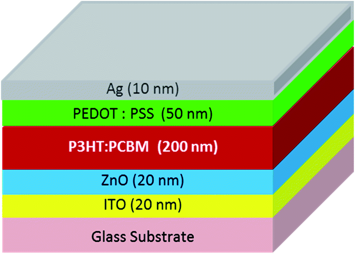 | ||
| Fig. 1 Schematic solar cell layer stack configuration of P3HT:PCBM diode. | ||
3 Results and discussion
First insights into static electric field effects on PP dynamics were discussed in an earlier study using a P3HT-only device as a simple model system.32 Now, we are investigating P3HT:PCBM thin films and devices in order to gain information about the effect of internal and external electric fields on the excited state dynamics of the PA band around 650 nm. We have focused on this PA band only, but have performed various experiments varying the sample composition, the applied electric fields as well as the pump excitation intensity. The results of these different experiments are presented in the following sub-sections. The dynamics are presented by plotting the differential probe transmission ΔT/T given by (Tpump-ON − Tpump-OFF)/Tpump-OFF against the delay time between pump and probe pulses in order to exclude the contribution of ground state absorption. Here, Tpump-ON and Tpump-OFF represent the transmitted probe pulse intensities with and without an initial pump–pulse interaction, respectively. For simplicity, we have used a mono-exponential fitting model for all decay curves, which precisely reproduced the experimental data in practically all cases. This is an approximation since e.g. bimolecular processes would require a more elaborate model. Therefore, the fitting results should be considered as a measure of the approx. time scale of the dominating process. The errors observed point to the standard deviation over several repeated measurement locations for each sample and lie within the range of the cross-correlation time of our pump and probe pulses (∼100–150 fs). Also, the estimated time constants should be understood as significantly different only for differences greater than our pump–probe cross-correlation time since the recovery part with onset at time zero in the decay patterns has been fitted.3.1 Photoinduced absorption dynamics in P3HT:PCBM thin films
Fig. 2 shows the normalized dynamics of the photoinduced absorption of excited state species probed near the 650 nm band in P3HT:PCBM thin films deposited on a glass substrate with weight ratios of 1:1 and 2:1. The decay dynamics for both film compositions showed a fast component and an extremely slow component within the measurement time window and could be fitted using a mono-exponential decay function and a constant offset (within our time window), ΔT/T = A1exp(−t/τ1) + Y0. The fitting parameters Y0 (offset), A1 (amplitude), and τ1 (time constant) are given in Table 1 together with standard errors. These and all other fitting parameters in Table 1 correspond to the average of the values obtained from fitting to three transient curves, each recorded after averaging over 40 loops.
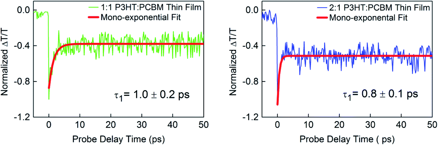 | ||
| Fig. 2 Normalized differential probe pulse transmission dynamics ΔT/T showing photoinduced transient absorption at 638 nm in P3HT:PCBM thin films with weight ratios 1:1 and 2:1 using 12 μJ cm−2 initial pump pulse excitation at 520 nm. | ||
| Excitation fluence | Reverse bias (V) | t1 (ps) | A1 (%) | Y0 (%) |
|---|---|---|---|---|
Dynamics in 1![[thin space (1/6-em)]](https://www.rsc.org/images/entities/b_char_2009.gif) :1 P3HT:PCBM device (mono-exponential fit)b :1 P3HT:PCBM device (mono-exponential fit)b |
||||
| 12 μJ cm−2 | 0 | 1.7 ± 0.1 | 65.07 ± 0.04 | 34.93 ± 0.05 |
| −1 | 1.3 ± 0.1 | 66.22 ± 0.02 | 33.78 ± 0.04 | |
| −2 | 1.1 ± 0.1 | 69.31 ± 0.03 | 30.69 ± 0.03 | |
| 24 μJ cm−2 | 0 | 1.3 ± 0.1 | 69.90 ± 0.01 | 30.100 ± 0.007 |
| −1 | 0.9 ± 0.1 | 63.56 ± 0.02 | 36.440 ± 0.003 | |
| −2 | 0.8 ± 0.1 | 62.18 ± 0.02 | 37.820 ± 0.001 | |
|
||||
| Dynamics in 2:1 P3HT:PCBM device (mono-exponential fit)b |
||||
| 12 μJ cm−2 | 0 | 2.1 ± 0.1 | 65.11 ± 0.04 | 34.89 ± 0.05 |
| −0.5 | 1.5 ± 0.2 | 64.81 ± 0.03 | 35.19 ± 0.02 | |
| −1 | 1.1 ± 0.1 | 65.55 ± 0.02 | 34.45 ± 0.04 | |
| −2 | 0.9 ± 0.1 | 69.01 ± 0.03 | 30.99 ± 0.03 | |
| 24 μJ cm−2 | 0 | 1.8 ± 0.07 | 67.01 ± 0.01 | 32.99 ± 0.02 |
| −0.5 | 1.3 ± 0.06 | 68.81 ± 0.02 | 31.19 ± 0.02 | |
| −1 | 1.0 ± 0.07 | 63.56 ± 0.01 | 36.44 ± 0.01 | |
| −2 | 0.8 ± 0.08 | 65.11 ± 0.03 | 35.89 ± 0.05 | |
| Dynamics in P3HT:PCBM devices in forward bias (mono-exponential fit)b | ||||
|---|---|---|---|---|
| Excitation fluence | Composition/forward bias (V) | t1 (ps) | A1 (%) | Y0 (%) |
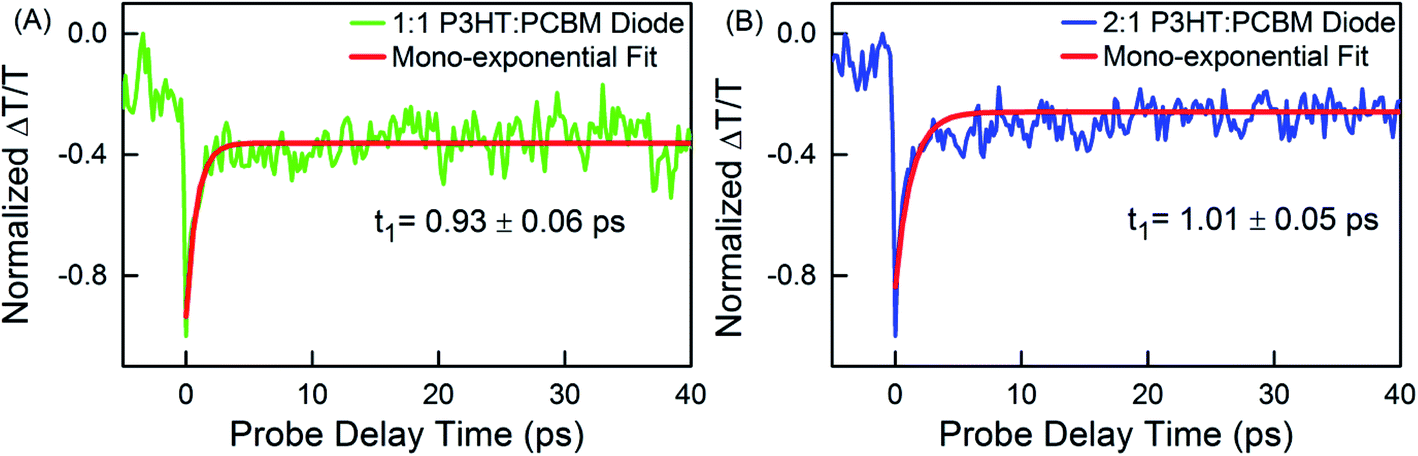
| 24 μJ cm−2 | 1:1/0.71 |
0.93 ± 0.06 | 64.23 ± 0.4 | 35.67 ± 0.4 |
| 2:1/0.73 |
1.01 ± 0.15 | 65.78 ± 0.2 | 34.22 ± 0.2 | |
3.2 Photoinduced absorption dynamics in P3HT:PCBM solar cell devices
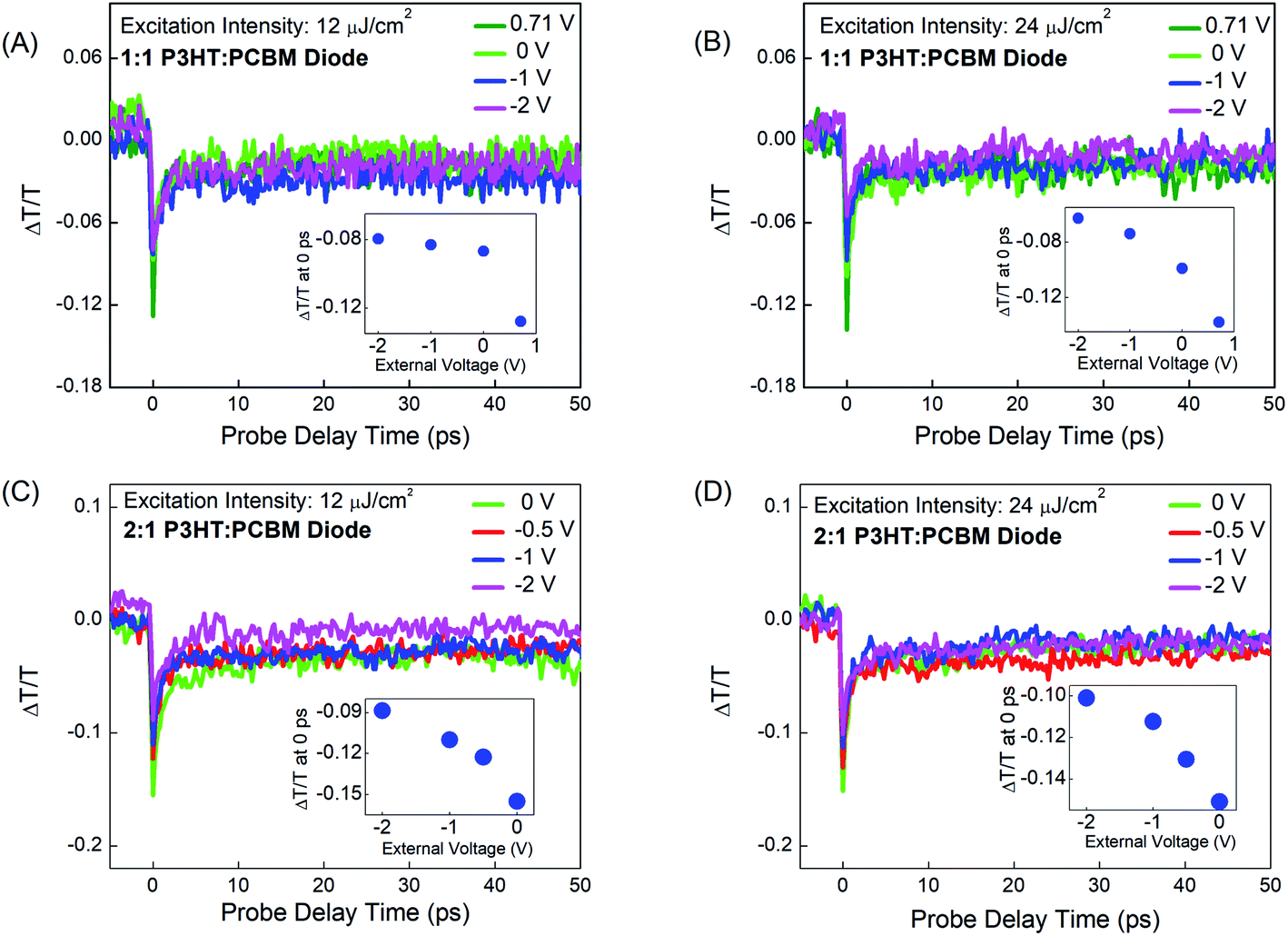
The main goal of this work is to investigate the PA dynamics at the 650 nm band in P3HT:PCBM devices under the influence of a static external electric field. This investigation helps to gain more information about the elementary processes occurring in organic semiconductor devices under operation. For the investigation, devices in a typical solar-cell configuration were fabricated as described in the experimental section. The P3HT:PCBM blend forming the active layer in the devices is exactly the same as the above mentioned thin P3HT:PCBM film deposited on a glass substrate.Panels (A) and (B) of Fig. 3 show the PA dynamics in a P3HT:PCBM device with 1:1 weight ratio for excitation intensities 12 and 24 μJ cm−2, respectively, observed for varying applied biases. The corresponding dynamics in a 2:1 P3HT:PCBM device are shown in panels (C) and (D) of Fig. 3. The applied voltages were 0, −1, and −2 V in reverse bias; an additional reverse bias voltage value of −0.5 V was applied to the 2:1 P3HT:PCBM device. The resulting net-electric fields, which are a function of the total voltage across each device and the film thickness, were 0.0355 MV cm−1 due to the built-in potential of −0.71 V in the 1:1 P3HT:PCBM device, 0.0365 MV cm−1 due to the built-in potential of −0.73 V in the 2:1 P3HT:PCBM device and 0.0615, 0.0855, and 0.1355 MV cm−1 due to the applied external reverse bias voltages of −0.5, −1, and −2 V, respectively. Additionally, in order to compensate the internal fields due to the diode arrangement, 0.71 and 0.73 V were applied in forward bias to the 1:1 and 2:1 P3HT:PCBM devices, respectively, resulting in an approximate field-free condition.
 | ||
| Fig. 3 Differential probe pulse transmission dynamics ΔT/T showing photoinduced transient absorption at 638 nm in 1:1 (top panels) and 2:1 (bottom panels) P3HT:PCBM solar cell devices after initial pump pule excitation fluences of 12 (left panels) and 24 μJ cm−2 (right panels) and for different applied voltages. | ||
In comparison to the results obtained from the P3HT:PCBM thin films, different dynamics can be observed for the P3HT:PCBM devices. The insets in Fig. 3 show the field-induced quenching of the PA at 0 ps. This quenching is due to the immediate loss of photoexcitation species because of field-induced dissociation. For a better illustration of the field-induced quenching, we have included the PA decay for the field-free case, in which the appropriate forward bias was applied to compensate the built-in field in the devices. The PA quenching appears to be less sensitive to the applied external fields in the P3HT:PCBM with a higher PCBM content. This is consistent with the fact that the presence of the PCBM acceptor should result in primary photoexcitation species with a significant fraction of dissociative states such as CT excitons, which can dissociate on an ultrashort time scale already in the absence of the externally applied field.
Similar to the case of P3HT:PCBM thin films, the overall decay dynamics patterns detected for the different excitation fluences in the 1:1 and 2:1 P3HT:PCBM devices could be fitted using mono-exponential decay functions with a time constant t1. Only for the measurement at the higher fluence in the 2:1 device, we found that a bi-exponential fitting was slightly more precise in theory; however, while this added only a minor additional component to the PA dynamics, it did not result in an overall unambiguous picture and an explanation would have required even further higher-excitation-fluence data not achievable due to sample damage. Hence, a mono-exponential fitting model has been presented, since it still helps to capture the overall dominant trend of the PA dynamics in this case as well like for all other cases. The fitting curves are shown in Fig. S4–S7 in the ESI,† and the fitting parameters are included in Table 1.
Compared to P3HT:PCBM thin films, overall slower PA dynamics are observed at the 650 nm PA band in the P3HT:PCBM devices with zero external bias, i.e. when only the built-in potential is present. Consistent with our previous study on a P3HT-only diode,35 the measured dynamics become faster with increasing external electric fields applied in reverse bias, suggesting that the electric field is supporting the gradual dissociation of bound charge-pair species. On this basis and given the well-established contribution of PPs to the 650 nm PA in P3HT thin films, the assumption that PPs are also formed in P3HT:PCBM after photoexcitation appears to be rather plausible. In this connection, the ultraslow decay component approximated by an offset in the fitted dynamics for the P3HT:PCBM thin film and devices can be assigned to long-lived species such as 2D delocalized polarons, in agreement with previous studies.35,49
The general understanding is that the exciton dissociation happens via intermediate steps by forming CT states at the donor–acceptor interface.33,46 In our earlier study we introduced the concept of a field-induced diffusion-controlled slower generation of PPs from excitons in P3HT-only diodes, resulting in complex PP dynamics with an additional significantly slower component besides an ultrafast component assigned to the nascent PPs formed on an ultrashort time scale. In the present study, we show that this field-induced exciton dissociation process appears to be also responsible for the overall slow PA decay in the P3HT:PCBM devices observed when probing within the 650 nm PA band.
Firstly, the PA dynamics patterns at low excitation intensity in P3HT:PCBM devices seemingly do not show a separate ultrafast component typical of the so-called nascent PPs discussed in the case of P3HT and 1:1 and 2:1 P3HT:PCBM thin films. This may be due to the combined effect of (i) efficient CT exciton formation competing with PP generation in these donor–acceptor systems and (ii) ultrafast field-induced dissociation of intermediate charge-pair species at early time scales. Secondly, because an efficient formation of the highly dissociative CT excitons also leads to the reduction of thermalized excitons, the field-induced generation of PPs from these thermalized excitons occurs during a shorter time in comparison to the situation in the P3HT-only device where a negligible fraction of CT excitons is expected. This is also supported by the observation that compared to the 1:1 P3HT:PCBM device, for lower excitation intensity, we find a slower PA decay in the 2:1 P3HT:PCBM device. This can be explained by a higher proportion of CT excitons due to the presence of more donor/acceptor interfacial regions in the 1:1 P3HT:PCBM device.
We can conclude that the detected PA dynamics are dominated by a field-induced regeneration of intermediate charge-pair species, which however lasts a relatively short time (overall decay time only about 2 ps) in P3HT:PCBM devices as compared to the P3HT-only device for low excitation fluence. In a realistic organic semiconductor device like the investigated P3HT:PCBM system, where the combined effect of the acceptor (for efficient formation of the highly dissociative CT excitons) and an applied external electric field is expected to result in optimal charge separation, it is of significant relevance that a field-mediated formation of loosely bound intermediate states persists (PP states in this case). The significance of this observation is further illustrated in the dynamics obtained at higher excitation fluence.
Comparing panels (A) and (B) of Fig. 3 shows that the measured PA decay dynamics are getting faster with the increase in excitation intensity for the 1:1 P3HT:PCBM device (see Table 1 for fitting parameters). This intensity-dependent behavior can be attributed to a bimolecular annihilation process, which represents a charge-loss pathway reflected in the intermediate charge-pair species being formed in P3HT:PCBM devices under the effect of static electric fields. The bimolecular process could happen due to both exciton–exciton annihilation or exciton-charge annihilation processes.50 Given the observations in previous studies pointing to the possibility of exciton–exciton annihilation at rather low excitation fluences (e.g. 3 μJ cm−2),30,31 the pump excitation intensity used for our measurements is sufficiently high for initiating bimolecular processes for the primary excitation species (excitons) even when the smaller fluence is chosen (12 μJ cm−2). The PP absorption following the initial photoexcitation process is rather weak in P3HT:PCBM thin films, which justifies the use of somewhat higher laser intensities. However, one also has to consider that only part of the laser intensity will interact with the active semiconductor layer in the investigated P3HT:PCBM devices since the Ag layer used as the contact electrode reflects some light. For the higher excitation fluence, we also find that the overall PA dynamics in the 1:1 P3HT:PCBM device become less affected by applied fields corresponding to external voltages beyond ∼1 V. This may be because of (i) field-induced PP conversion into low-dipole-moment species with similar PA beyond a given external field threshold in both devices and (ii) comparable rates for field-induced PP generation (via exciton dissociation) and field-induced PP dissociation in the 1:1 device. While – as already pointed out above – the overall decay times become longer for the 2:1 P3HT:PCBM device compared to the 1:1 device, the intensity-dependent behavior is comparable to that observed for the 1:1 device (see panels (C) and (D) of Fig. 3 and Table 1).
Altogether, the static electric field effects play a rather decisive role for the PP dynamics observed in the P3HT:PCBM devices, as further illustrated below by the measurements performed on the forward-based devices.
In the experiments already discussed above, it was noted that the P3HT:PCBM devices fabricated with different P3HT:PCBM weight ratios have an internal built-in potential due to the different work functions of the materials used as contacts to the organic layer stack of each device. The built-in potentials of the devices are −0.71 and −0.73 V for P3HT:PCBM weight ratios of 1:1 and 2:1, respectively. As discussed above, a field-induced effect on the measured PA dynamics is already observed at 0 V external bias, i.e., when only the built-in potential is present. In order to approximately eliminate the field-induced effects caused by this built-in-potential, we have operated each of the devices with a compensating externally applied forward bias. Fig. 4 shows the dynamics obtained at the same probe wavelength under these conditions at 24 μJ cm−2. Like already observed for the thin films, a mono-exponential decay function was sufficient to fit the dynamics. This yields a fast decay for both devices (time constant t1), which is comparable to that observed for the field-free thin-film case (time constant τ1), and the dynamics in this case are less dependent on the pump laser intensity (shown in Fig. S8†). This strongly supports our assumption that the changes observed in the measured dynamics in the reverse biased devices (with net non-zero static electric field) compared to the thin film results are the consequence of the electric field-induced effects, which we have already explained above. This field-induced component gets faster with increasing reverse bias, resulting in an overall time constant, which for high reverse bias values again comes closer to the values observed in the thin film samples.
 | ||
| Fig. 4 Differential probe transmission dynamics ΔT/T showing photoinduced transient absorption at 638 nm in 1:1 (A) and 2:1 (B) P3HT:PCBM solar cell devices under a forward bias compensating the built-in potential after initial pump pulse excitation with 24 μJ cm−2. | ||
3.3 Transient absorption anisotropy in P3HT:PCBM thin films and solar cell devices
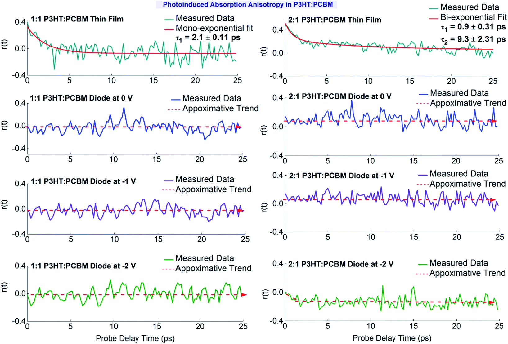
In order to gain more information about the effect of electric fields on the PA dynamics measured at 638 nm in P3HT:PCBM systems, we have carried out transient pump–probe anisotropy measurements in resonance (i.e. absorption anisotropy). The higher pump fluence of 24 μJ cm−2 was used for better signal-to-noise ratio. The PA anisotropy r(t) has been calculated using the following equation:where (ΔT/T)‖ and (ΔT/T)⊥ are the differential probe pulse transmissions for the probe pulse polarization parallel and perpendicular to that of the pump pulse, respectively.51–53 In these experiments, pump and probe lasers were entering the sample perpendicularly to the electrode surface. For the change of the relative polarization, the pump pulse polarization was rotated, while the probe pulse polarization was kept constant. Fig. 5 shows the measured anisotropy decay of the PA detected at 638 nm in P3HT:PCBM thin films and devices. In the case of 1
 :1 P3HT:PCBM thin film, the anisotropy is about 0.40 ± 0.01 at time zero and then quickly decays to zero over time. The pump pulse creates an excitation polarization for the exited state species, which can efficiently couple to the probe pulse light field when these two pulses have parallel polarizations. The fast anisotropy decay suggests that the absorbing species quickly loose the initial polarization information. Different processes might contribute to this behavior. Among others, the fast transition from higher to lower energy dissociation sites due to the high mobility of the PPs would explain the rapid loss of the polarization memory. The anisotropy decay has been fitted with a mono-exponential decay function, which gives a decay time constant of t1 = 2.1 ± 0.1 ps. This result is interesting since we have already discussed (see Fig. 2) that the lifetime of the PPs observed in the 1:1 P3HT:PCBM thin film is approximately 1 ps. Let's recall that all other PA transients correspond to parallel pump and probe polarizations. Hence, the longer lifetime of the polarization memory suggests the presence of different other species observed at the probe wavelength. The high anisotropy value at 0 ps (r(0) = 0.40 ± 0.01) in 1:1 P3HT:PCBM thin film points to the fact that the photoexcited species absorbing in the 650 nm band are rather stable bound species. This indicates that the observed transient absorption signal is most probably dominated by contributions due to PPs. A similar observation is seen in the PA anisotropy for the 2:1 P3HT:PCBM thin film.
 | ||
| Fig. 5 Pump–probe anisotropy decay dynamics in P3HT:PCBM thin films and solar cell devices with different weight ratios of 1:1 (left panels) and 2:1 (right panels) at 638 nm probe pulse after an initial pump excitation with 24 μJ cm−2 fluence. Data for devices taken for various external reverse biases. | ||
In the case of 2:1 P3HT:PCBM thin film, the initial anisotropy at 0 ps is 0.46 ± 0.02, which is slightly higher than the value obtained for the 1.1 P3HT:PCBM thin film (the fact that this value slightly exceeds the fundamental anisotropy value of 0.4,54 can be attributed to the relatively poor signal to noise ratio). In addition, the anisotropy decay pattern is different, showing much slower decay dynamics. A slow decay channel starts to contribute noticeably also to the polarization memory loss in the 2:1 P3HT:PCBM thin film. Because the change in anisotropy is driven by local structural details, we can attribute the existence of both rapid and slower anisotropy dynamics to structurally different species due to morphological differences in the two P3HT:PCBM films, which differ in their relative mass contents. However, overlapping contributions from different species37,55 complicate the interpretation of the anisotropy results.
Fig. 5 also shows the transient anisotropy decay patterns obtained from the P3HT:PCBM solar cell devices for different applied external electric fields. In general, we observe no noticeable anisotropy for the 1:1 P3HT:PCBM device and only a very weak anisotropy for the 2:1 P3HT:PCBM device in the reverse-bias case. These results are a further evidence for the strong effect of the static electric field on the PPs and their precursor species. These findings might be a clear manifestation of the field-induced dissociation processes, occurring and saturating with the built-in potential present in the device. While for the 1:1 P3HT:PCBM device we cannot recognize any anisotropy effect, a very small anisotropy can be observed for the 2:1 device. This agrees with the explanation that we have provided about the difference in the PP dynamics for the two devices, assuming that the fraction of interfacial CT excitons, which can quickly dissociate even without additional electric field, is higher in the 1:1 device, resulting in a rapid reduction in the amount of PP precursors. For 0 V (only built-in potential present) and 1 V reverse bias in the case of the 2:1 device, we find a small positive anisotropy, which is constant on the observed timescale. However, after increasing the external reverse bias to −2 V, a decay pattern can be recognized for the anisotropy. Interestingly, now at time zero no anisotropy can be detected, while from there a negative value for the anisotropy develops. A negative anisotropy indicates that the transition dipole moment for the absorption of the probe pulse polarized perpendicularly to the initial pump pulse polarization is dominant. Again, the donor–acceptor weight ratio used to prepare the P3HT:PCBM devices has a noticeable influence on the anisotropy dynamics observed.
While in the films, the anisotropy is expected to be mainly induced by the electric field of the pump laser pulse resulting in an initial positive value, which then decays due to the decay of the absorbing species and the loss of the orientation of this species, the situation for the devices is different. Here, the externally applied and the built-in electric fields provide re-orientational forces and additionally contribute to the dissociation process. In this connection, for 1:1 P3HT:PCBM, the donor–acceptor interfaces in the heterostructure and the species formed at these interfaces are actually more in proportion than for the 2:1 mixture and a more efficient generation of charges is also expected there. These differences might explain the different behavior for the 2:1 P3HT:PCBM. However, a detailed explanation is not possible based on the available data and we cannot present a model, which e.g. explains the strange behavior seen for the 2:1 P3HT:PCBM device at −2 V applied reverse bias. Further investigations e.g. looking simultaneously for the contribution of other species will be helpful, which are not possible with our present experimental setup.
3.4 Physical processes affecting photoinduced absorption dynamics in 1![[thin space (1/6-em)]](https://www.rsc.org/images/entities/h3_char_2009.gif) :1 and 2:1 P3HT:PCBM solar cell devices
:1 and 2:1 P3HT:PCBM solar cell devices
Fig. 6 schematically summarizes the physical processes influencing the dynamics of the 650 nm PA band measured at 12 and 24 μJ cm−2 pump pulse excitation fluences in presence of an applied external electric field in the 1:1 and 2:1 P3HT:PCBM solar cell devices. The primary physical process involves the formation of hot excitons from the ground state (curvy black line), followed by an ultrafast formation of intermediate charge-pair states from these hot excitons within less than 100 fs (shown by the solid black line).56,57 Based on a comparison with earlier results on P3HT films and devices,32 we tentatively assign the main contribution in our probed spectral window to PPs. Also, charge-transfer excitons (CT) are rapidly and efficiently formed in the P3HT:PCBM donor–acceptor system. The solid grey lines depict the generation of thermalized singlet excitons (S1), charge-transfer excitons (CT), and polaron states from the hot excitons. The PP state can gain energy from (i) thermal perturbations available in the system after hot-exciton generation, and (ii) both internal and external electric fields in the case of a field-induced PP generation process; however the actual relative position of this state in the energy scale depends on other factors such the structural stabilization energy. For this reason, the presented scheme is not to scale. In our experiments, we focus on the PP generation and decay mechanisms. τ1 represents for the P3HT:PCBM devices the uni-molecular decay of PPs, which generally occur in thin films and shows no excitation intensity dependence (so, for forward-biased devices whose PA dynamics, as already explained, closely resemble that of the thin films, the τ1 time constant is nothing else but t1 shown for this case in Table 1). This decay contribution was not separately estimated as it is overlaid by further processes in the P3HT:PCBM devices due to (i) efficient CT exciton formation competing with PP generation and (ii) ultrafast field-induced PP dissociation at early time scales. The time constant t1 for the P3HT:PCBM devices represents the dynamics of PPs resulting in polarons including field-induced effects. The time constant extracted from the mono-exponential fit represents all possible decay channels affecting the PPs not only in the devices but also in the thin films and is therefore an approximation of t1 (or τ1), which however might be a dominating factor. Long-lived states (LLS, represented by the offset of the exponentially fitted dynamics Y0) are usually present along with the PP states.
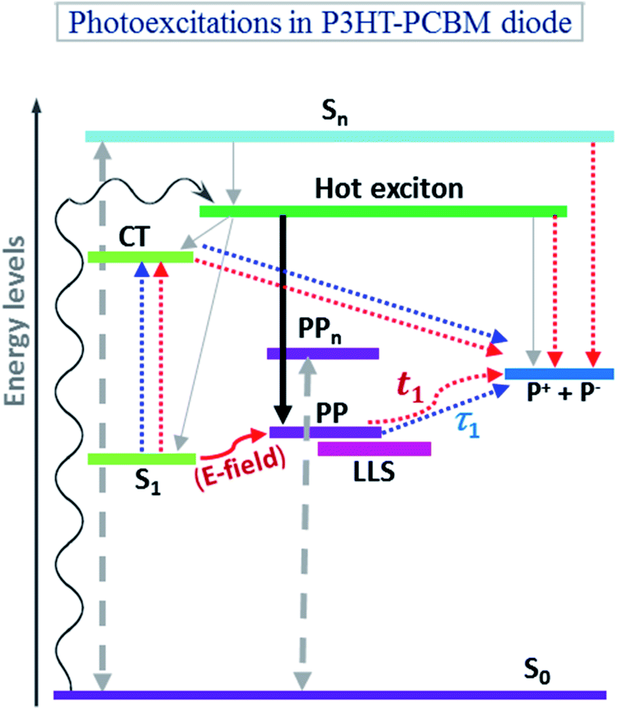 | ||
| Fig. 6 Schematic energy diagram (not to scale) depicting physical processes contributing to the dynamics of photoinduced absorption measured at 638 nm in 1:1 and 2:1 P3HT:PCBM solar cell devices under the influence of applied electric fields for 12 and 24 μJ cm−2 initial pump pulse (520 nm) excitation fluence. S0: electronic ground state; S1: (thermalized) singlet exciton; Sn: high-energy exciton; CT: charge transfer exciton; PP: polaron-pair; LLS: long lived states; PPn: high-energy PP state; P+ + P−: polaron states. Black line: ultrafast formation of nascent PPs; dotted blue lines: pump-initiated processes without electric field; dashed grey lines: bimolecular annihilation processes; red lines: electric-field-influenced processes; τ1: PP decay in the absence of any electric field; t1: PP decay occurring with the influence of an electric field. The energy levels given are only schematic and the energy scale is therefore not reflecting quantitative values. See text for more details. | ||
The presence of an overall non-zero net electric field (external + built-in field) results in an ultrafast dissociation of several electron–hole-pair species including thermalized excitons (i.e. singlet-exciton state S1), CT excitons, hot excitons, etc.; in Fig. 6, these dissociation processes are indicated by red dotted lines (not shown from S1 for the sake of clarity). In addition, a diffusion-controlled field-mediated singlet-exciton dissociation process populates the PP state as depicted by the solid red line. This process results in overall slower PP dynamics. In the investigated P3HT:PCBM devices, the duration of this generation process is shortened by the fact that the rapid formation of CT excitons, which are highly dissociative in nature, causes the proportion of the precursor excitons (S1) to be already reduced at the early time scales. Bimolecular annihilation processes shown by two-sided grey arrow lines have also been observed on the PP dynamics. The PP dynamics in the P3HT:PCBM devices are field-dependent and show a decay time t1, which is slower than that observed in the thin films or in the devices where an external forward bias compensates the internal field. Increasing the excitation light fluence results in faster decay dynamics due to the contribution of bimolecular decay processes.
4 Conclusions
We have performed femtosecond time-resolved transient absorption spectroscopy measurements using 520 nm pump and 638 nm probe pulses in order to investigate the effect of static electric fields on the photoinduced absorption dynamics in P3HT:PCBM systems. To this end, P3HT:PCBM thin films with 1:1 and 2:1 weight ratios deposited on glass substrates were used as reference for measurements without any electric field. Diode-like devices made from these films in a typical layer stack solar cell configuration were then employed for electric field-dependent measurements both in reverse bias resulting in electric fields influencing the charge-pair dynamics and in forward bias compensating the built-in potential of the devices. In addition, PA anisotropy measurements have been performed in order to study the effect of the sample morphology.
By comparing the dynamics obtained from thin films to that obtained from the respective devices, we have shown that the field-induced dissociation of singlet excitons affects the population of the probed transient state, resulting in comparatively slower decay dynamics. The external electric field is expected to generate polarons by dissociating not only excitons and PPs, but also CT excitons immediately since the latter can dissociate on an ultrashort time scale near the donor–acceptor interface without the need for external electric fields. Interestingly however, even though an efficient formation of CT excitons is expected to result in an overall seamless dissociation process, the present results demonstrate that during the exciton dissociation induced by static electric fields in the P3HT:PCBM devices (built-in and/or externally added fields), additional intermediate charge-pair species are formed as transient states of the semiconductor system. Based on a comparison to our earlier studies on P3HT thin films and diodes, we have tentatively assigned this intermediate state detected by our probe laser pulse to PPs. Furthermore, an increase of the photoexcitation intensity results in bimolecular annihilation processes contributing as additional loss channel reflected by faster PP dynamics. As compared to the 1:1 P3HT:PCBM device, the effect of externally applied electric fields has been found to be more pronounced in the 2:1 P3HT:PCBM device, where the proportion of CT excitons is relatively smaller.
The experiments using pump and probe laser pulses with different relative polarization directions (parallel and orthogonal) yielded the PP anisotropy dynamics. While the 1:1 P3HT:PCBM thin film shows a fast PP anisotropy decay with a time constant of ∼2 ps, the 2:1 thin film shows an overall much slower decay component (∼9 ps). The 1:1 P3HT:PCBM device shows no PP anisotropy, while for the 2:1 P3HT:PCBM device we observe a very small positive constant anisotropy for small reverse bias and anisotropy values developing from zero at time zero to a negative value over time for lager reverse bias (−2 V).
Future experiments not currently feasible with our present setup will be required to develop a more detailed model of the involved dynamical processes for the P3HT:PCBM device under the influence of static electric fields and to explain the negative PP anisotropy observed for large reverse bias in the 2:1 device.
Conflicts of interest
There are no conflicts of interest to declare.References
- G. Yu, J. Gao, J. C. Hummelen, F. Wudl and A. J. Heeger, Science, 1995, 270, 1789–1791 CrossRef CAS.
- Y. Yang, Z.-G. Zhang, H. Bin, S. Chen, L. Gao, L. Xue, C. Yang and Y. Li, J. Am. Chem. Soc., 2016, 138, 15011–15018 CrossRef CAS.
- H. Hu, K. Jiang, G. Yang, J. Liu, Z. Li, H. Lin, Y. Liu, J. Zhao, J. Zhang and F. Huang, J. Am. Chem. Soc., 2015, 137, 14149–14157 CrossRef CAS.
- Z. Li, K. Jiang, G. Yang, J. Y. L. Lai, T. Ma, J. Zhao, W. Ma and H. Yan, Nat. Commun., 2016, 7, 1–9 Search PubMed.
- W. Zhao, S. Li, H. Yao, S. Zhang, Y. Zhang, B. Yang and J. Hou, J. Am. Chem. Soc., 2017, 139, 7148–7151 CrossRef CAS.
- S. Zhang, Y. Qin, J. Zhu and J. Hou, Adv. Mater., 2018, 30, 1800868 CrossRef.
- Z. Zheng, O. M. Awartani, B. Gautam, D. Liu, Y. Qin, W. Li, A. Bataller, K. Gundogdu, H. Ade and J. Hou, Adv. Mater., 2017, 29, 1604241 CrossRef.
- D. A. Vithanage, A. Devižis, V. Abramavičius, Y. Infahsaeng, D. Abramavičius, R. MacKenzie, P. Keivanidis, A. Yartsev, D. Hertel and J. Nelson, Nat. Commun., 2013, 4, 1–6 Search PubMed.
- F. Gao and O. Inganäs, Phys. Chem. Chem. Phys., 2014, 16, 20291–20304 RSC.
- S. Athanasopoulos, S. Tscheuschner, H. Bässler and A. Köhler, J. Phys. Chem. Lett., 2017, 8, 2093–2098 CrossRef CAS.
- J. Lee, K. Vandewal, S. R. Yost, M. E. Bahlke, L. Goris, M. A. Baldo, J. V. Manca and T. Van Voorhis, J. Am. Chem. Soc., 2010, 132, 11878–11880 CrossRef CAS.
- A. A. Bakulin, A. Rao, V. G. Pavelyev, P. H. van Loosdrecht, M. S. Pshenichnikov, D. Niedzialek, J. Cornil, D. Beljonne and R. H. Friend, Science, 2012, 335, 1340–1344 CrossRef CAS.
- A. A. Bakulin, S. D. Dimitrov, A. Rao, P. C. Chow, C. B. Nielsen, B. C. Schroeder, I. McCulloch, H. J. Bakker, J. R. Durrant and R. H. Friend, J. Phys. Chem. Lett., 2013, 4, 209–215 CrossRef CAS.
- K. Tvingstedt, K. Vandewal, A. Gadisa, F. Zhang, J. Manca and O. Inganas, J. Am. Chem. Soc., 2009, 131, 11819–11824 CrossRef CAS.
- S. K. Pal, T. Kesti, M. Maiti, F. Zhang, O. Inganas, S. Hellstrom, M. R. Andersson, F. Oswald, F. Langa and T. Osterman, J. Am. Chem. Soc., 2010, 132, 12440–12451 CrossRef CAS.
- J. D. Lin, O. V. Mikhnenko, J. Chen, Z. Masri, A. Ruseckas, A. Mikhailovsky, R. P. Raab, J. Liu, P. W. Blom and M. A. Loi, Mater. Horiz., 2014, 1, 280–285 RSC.
- Y. Tamai, H. Ohkita, H. Benten and S. Ito, J. Phys. Chem. Lett., 2015, 6, 3417–3428 CrossRef CAS.
- S. Shoaee, S. Subramaniyan, H. Xin, C. Keiderling, P. S. Tuladhar, F. Jamieson, S. A. Jenekhe and J. R. Durrant, Adv. Funct. Mater., 2013, 23, 3286–3298 CrossRef CAS.
- F. C. Jamieson, E. B. Domingo, T. McCarthy-Ward, M. Heeney, N. Stingelin and J. R. Durrant, Chem. Sci., 2012, 3, 485–492 RSC.
- N. Grossiord, J. M. Kroon, R. Andriessen and P. W. Blom, Org. Electron., 2012, 13, 432–456 CrossRef CAS.
- V. Jovanov, N. Yumnam, A. Müller, M. Gruber and V. Wagner, J. Phys. Chem. C, 2017, 121, 9173–9180 CrossRef CAS.
- D. W. Gehrig, I. A. Howard, S. Sweetnam, T. M. Burke, M. D. McGehee and F. Laquai, Macromol. Rapid Commun., 2015, 36, 1054–1060 CrossRef CAS.
- B. M. Savoie, A. Rao, A. A. Bakulin, S. Gelinas, B. Movaghar, R. H. Friend, T. J. Marks and M. A. Ratner, J. Am. Chem. Soc., 2014, 136, 2876–2884 CrossRef CAS.
- T. M. Burke and M. D. McGehee, Adv. Mater., 2014, 26, 1923–1928 CrossRef CAS.
- A. A. Guilbert, M. Schmidt, A. Bruno, J. Yao, S. King, S. M. Tuladhar, T. Kirchartz, M. I. Alonso, A. R. Goñi and N. Stingelin, Adv. Funct. Mater., 2014, 24, 6972–6980 CrossRef CAS.
- L. W. Barbour, M. Hegadorn and J. B. Asbury, J. Am. Chem. Soc., 2007, 129, 15884–15894 CrossRef CAS.
- J. Piris, T. E. Dykstra, A. A. Bakulin, P. H. v. Loosdrecht, W. Knulst, M. T. Trinh, J. M. Schins and L. D. Siebbeles, J. Phys. Chem. C, 2009, 113, 14500–14506 CrossRef CAS.
- S. Cook, R. Katoh and A. Furube, J. Phys. Chem. C, 2009, 113, 2547–2552 CrossRef CAS.
- R. A. Marsh, J. M. Hodgkiss, S. Albert-Seifried and R. H. Friend, Nano Lett., 2010, 10, 923–930 CrossRef CAS.
- J. Guo, H. Ohkita, H. Benten and S. Ito, J. Am. Chem. Soc., 2010, 132, 6154–6164 CrossRef CAS.
- J. Guo, H. Ohkita, H. Benten and S. Ito, J. Am. Chem. Soc., 2009, 131, 16869–16880 CrossRef CAS.
- A. R. S. Kandada, G. Grancini, A. Petrozza, S. Perissinotto, D. Fazzi, S. S. K. Raavi and G. Lanzani, Sci. Rep., 2013, 3, 2073 CrossRef.
- G. Grancini, D. Polli, D. Fazzi, J. Cabanillas-Gonzalez, G. Cerullo and G. Lanzani, J. Phys. Chem. Lett., 2011, 2, 1099–1105 CrossRef CAS.
- E. Lioudakis, I. Alexandrou and A. Othonos, Nanoscale Res. Lett., 2009, 4, 1475 CrossRef CAS.
- D. Rana, P. Donfack, V. Jovanov, V. Wagner and A. Materny, Phys. Chem. Chem. Phys., 2019, 21, 21236–21248 RSC.
- A. De Sio, F. Troiani, M. Maiuri, J. Réhault, E. Sommer, J. Lim, S. F. Huelga, M. B. Plenio, C. A. Rozzi and G. Cerullo, Nat. Commun., 2016, 7, 1–8 Search PubMed.
- O. G. Reid, R. D. Pensack, Y. Song, G. D. Scholes and G. Rumbles, Chem. Mater., 2014, 26, 561–575 CrossRef CAS.
- B.-R. Gao, H.-Y. Wang, H. Wang, Z.-Y. Yang, L. Wang, Y. Jiang, Y.-W. Hao, Q.-D. Chen and H.-B. Sun, IEEE J. Quantum Electron., 2011, 48, 425–432 Search PubMed.
- M. Menšík, J. Pfleger and P. Toman, Chem. Phys. Lett., 2017, 677, 87–91 CrossRef.
- R. Marsh, C. McNeill, A. Abrusci, A. Campbell and R. H. Friend, Nano Lett., 2008, 8, 1393–1398 CrossRef CAS.
- A. R. Campbell, J. M. Hodgkiss, S. Westenhoff, I. A. Howard, R. A. Marsh, C. R. McNeill, R. H. Friend and N. C. Greenham, Nano Lett., 2008, 8, 3942–3947 CrossRef CAS.
- V. D. Mihailetchi, H. Xie, B. de Boer, L. A. Koster and P. W. Blom, Adv. Funct. Mater., 2006, 16, 699–708 CrossRef CAS.
- H. Bässler and A. Köhler, Phys. Chem. Chem. Phys., 2015, 17, 28451–28462 RSC.
- I.-W. Hwang, D. Moses and A. J. Heeger, J. Phys. Chem. C, 2008, 112, 4350–4354 CrossRef CAS.
- C. G. Shuttle, B. O'Regan, A. M. Ballantyne, J. Nelson, D. D. Bradley and J. R. Durrant, Phys. Rev. B: Condens. Matter Mater. Phys., 2008, 78, 113201 CrossRef.
- H. Ohkita, S. Cook, Y. Astuti, W. Duffy, S. Tierney, W. Zhang, M. Heeney, I. McCulloch, J. Nelson and D. D. Bradley, J. Am. Chem. Soc., 2008, 130, 3030–3042 CrossRef CAS.
- R. A. Marsh, J. M. Hodgkiss and R. H. Friend, Adv. Mater., 2010, 22, 3672–3676 CrossRef CAS.
- A. Solanki, A. Bagui, G. Long, B. Wu, T. Salim, Y. Chen, Y. M. Lam and T. C. Sum, ACS Appl. Mater. Interfaces, 2016, 8, 32282–32291 CrossRef CAS.
- R. Österbacka, C. P. An, X. Jiang and Z. V. Vardeny, Science, 2000, 287, 839–842 CrossRef.
- J. M. Hodgkiss, S. Albert-Seifried, A. Rao, A. J. Barker, A. R. Campbell, R. A. Marsh and R. H. Friend, Adv. Funct. Mater., 2012, 22, 1567–1577 CrossRef CAS.
- E. Collini and G. D. Scholes, Science, 2009, 323, 369–373 CrossRef CAS.
- M.-L. Grage, P. Wood, A. Ruseckas, T. Pullerits, W. Mitchell, P. Burn, I. Samuel and V. Sundström, J. Chem. Phys., 2003, 118, 7644–7650 CrossRef CAS.
- S. Westenhoff, W. J. Beenken, R. H. Friend, N. C. Greenham, A. Yartsev and V. Sundström, Phys. Rev. Lett., 2006, 97, 166804 CrossRef.
- I. Hwang and G. D. Scholes, Chem. Mater., 2011, 23, 610–620 CrossRef CAS.
- D. M. Jonas, M. J. Lang, Y. Nagasawa, T. Joo and G. R. Fleming, J. Phys. Chem., 1996, 100, 12660–12673 CrossRef CAS.
- D. Moses, A. Dogariu and A. J. Heeger, Phys. Rev. B: Condens. Matter Mater. Phys., 2000, 61, 9373 CrossRef CAS.
- K. Vandewal, S. Albrecht, E. T. Hoke, K. R. Graham, J. Widmer, J. D. Douglas, M. Schubert, W. R. Mateker, J. T. Bloking and G. F. Burkhard, Nat. Mater., 2014, 13, 63–68 CrossRef CAS.
Footnote |
| † Electronic supplementary information (ESI) available: Describes the UV-Vis absorption of the P3HT:PCBM thin films and P3HT:PCBM diodes, the current–voltage characteristics and the fitting of the photoinduced transient absorption data obtained from the P3HT:PCBM diodes as a function of the applied bias and the pump pulse intensity. See DOI: 10.1039/d0ra07935a |
| This journal is © The Royal Society of Chemistry 2020 |