
 Open Access Article
 This Open Access Article is licensed under a
 Creative Commons Attribution 3.0 Unported Licence
Stability study of organometal halide perovskite and its enhanced X-ray scintillation from the incorporation of anodic TiO2 nanotubes†
Hui Lia,
Zhenhua Chen *b,
Zhuocheng Sanga,
Xiangzhi Zhangb and
Yong Wangb
*b,
Zhuocheng Sanga,
Xiangzhi Zhangb and
Yong Wangb
aDepartment of Optoelectronic Science and Engineering, College of Science, Donghua University, Songjiang District, Shanghai 201620, China
bShanghai Synchrotron Radiation Facility (SSRF), Shanghai Advanced Research Institute, Chinese Academy of Sciences, Shanghai 201800, China. E-mail: chenzhenhua@zjlab.org.cn
First published on 8th December 2020
Abstract
Organometal halide perovskite-based optoelectronic devices are currently a hot research area owing to their unique properties, but widespread commercialization is plagued by their poor long-term stability. So far, the degradation mechanism of organometal halide perovskites is still indistinct due to limited real time systematic study. In this work, we in situ study the crystal evolution of an organometal halide perovskite CH3NH3PbI3, which is prepared on different kinds of framework substrates. Based on the in situ grazing incidence X-ray diffraction and X-ray near absorption edge spectrum, we observe the formation of some 2D networks of [PbI6]4− octahedra intermediates during CH3NH3PbI3 degradation in a moist environment at the early step of the degradation mechanism. We also show that the structural stability of CH3NH3PbI3 deposited anodic TiO2 nanotube substrates is relatively better than that of prepared perovskite on TiO2 nanoparticles in moisture. The confinement of the 3D [PbI6]4− octahedral crystal network probability reduces the ion migration by regular pores of crystalline TiO2 nanotubes, improving the stability of the organometal halide perovskite. Furthermore, the X-ray excited luminescence intensity of CH3NH3PbI3 fabricated on TiO2 nanotubes is boosted 88% compared with that of conventional TiO2 nanoparticle substrates, which demonstrates its potential application in scintillation detectors.
1. Introduction
Organometal halide perovskites, CH3NH3PbX3 (X = Cl, Br, I), have become a popular topic with regard to optoelectronic devices in recent years. These perovskite structured semiconductors have benefitted from unique properties, including suitable bandgaps,1,2 high absorption coefficients,3 long charge carrier diffusion lengths,4 and high carrier mobility with low recombination rate.5–7 The perovskites thus attract progressive attention for potential applications in fields such as solar cells,8–14 wavelength tunable light emitting diodes (LEDs),15–21 microlasers,22,23 X-ray photodetectors and scintillation.24–30Despite significant progress in organometal halide perovskite-based optoelectronic devices, widespread commercialization is plagued by their poor long-term stability. Because of the soft nature of organometal halide perovskites, perovskite devices are very sensitive to environmental factors such as light, heat and water vapor, which greatly reduce their working stability.12,31,32 Among these issues, moisture is one of the most important factors that rapidly degrades organometal halide perovskites, resulting in a significant decline in device performance.33 Yang et al. reported the photo conversion efficiency (PCE) dropped 80% over a 24 h period when the cells were stored under ambient conditions and a 95% drop in PCE after 6 days for unencapsulated perovskite solar cells.8 Seok et al. reported that CH3NH3PbI3 began to decompose under the condition of 50% humidity, and its color gradually changed from dark brown to yellow, accompanied by the degradation of the device efficiency.34 In organometal halide perovskite-based light emitting diodes (LEDs), the degradation of perovskites induces ion movement, resulting in structural distortion and luminescence wavelength shift, and the peak efficiency of perovskite LEDs is only seconds or minutes under operation.35
In the degradation study of organometal halide-based optoelectronics, Wang et al. reported that the combined action of water and oxygen led to irreversible decomposition of perovskites. Perovskite CH3NH3PbI3 is extremely sensitive to moisture, easily producing CH3NH2, HI, and PbI2 by hydrolyzation. The presence of oxygen further oxidizes HI to I2, resulting in rapid decomposition of perovskite.36 Yang et al. demonstrated the formation of a hydrated intermediate compound (CH3NH3)4PbI6·2H2O in the degradation process using grazing incident X-ray diffraction (GIXRD), followed by irreversible decomposition to PbI2.37,38 In addition, Walsh et al. believes that water molecules first combine with CH3NH3PbI3 and extract protons from ammonia to generate an intermediate substance [(CH3NH3+)n−1(CH3NH2)PbI3]·[H3O]. The intermediate product is decomposed into HI hydrate and volatile methylamine, which cause the degradation of perovskite and eventually generate PbI2.39 At present, the degradation of lead halide perovskite in a moist environment is still inconclusive, especially because the evidence of intermediate substances is not sufficient at the start of moisture exposure. The in situ study of the degradation process with multiple methods is critical to understand the degradation process and promote ways to enhance perovskite stability.
In this work, we study the degradation of the organometal halide perovskite CH3NH3PbI3 on both conventional porous TiO2 nanoparticles (NPs) and anodic TiO2 nanotubes (NTs) to locate the intermediate substance and evaluate the substrate effect on degradation in a moist environment. Both the surface and bulk crystal structure evolution of such perovskites is investigated using synchrotron-based high-resolution 2D GIXRD with different incident X-ray angles in controlled moisture in situ. First, the organometal halide perovskite CH3NH3PbI3 was prepared on conventional TiO2 NPs. Both the surface and bulk crystal structure of the perovskite film were studied using in situ 2D GIXRD under controlled humidity. The intermediate structure was observed once the CH3NH3PbI3/TiO2 NPs were exposed within a relative humidity of 50%. Combined with the in situ GIXRD and X-ray absorption near edge structure (XANES), the intermediate structure was determined to be a 2D network of [PbI6]4− octahedra. Next, the anodic TiO2 nanotube arrays served as substrates to prepare CH3NH3PbI3 films, and the in situ GIXRD conducted in controlled moisture confirmed that the intermediate structure of CH3NH3PbI3/TiO2 NTs appeared at a higher humidity than the CH3NH3PbI3/TiO2 NPs. The regular pores of TiO2 nanotube arrays were confined to the [PbI6]4− octahedral, reducing ion migration and octahedral agglomeration. The stability and crystallinity of the assisted organometal halide perovskite were improved correspondingly. Finally, the scintillation properties of the CH3NH3PbI3/TiO2 NPs and CH3NH3PbI3/TiO2 NTs were investigated by the X-ray excited luminescence (XEOL) spectrum using 40 keV incident photon energy. The peak luminescence of CH3NH3PbI3/TiO2 NTs was improved 88% compared with the conventional TiO2 nanoparticle substrate.
2. Experimental section
2.1 Growth of anodic TiO2 nanotubes
The titanium (Ti) sheets (0.125 mm thick, 99.9% purity, Alfa) were ultrasonically cleaned in acetone, ethanol and deionized water for 10 minutes, respectively. And then the sheets were dried in air before anodization. The electrolyte during the anodization was 0.27 wt% NH4F dissolved in a mixed solution of ethylene glycol (≥99.5% purity, Riedel-de Haen) and deionized water with volume ratio of 50![[thin space (1/6-em)]](https://www.rsc.org/images/entities/char_2009.gif) :1. The electrolyte was aged for 12 hours before use. The anodized TiO2 nanotubes were made in a two-electrode electrochemical cell, which defined a working area of 1.5 cm2. The Ti sheets were employed as the anode and the Pt gauze was taken as the counter electrode. The anodization was performed for 1 hour with a constant voltage of 60 V powered by Keithley 2450 Sourcemeter. After anodization, the TiO2 nanotubes was rinsed with ethanol for several minutes, and then dried in air. Finally, the as prepared TiO2 nanotubes on titanium sheets were annealed in air for 2 hours, so that the amorphous TiO2 nanotubes were transferred to crystalline structure.
:1. The electrolyte was aged for 12 hours before use. The anodized TiO2 nanotubes were made in a two-electrode electrochemical cell, which defined a working area of 1.5 cm2. The Ti sheets were employed as the anode and the Pt gauze was taken as the counter electrode. The anodization was performed for 1 hour with a constant voltage of 60 V powered by Keithley 2450 Sourcemeter. After anodization, the TiO2 nanotubes was rinsed with ethanol for several minutes, and then dried in air. Finally, the as prepared TiO2 nanotubes on titanium sheets were annealed in air for 2 hours, so that the amorphous TiO2 nanotubes were transferred to crystalline structure.
2.2 Preparation of perovskite CH3NH3PbI3 film
Hydroiodic acid (57 wt% in water) and methylamine (40 wt% in methanol) with 1:1 volume ratio were stirred in an ice bath for 2 hours. The solution was evaporated at 50 °C for 1 hour to obtained CH3NH3I precipitate, which was washed three times with diethyl ether and then dried under vacuum. To prepare (CH3NH3)PbI3, CH3NH3I and PbI2 (99.9%, Sigma-Aldrich) with mole ratio 1:3 were mixed in dimethylformamide (DMF) solvents (99.9%, Sigma-Aldrich) at 75 °C with stirring for more than 6 hours in glove box.
All films were fabricated on precleaned FTO glass substrates, convention TiO2 nanoparticles film, or Ti sheets assisted TiO2 nanotubes with one step spin-coating method. The 2 mL CH3NH3PbI3 perovskite dissolved DMF solution was dropped onto the substrates. A standstill for 30 s is adopted to infiltrate the perovskite solution into substrates, followed by a spin coating with 3000 rpm for 40 s to generate a 300 nm film. The spin-coated perovskite films turned to black after being dried on a hot plate at 70 °C for 30 minutes in a glove box.
2.3 Synchrotron based in situ GIXRD and XANES study
In situ GIXRD experiments were conducted at the X-ray diffraction beamline (BL14B) at the Shanghai Synchrotron Radiation Facility (SSRF). An energy of 10 keV (λ = 0.124 nm) was selected using a Si(111) monochromator. A 2D MAR CCD detector was mounted on the six circle Huber diffractometer arm placed at a distance of 268 mm from the sample. A lead beamstop was used to block the direct beam. For in situ experiments, a custom made humidity controlled sample chamber was placed on the diffractometer (ESI Fig. S1†). Wet nitrogen through an aqueous solution contributes the moisture environment, and valves are used to control the proportion between dry and humid nitrogen. The measurement accuracy is upto 0.1% by a high accurate humidity sensor. The perovskite films were placed in the chamber sealed with a Kapton window with controlled humidity, and the microstructure evolution of the film can be observed in situ under a set humidity environment. To minimize the effect of air on the film before the in situ GIXRD test, the sample was placed in a glove box and then transferred to the synchrotron X-ray diffractometer for experiments by a sealed chamber.Soft X-ray based XANES for the nitrogen K-edge study was carried out on the soft X-ray scanning transmission X-ray microscopy beamline (BL08U) at the SSRF. The XANES was recorded using a total electron yield (TEY) mode, and the photon flux of the incident beam (I0) was monitored simultaneously based on the photocurrent of the Au grid located before the entrance of the end station under vacuum conditions of 1 × 10⁻⁵ torr. The X-ray Absorption Fine Structure (XAFS) study of Pd L-edge was carried out on BL14W at the SSRF using a fluorescence mode.
2.4 Characterization and X-ray scintillation study
Morphologies of the TiO2 nanoparticles, TiO2 nanotubes, and CH3NH3PbI3 perovskite films were observed by a field emission scanning electron (SEM) microscope. X-ray photoelectron spectroscopy (XPS) data of the perovskite sample was obtained by an Escalab 250Xi (Thermo Scientific) spectrometer with an excitation source of Al-Kα radiation. X-ray scintillation study was carried out at the X-ray Imaging beamline (BL13W) at SSRF. A 40 keV monochromatic X-ray beam with spot size of 500 μm × 500 μm was used to illuminate the organometal halide perovskites, CH3NH3PbI3 and CH3NH3PbBr3, while the light emitted was collected by an optical fiber of diameter 600 μm and transferred to a spectrometer (HRS-300 MM, Princeton Instrument, USA) with a slit of width 200 μm. The spectrometer housed two gratings with line density of 300 G mm−1 and 1200 G mm−1, covering the visible and near infrared light wavelength from 200 to 1000 nm.3. Results and discussion
CH3NH3PbI3 perovskites were prepared by reacting methyl ammonium iodine (CH3NH3I) and lead iodide (PbI2) in DMF solution through a one-step method.3 The morphology of the prepared CH3NH3PbI3 film is shown in Fig. 1a. The surface of the film is smooth and flat. Energy-dispersive X-ray spectroscopy (EDX) analysis (inset of Fig. 1a) demonstrates that the prepared perovskite sample has an elemental composition of C, N, Pb and I. Herein, the EDX spectrum labeled by stars indicate the O (0.52 keV) and Sn (3.44 keV) elements that stem from the bottom substrate of fluorine-doped tin oxide (FTO) glass. The elemental composition was further confirmed by XPS measurements, the analysis suggests a joint contribution of Pb, I, N and C in prepared CH3NH3PbI3 film, whereas O is presented in low amounts, see ESI Fig. S2.†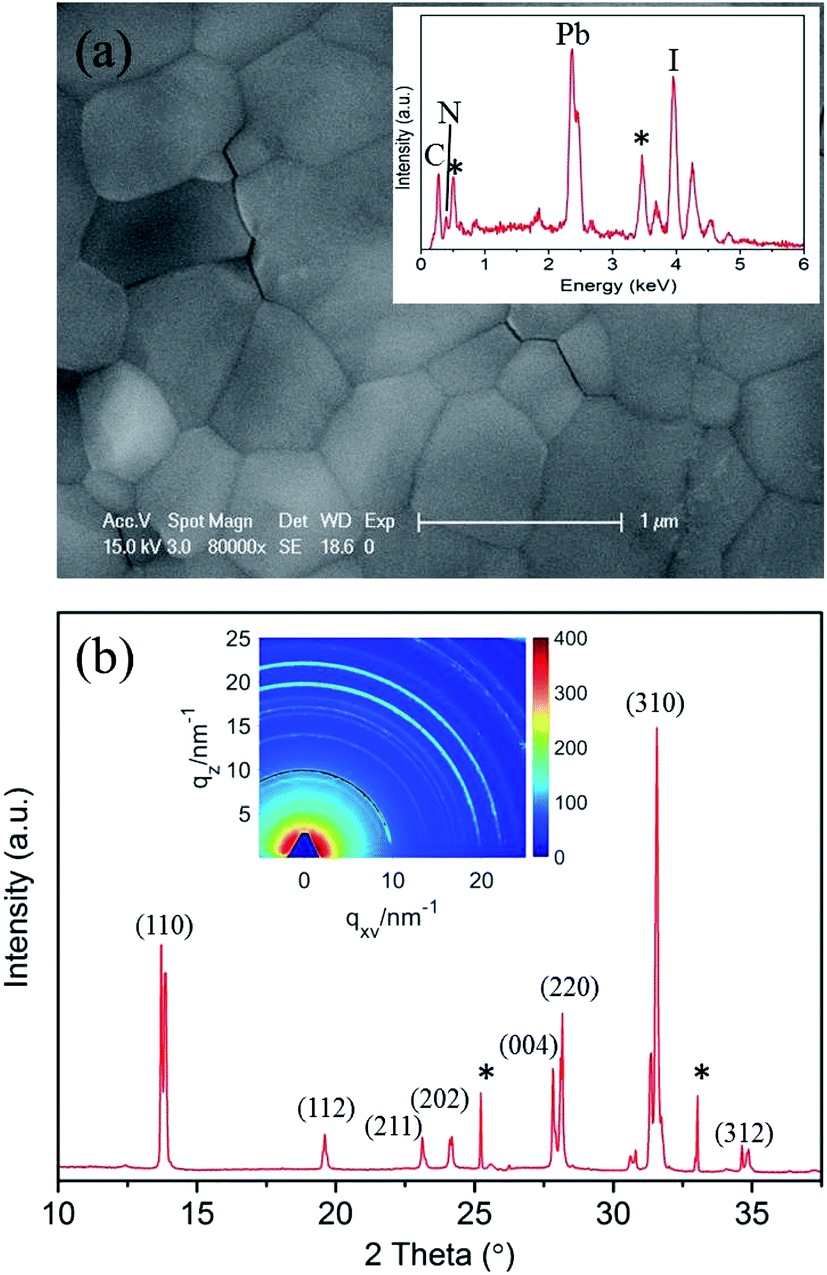 | ||
| Fig. 1 (a) SEM image of the as-prepared CH3NH3PbI3 film on FTO glass. The inset is the EDX spectrum of the CH3NH3PbI3 film. (b) XRD spectrum of the CH3NH3PbI3 film extracted from the 2D GIXRD pattern in the out-of-plane direction. The inset is the 2D GIXRD pattern in q-space taken with an incident X-ray angle of 0.2°. | ||
The corresponding X-ray diffraction (XRD) spectrum of the CH3NH3PbI3 film is shown in Fig. 1b. The spectrum was extracted from the 2D GIXRD pattern in q-space taken with an incident X-ray angle of 0.2° (the inset of Fig. 1b), and the peak positions match well with those of the reported tetragonal CH3NH3PbI3 perovskite structure and the calculated a = 8.855 Å and c = 12.659 Å.40,41
In optoelectronic device applications, CH3NH3PbI3 films are usually grown on a titanium dioxide frame. Therefore, to investigate the film structure evolution under the humid atmosphere by in situ GIXRD measurements, CH3NH3PbI3 films were prepared on conventional TiO2 nanoparticle films in the first step. The SEM images of the bare TiO2 nanoparticle film and following fabricated CH3NH3PbI3 films are shown in Fig. 2a and b, which confirm the uniformity of the prepared CH3NH3PbI3 films.
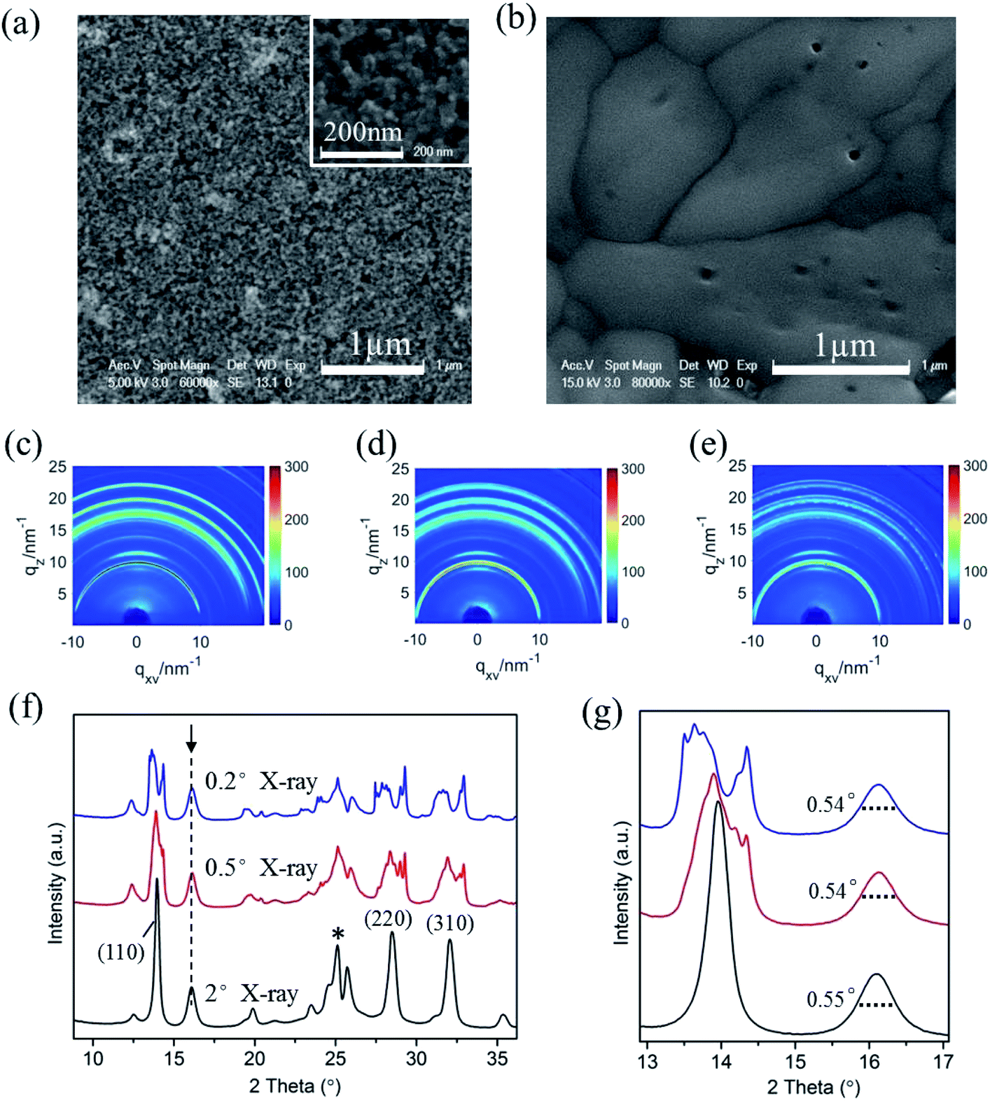 | ||
| Fig. 2 SEM images of (a) bare TiO2 nanoparticle film and (b) fabricated CH3NH3PbI3 films; the inset of (a) is a high magnification image of porous TiO2 nanoparticles. (c)–(e) The two-dimensional diffraction signals of the CH3NH3PbI3/TiO2 NP films exposed to 55% relative humidity using incident measurement grazing angles of 2°, 0.5°, and 0.2°. (f) The dimensional diffraction spectrum integrated from (c–e) in the out-of-plane direction. (g) The magnified XRD spectrum of (f) for obtaining the FWHM of the crystal planes. | ||
We used different incident X-ray grazing angles to study the evolution of the crystal structure from bulk to surface in moisture environment. Fig. 2c–e shows the in situ GIXRD pattern of the perovskite film in an environment of 50% relative humidity with grazing angles of 2°, 0.5° and 0.2°. The three main peaks at the diffraction vector q = 10, 20, 22.1 nm−1 correspond to the (110), (220), and (310) planes of the tetragonal perovskite crystal structure.42 Fig. 2f is the one-dimensional diffraction spectrum corresponding to Fig. 2c–e, obtained by azimuth integration in the out-of-plane direction. An additional peak at 16.1° (q = 11 nm−1) can be observed once the CH3NH3PbI3/TiO2 NPs are exposed to 50% relative humidity, irrespective of the X-ray incident angle. This peak indicates a new intermediate structure that is different from the reported PbI2 and CH3NH3I.43 The uniform diffraction ring with high intensity along the out-of-plane direction in Fig. 2c–e confirms that the intermediate has anisotropic planes parallel to the substrate.
CH3NH3PbI3 typically has a tetragonal perovskite structure (space group I4/mcm) at room temperature.37,44 The methyl ammonium CH3NH3+ cations are localized to the area between the two [PbI6]4− octahedral layers. The organic and inorganic components interact by hydrogen bonds between the amino group and the halide ions, whereas weak van der Waals interactions exist among the organic components. Depending on the occupation and orientation of the organic amino cations, the spacing between the inorganic layers is accordingly changeable. When the organometal halide perovskite CH3NH3PbI3 is exposed to a humid environment, the adsorbed water molecules on the perovskite surfaces rapidly extract protons from organic amino cations. Due to the soft nature of organic CH3NH3+ cations, intrinsic degradation occurs in perovskite materials upon the breaking of the bonds and with the generated excitation stresses, producing some 2D [PbI6]4− octahedral pieces from the partly cracked 3D [PbI6]4− octahedral network. The newly denoted XRD peak at 16.1° (q = 11 nm−1) matches the reported 2D [PbI6]4− octahedral crystals.45,46 This finding is basically in accordance with the report by Kelly et al. that the distortion of [PbI6]4− octahedrons leads to a multiphase structure in perovskite crystal degradation.37
In addition, it is observed that the (110), (220), and (310) planes are split obviously for the CH3NH3PbI3/TiO2 NPs when the X-ray incident grazing angle decreases from 2° to 0.2° (Fig. 2f) in 50% RH moisture. This is attributed to the large and wide distributed crystal grains of perovskite in the direction perpendicular to these diffraction surfaces. In general, sharp diffraction peaks originate from the large grains, which lead to discontinuous 2D diffraction rings and separated peaks at small grazing angles. Besides, the stress located at the large perovskite CH3NH3PbI3 crystal surfaces may also results in their planes split at low incident grazing angle, especially the prolonged spot size enlarged surface stress effect.
The crystallite sizes of the intermediate 2D [PbI6]4− intermediates can be obtained quantitatively from their respective enlarged XRD patterns (Fig. 2g) by using the Scherrer equation:47,48
Furthermore, the characteristic peak intensity of CH3NH3PbI3 is decreased in the small X-ray grazing angle (0.2°) GIXRD measurement, while the peaks of nondegraded perovskite samples are not changed obviously (ESI Fig. S3†). This result provides evidence that the CH3NH3PbI3 perovskite crystals are degraded from the surface to the bulk, which indicates that the induced lattice stress released privilege from the high-energy perovskite crystal surfaces.
As the relative humidity increases from 55% RH to 80% RH shown in Fig. 3a–c, the characteristic peak intensity of CH3NH3PbI3 is decreased, see the azimuth integration in the out-of-plane direction in Fig. 3d. With the rise of humidity, the peak intensity increase of 2D [PbI6]4− octahedral pieces is not obvious due to the first degradation stage complete at the surface range, although the perovskite degradation continues in bulk. Compared with the network coverage of the CH3NH3PbI3 film on TiO2 nanoparticles, the surface morphology deteriorates significantly after the in situ humidity experiment (Fig. 3e). The crystal grains were partly separated and the porosity between the grains increased obviously. This indicates that new grain boundaries are generated accompanied by the breakage of perovskite crystalline structures, which is in accordance with the GIXRD analysis of CH3NH3PbI3 degradation in moisture.
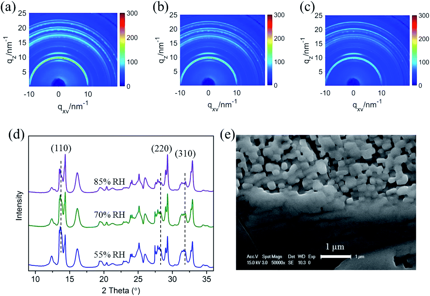 | ||
| Fig. 3 (a)–(c) The two-dimensional diffraction signals of the CH3NH3PbI3/TiO2 NP films exposed to 55%, 70%, and 85% relative humidity using an incident measurement grazing angle of 0.2°. (d) The one-dimensional diffraction spectrum integrated from (a–c) in the out-of-plane direction. (e) SEM image of CH3NH3PbI3/TiO2 NP film after the in situ crystal study in a moist environment. | ||
An XANES study was performed to further examine the degradation of CH3NH3PbI3 on TiO2 nanoparticle films in moisture. The XANES measurement was carried out by using the total electron yield (TEY) mode under high vacuum conditions of 8 × 10⁻⁶ torr. The photon flux of the incident beam (I0) was simultaneously obtained by monitoring the photocurrent of the Au grid which is located in front of the entrance of the terminal station. In Fig. 4a, the K-edge XANES of element nitrogen probes N 2p electronic states, and the main peak at ∼406 eV is attributed to the C–N σ* transitions. The peak intensity decreases obviously after the CH3NH3PbI3/TiO2 NP films are exposed to moisture. It indicated that partial hydrogen bonds between organic amino and halide ions, as well as weak van der Waals interactions between organic components, were altered. The protons of the CH3NH3+ cation are extracted by the adhesive water molecules and decomposed into volatile methylamine, thereby reducing C–N σ* transitions.
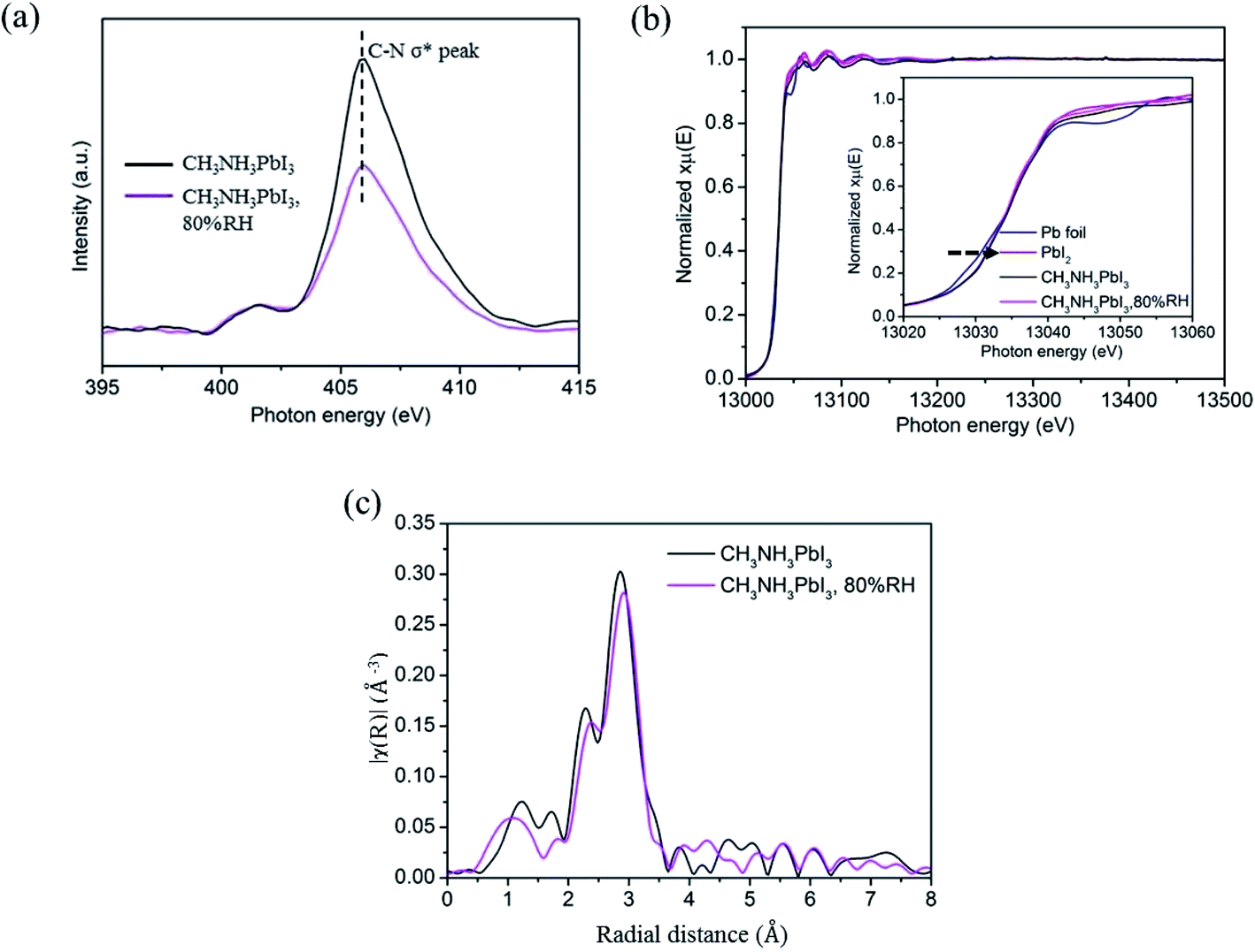 | ||
| Fig. 4 Schematic diagrams of XANES measurements of (a) nitrogen K-edge and (b) lead L-edge of CH3NH3PbI3 perovskite film before and after exposure to moisture. (c) EXAFS spectra in R-space of perovskite films before and after exposure to moisture with 80% relatively humidity. | ||
In order to further investigate the influence of moisture, XAFS based on synchrotron radiation was used to detect the electronic structure of perovskite. The local environment of Pb was examined by measuring Pb L3-edge (Pb 2p3/2 core electron to nd unoccupied states) via fluorescence detection mode. The X-ray absorption near edge structure (XANES) and extended X-ray absorption fine structure (EXAFS) spectra were analyzed by standard procedure with Athena software package49 There is an obvious linear relationship between the absorption edge and the valence state, and the transition to high energy indicates that there is a higher valence state in the sample. Pb is commonly presented as a divalent cation (s2p0), the XANES spectra of all the samples are close to the Pb2+ state except the Pb0 state of standard Pb foil, as shown in Fig. 4b. The results showed that the chemical state of Pb did not change significantly in the in situ wet experiment, which indicates that the [PbI6]4− octahedral crystals were not broken in the first stage of CH3NH3PbI3 degradation.
The tetragonal perovskite structure is not absolutely symmetrical, which means that the Pb–I bond length in the b-axis direction differs from that in the ac plane. The two peaks at 2–3 Å in R-space of EXAFS spectrum (Fig. 5c) could be specified as the two coordinating peaks of Pb–I, which are defined as Pb–I1 (R = 2.4 Å) and Pb–I2 (R = 2.8 Å).50 It can be observed that the two peaks move to large radial distance after exposure in 80% relative humidity, which suggests that the distance between the central Pb atom and the I atom is increased, that is, the Pb–I bond tends to unstable. The fitting results of Pb L3 EXAFS by scattering from a single coordination shell of iodine shown in Table S1† further prove the analyses. What's more, the Debye–Waller factor, namely the degree of disorder of CH3NH3PbI3 is significantly when it is exposed in 80% relative humidity, which provide evidence that the introduction of water will reduce crystal symmetry and increase the distortion of [PbI6]4− octahedral, thereby generating some two-dimensional network of [PbI6]4− octahedra intermediate and increasing the degree of disorder.
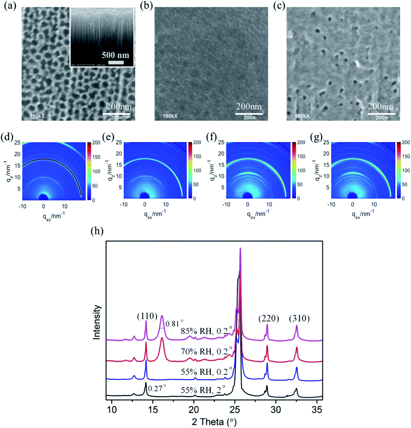 | ||
| Fig. 5 SEM images of (a) bare TiO2 nanotube films, (b) fabricated CH3NH3PbI3 films deposited on TiO2 nanotubes, and (c) degraded CH3NH3PbI3 films deposited on TiO2 nanotubes after the in situ humidity experiment. The inset of Fig. 2a is the cross-sectional SEM image of the vertical TiO2 nanotubes. (d and e) The 2D GIXRD patterns in q space of the CH3NH3PbI3/TiO2 films in the environment of 55% relative humidity, incident X-ray grazing angles of 2° and 0.2°, respectively. (f and g) The 2D GIXRD patterns of the CH3NH3PbI3/TiO2 films with relative humidity at 65% RH and 80% RH. (h) The exacted one-dimensional diffraction spectrum for Fig. 5d–g obtained by integrating the azimuth with the same q. | ||
The comprehensive results obtained by in situ GIXRD and XANES measurements performed at controlled relative humidity demonstrate that intermediate [PbI6]4− octahedral crystals are induced, which is strongly linked with the progress of chemical degradation in CH3NH3PbI3 perovskite films.
To confirm the intermediate crystal structure and evaluate the substrate effect on CH3NH3PbI3 stability in optoelectronics, crystalline anodic TiO2 nanotube arrays were introduced as substrates for perovskite CH3NH3PbI3 films. Highly ordered TiO2 nanotube arrays were fabricated on titanium foil by an electrochemical anodization method that we reported elsewhere.51–53 The morphologies of the bare TiO2 nanotubes with uniform regular pores can be observed in Fig. 5a, and the inset SEM image of the cross-sectional morphology confirms its vertical tubular structure. The tube arrays formed on the Ti foil are 2 μm in length and 60 nm in diameter, with a pore size of ∼50 nm. CH3NH3PbI3 perovskite film was prepared on TiO2 NT arrays by a sequential deposition method, which is described in the experiment section. The TiO2 nanotube arrays were perfectly covered by the CH3NH3PbI3 perovskite films with good uniformity, as shown in Fig. 5b.
Next, in situ GIXRD measurements were taken for the CH3NH3PbI3/TiO2 NTs to study their degradation in a moist environment. The 2D GIXRD pattern of such perovskite films under the environment of 50% RH is shown in Fig. 5d and e, with incident X-ray grazing angles of 2° and 0.2°, while Fig. 5f and g demonstrates their GIXRD patterns with higher relative humidity at 65% RH and 80% RH. The exacted one-dimensional diffraction spectrum for Fig. 5d–g is shown in Fig. 5h by integrating the azimuth with the same q. The three main crystal planes of (110), (220), and (310) for the tetragonal perovskite structure at the diffraction vectors q = 10, 20, and 22.1 nm−1 are the same as those of the CH3NH3PbI3/TiO2 NPs for all spectra. However, no split is observed for these crystal planes even at small grazing angles, which indicates that the crystal size of the CH3NH3PbI3 perovskite on the TiO2 nanotubes is uniform and smaller than that of the TiO2 nanoparticle films. The regular pores of the nanotubes likely confine the crystal growth and formation of the CH3NH3PbI3 perovskite.
No intermediate phase (2theta = 16°) is observed when the CH3NH3PbI3/TiO2 NTs are exposed to 50% RH moisture at both 2° and 0.2° grazing angles, which is different from the demonstrated CH3NH3PbI3/TiO2 NPs (Fig. 3d). When the controlled humidity is increased up to 65% RH, the same intermediate phase with an FWHM of 0.81° at q = 11 nm−1 (2theta = 16°) is observed. The crystallite sizes of the intermediate [PbI6]4− octahedral crystals are calculated to be 7.9 nm by using the Scherrer equation, which is much smaller than that of the intermediate crystals in the degraded CH3NH3PbI3/TiO2 NPs. When the CH3NH3PbI3 perovskite is infiltrated into the surface of TiO2 nanotube arrays, the regular pores of such crystalline nanotubes probably confine the 3D [PbI6]4− octahedral crystal network and restrain the intermediate formation induced by the broken bonds from organic amino cations. Thus, the degradation of the CH3NH3PbI3 perovskite using the TiO2 nanotube substrate is relatively slow compared with that of the conventional TiO2 nanoparticles in moisture.
The surface morphology of the CH3NH3PbI3/TiO2 NTs is shown in Fig. 5c after the in situ humidity experiment. Sporadic pores are observed compared with the uniform coverage of the CH3NH3PbI3 film (Fig. 5b). No cracks or new grain boundaries are found, which indicates that the deformation of perovskite crystals is restrained by the bottom TiO2 nanotube arrays, slowing the degradation of the CH3NH3PbI3/TiO2 NTs in a moist environment. The SEM observations are in accordance with the GIXRD analysis of the CH3NH3PbI3/TiO2 NT degradation in moisture.
To evaluate the X-ray scintillation properties of the organometal halide perovskite film after incorporating the anodic TiO2 nanotube substrate, we measured the light output by XEOL for the as-prepared CH3NH3PbI3 films deposited on both TiO2 NP and TiO2 NT substrates with excitation at 40 keV. Fig. S4† shows the measurement setup for the XEOL emission spectrum. In this setup, a monochromatic X-ray beam illuminated the CH3NH3PbI3/TiO2 NTs at normal incidence, and the fluorescence emitted through the film was collected by an optical fiber and transferred to a grating spectrometer. The measured emission spectra of the CH3NH3PbI3/TiO2 NPs and CH3NH3PbI3/TiO2 NTs are shown in Fig. 6a. Both perovskite films demonstrate a single XEOL peak centered at 790 nm, which matches the band gaps (1.57 eV) of reported tetragonal CH3NH3PbI3 perovskites.3,54,55
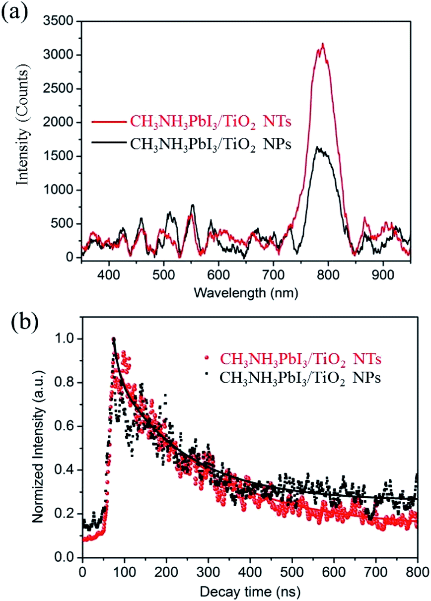 | ||
| Fig. 6 (a) XEOL spectra of CH3NH3PbI3/TiO2 NPs and CH3NH3PbI3/TiO2 NTs with 40 keV X-ray excitation. (b) The experimental data of the fluorescence decay curve at 790 nm excited with a 40 keV excitation, and the solid lines are fitting curves. | ||
The full width half maximums (FWHMs) of the XEOL peak are 57 nm and 53 nm for the CH3NH3PbI3/TiO2 NPs and CH3NH3PbI3/TiO2 NTs, respectively. The broad XEOL spectra are attributed to the high photon energy of the X-rays, in which the electrons are excited to high energy levels in the conduction band, resulting in a broad emission when the excited electrons relax to different lower energy levels. The enhancement of visible light output is observed between 750 nm and 850 nm for the CH3NH3PbI3 perovskite fabricated on TiO2 nanotube arrays. The XEOL peak intensity of the CH3NH3PbI3/TiO2 NTs is enhanced by 88% compared with that of the TiO2 nanoparticle films at 790 nm. Small organometal halide perovskites have a larger exciton binding energy than large crystals.56 Herein, the small crystal size of the CH3NH3PbI3 perovskite confined by TiO2 nanotubes contributes to the relatively high exciton binding energy, increasing exciton recombination and light output efficiency. In addition, the improved stability and crystallinity of the CH3NH3PbI3 crystals fabricated on TiO2 nanotubes contributes to its improved emission intensity.
The decay of fluorescence excited by the X-ray was measured using a Time-Correlated Single Photon Counting (TCSPC) method. Fluorescence decay profile can be fitted by a two exponential function, I(t) = A0 + A1 × exp(−t/τ1) + A2 × exp(−t/τ2), where τ1 and τ2 denote the decay times for the faster and the slower component, respectively, and A1 and A2 are the amplitudes, as presented in Table S2.† The dominant faster lifetimes τ1 for CH3NH3PbI3 prepared on both TiO2 nanotubes and TiO2 nanoparticles films at 790 nm are all about 12 ns, while the slower lifetimes τ2 are 220 and 170 ns at 790 nm, as shown in Fig. 5b. The faster and slower decay represent the non-radiative recombination and free exciton recombination, respectively. The lifetime for the CH3NH3PbI3 prepared on both TiO2 nanotubes are longer than that deposited on TiO2 nanoparticles, which demonstrates the perovskite CH3NH3PbI3 prepared on TiO2 nanotubes has good crystallinity and scintillation property with less crystal distortion.
Except for the CH3NH3PbI3 perovskite, the method of incorporating TiO2 nanotubes as a substrate is demonstrated to increase the scintillation properties in other systems. The light output for the CH3NH3PbBr3 perovskite prepared on TiO2 nanotubes is 75% higher than that on the TiO2 nanoparticle substrate, which has the same tendency as CH3NH3PbI3, see ESI Fig. S5.† Incorporating TiO2 nanotubes is likely a universal method to increase XEOL intensity and scintillation applications.
4. Conclusion
We used in situ high-resolution 2D GIXRD to determine the structural evolution of perovskite CH3NH3PbI3 prepared on both conventional porous TiO2 nanoparticles and anodic TiO2 nanotubes in controlled relative humidity. The GIXRD and XANES measurements suggest that some 2D network of [PbI6]4− octahedra is constructed for the intermediate structure. We also show that the intermediate is observed once the CH3NH3PbI3/TiO2 NPs are exposed to humidity 50% RH, while the same intermediate appears at 65% RH for CH3NH3PbI3/TiO2 NTs. The regular pores of TiO2 nanotube arrays confine the 3D [PbI6]4− octahedral network, reducing ion migration and octahedral agglomeration and improving the stability and crystallinity of the assisted organometal halide CH3NH3PbI3 perovskite. Compared with the conventional TiO2 nanoparticle substrate, the XEOL peak intensity of CH3NH3PbI3 is increased up to 88% by incorporating anodic TiO2 NTs. These results help elucidate fundamental decomposition pathways in organolead halide perovskite films and contribute paths for further scintillation applications in perovskites.Conflicts of interest
We declare that we have no conflict of interest.Acknowledgements
We acknowledge financial support from the National Science Foundation of China (12004070, U2032128, 11505280), the Shanghai Natural Science Foundation and Sailing Program (19ZR1463300, 17YF1400600). The authors thank the support from staff in beamline BL08U1A, BL14B, BL13W and BL14W in Shanghai Synchrotron Radiation Facility (SSRF) for sample characterization.References
- P. Qin, S. Tanaka, S. Ito, N. Tetreault, K. Manabe, H. Nishino, M. K. Nazeeruddin and M. Grätzel, Nat. Commun., 2014, 5, 3834 CrossRef CAS.
- H. Min, M. Kim, S.-U. Lee, H. Kim, G. Kim, K. Choi, J. H. Lee and S. I. Seok, Science, 2019, 366, 749–753 CrossRef CAS.
- H.-S. Kim, C.-R. Lee, J.-H. Im, K.-B. Lee, T. Moehl, A. Marchioro, S.-J. Moon, R. Humphry-Baker, J.-H. Yum, J. E. Moser, M. Grätzel and N.-G. Park, Sci. Rep., 2012, 2, 591 CrossRef.
- G. Xing, N. Mathews, S. Sun, S. S. Lim, Y. M. Lam, M. Grätzel, S. Mhaisalkar and T. C. Sum, Science, 2013, 342, 344–347 CrossRef CAS.
- D. Gedamu, I. M. Asuo, D. Benetti, M. Basti, I. Ka, S. G. Cloutier, F. Rosei and R. Nechache, Sci. Rep., 2018, 8, 12885 CrossRef.
- X. Li, D. Bi, C. Yi, J.-D. Décoppet, J. Luo, S. M. Zakeeruddin, A. Hagfeldt and M. Grätzel, Science, 2016, 353, 58–62 CrossRef CAS.
- C. S. Ponseca, T. J. Savenije, M. Abdellah, K. Zheng, A. Yartsev, T. Pascher, T. Harlang, P. Chabera, T. Pullerits, A. Stepanov, J.-P. Wolf and V. Sundström, J. Am. Chem. Soc., 2014, 136, 5189–5192 CrossRef CAS.
- H. Zhou, Q. Chen, G. Li, S. Luo, T.-B. Song, H.-S. Duan, Z. Hong, J. You, Y. Liu and Y. Yang, Science, 2014, 345, 542–546 CrossRef CAS.
- W. Chen, Y. Wu, Y. Yue, J. Liu, W. Zhang, X. Yang, H. Chen, E. Bi, I. Ashraful, M. Grätzel and L. Han, Science, 2015, 350, 944–948 CrossRef CAS.
- W. S. Yang, B.-W. Park, E. H. Jung, N. J. Jeon, Y. C. Kim, D. U. Lee, S. S. Shin, J. Seo, E. K. Kim, J. H. Noh and S. I. Seok, Science, 2017, 356, 1376–1379 CrossRef CAS.
- F. Sahli, J. Werner, B. A. Kamino, M. Bräuninger, R. Monnard, B. Paviet-Salomon, L. Barraud, L. Ding, J. J. Diaz Leon, D. Sacchetto, G. Cattaneo, M. Despeisse, M. Boccard, S. Nicolay, Q. Jeangros, B. Niesen and C. Ballif, Nat. Mater., 2018, 17, 820–826 CrossRef CAS.
- L. Wang, H. Zhou, J. Hu, B. Huang, M. Sun, B. Dong, G. Zheng, Y. Huang, Y. Chen, L. Li, Z. Xu, N. Li, Z. Liu, Q. Chen, L.-D. Sun and C.-H. Yan, Science, 2019, 363, 265–270 CrossRef CAS.
- E. H. Jung, N. J. Jeon, E. Y. Park, C. S. Moon, T. J. Shin, T.-Y. Yang, J. H. Noh and J. Seo, Nature, 2019, 567, 511–515 CrossRef CAS.
- H. Lu, Y. Liu, P. Ahlawat, A. Mishra, W. R. Tress, F. T. Eickemeyer, Y. Yang, F. Fu, Z. Wang, C. E. Avalos, B. I. Carlsen, A. Agarwalla, X. Zhang, X. Li, Y. Zhan, S. M. Zakeeruddin, L. Emsley, U. Rothlisberger, L. Zheng, A. Hagfeldt and M. Grätzel, Science, 2020, 370, eabb8985 CrossRef CAS.
- B. Zhao, S. Bai, V. Kim, R. Lamboll, R. Shivanna, F. Auras, J. M. Richter, L. Yang, L. Dai, M. Alsari, X.-J. She, L. Liang, J. Zhang, S. Lilliu, P. Gao, H. J. Snaith, J. Wang, N. C. Greenham, R. H. Friend and D. Di, Nat. Photonics, 2018, 12, 783–789 CrossRef CAS.
- Z.-K. Tan, R. S. Moghaddam, M. L. Lai, P. Docampo, R. Higler, F. Deschler, M. Price, A. Sadhanala, L. M. Pazos, D. Credgington, F. Hanusch, T. Bein, H. J. Snaith and R. H. Friend, Nat. Nanotechnol., 2014, 9, 687–692 CrossRef CAS.
- J. Xing, F. Yan, Y. Zhao, S. Chen, H. Yu, Q. Zhang, R. Zeng, H. V. Demir, X. Sun, A. Huan and Q. Xiong, ACS Nano, 2016, 10, 6623–6630 CrossRef CAS.
- X. Y. Chin, D. Cortecchia, J. Yin, A. Bruno and C. Soci, Nat. Commun., 2015, 6, 7383 CrossRef CAS.
- A. Perumal, S. Shendre, M. Li, Y. K. E. Tay, V. K. Sharma, S. Chen, Z. Wei, Q. Liu, Y. Gao, P. J. S. Buenconsejo, S. T. Tan, C. L. Gan, Q. Xiong, T. C. Sum and H. V. Demir, Sci. Rep., 2016, 6, 36733 CrossRef CAS.
- A. B. Wong, M. Lai, S. W. Eaton, Y. Yu, E. Lin, L. Dou, A. Fu and P. Yang, Nano Lett., 2015, 15, 5519–5524 CrossRef CAS.
- A. L. Palma, L. Cinà, Y. Busby, A. Marsella, A. Agresti, S. Pescetelli, J.-J. Pireaux and A. Di Carlo, ACS Appl. Mater. Interfaces, 2016, 8, 26989–26997 CrossRef CAS.
- C. Huang, C. Zhang, S. Xiao, Y. Wang, Y. Fan, Y. Liu, N. Zhang, G. Qu, H. Ji, J. Han, L. Ge, Y. Kivshar and Q. Song, Science, 2020, 367(6481), 1018–1021 CrossRef CAS.
- C. Qin, A. S. D. Sandanayaka, C. Zhao, T. Matsushima, D. Zhang, T. Fujihara and C. Adachi, Nature, 2020, 585, 53–57 CrossRef CAS.
- S. Yakunin, M. Sytnyk, D. Kriegner, S. Shrestha, M. Richter, G. J. Matt, H. Azimi, C. J. Brabec, J. Stangl, M. V. Kovalenko and W. Heiss, Nat. Photonics, 2015, 9, 444–449 CrossRef CAS.
- S. Shrestha, R. Fischer, G. J. Matt, P. Feldner, T. Michel, A. Osvet, I. Levchuk, B. Merle, S. Golkar, H. Chen, S. F. Tedde, O. Schmidt, R. Hock, M. Rührig, M. Göken, W. Heiss, G. Anton and C. J. Brabec, Nat. Photonics, 2017, 11, 436–440 CrossRef CAS.
- Y. C. Kim, K. H. Kim, D.-Y. Son, D.-N. Jeong, J.-Y. Seo, Y. S. Choi, I. T. Han, S. Y. Lee and N.-G. Park, Nature, 2017, 550, 87–91 CrossRef CAS.
- J. A. Steele, W. Pan, C. Martin, M. Keshavarz, E. Debroye, H. Yuan, S. Banerjee, E. Fron, D. Jonckheere, C. W. Kim, W. Baekelant, G. Niu, J. Tang, J. Vanacken, M. Van Der Auweraer, J. Hofkens and M. B. J. Roeffaers, Adv. Mater., 2018, 30, 1804450 CrossRef.
- F. Ye, H. Lin, H. Wu, L. Zhu, Z. Huang, D. Ouyang, G. Niu and W. C. H. Choy, Adv. Funct. Mater., 2019, 29, 1806984 CrossRef.
- B. Náfrádi, G. Náfrádi, L. Forró and E. Horváth, J. Phys. Chem. C, 2015, 119, 25204–25208 CrossRef.
- Y. Zhang, R. Sun, X. Ou, K. Fu, Q. Chen, Y. Ding, L.-J. Xu, L. Liu, Y. Han, A. V. Malko, X. Liu, H. Yang, O. M. Bakr, H. Liu and O. F. Mohammed, ACS Nano, 2019, 13, 2520–2525 CrossRef CAS.
- G. Grancini, C. Roldán-Carmona, I. Zimmermann, E. Mosconi, X. Lee, D. Martineau, S. Narbey, F. Oswald, F. De Angelis, M. Graetzel and M. K. Nazeeruddin, Nat. Commun., 2017, 8, 15684 CrossRef CAS.
- J.-P. Correa-Baena, M. Saliba, T. Buonassisi, M. Grätzel, A. Abate, W. Tress and A. Hagfeldt, Science, 2017, 358, 739–744 CrossRef CAS.
- J. A. Christians, P. A. Miranda Herrera and P. V. Kamat, J. Am. Chem. Soc., 2015, 137, 1530–1538 CrossRef CAS.
- J. H. Noh, S. H. Im, J. H. Heo, T. N. Mandal and S. I. Seok, Nano Lett., 2013, 13, 1764–1769 CrossRef CAS.
- Y. Tian, C. Zhou, M. Worku, X. Wang, Y. Ling, H. Gao, Y. Zhou, Y. Miao, J. Guan and B. Ma, Adv. Mater., 2018, 30, 1707093 CrossRef.
- G. Niu, X. Guo and L. Wang, J. Mater. Chem. A, 2015, 3, 8970–8980 RSC.
- J. Yang, B. D. Siempelkamp, D. Liu and T. L. Kelly, ACS Nano, 2015, 9, 1955–1963 CrossRef CAS.
- Q. Hu, L. Zhao, J. Wu, K. Gao, D. Luo, Y. Jiang, Z. Zhang, C. Zhu, E. Schaible, A. Hexemer, C. Wang, Y. Liu, W. Zhang, M. Grätzel, F. Liu, T. P. Russell, R. Zhu and Q. Gong, Nat. Commun., 2017, 8, 15688 CrossRef CAS.
- J. M. Frost, K. T. Butler, F. Brivio, C. H. Hendon, M. Van Schilfgaarde and A. Walsh, Nano Lett., 2014, 14, 2584–2590 CrossRef CAS.
- L. Etgar, P. Gao, Z. Xue, Q. Peng, A. K. Chandiran, B. Liu, M. K. Nazeeruddin and M. Grätzel, J. Am. Chem. Soc., 2012, 134, 17396–17399 CrossRef CAS.
- T. Baikie, Y. Fang, J. M. Kadro, M. Schreyer, F. Wei, S. G. Mhaisalkar, M. Graetzel and T. J. White, J. Mater. Chem. A, 2013, 1, 5628–5641 RSC.
- Z.-K. Wang, M. Li, Y.-G. Yang, Y. Hu, H. Ma, X.-Y. Gao and L.-S. Liao, Adv. Mater., 2016, 28, 6695–6703 CrossRef CAS.
- S. Maryam, R. Saidah, N. Mufti, S. Sunaryono and A. Fuad, Mater. Today: Proc., 2019, 13, 205–210 CAS.
- Y. Kawamura, H. Mashiyama and K. Hasebe, J. Phys. Soc. Jpn., 2002, 71, 1694–1697 CrossRef CAS.
- W. Peng, J. Yin, K.-T. Ho, O. Ouellette, M. De Bastiani, B. Murali, O. El Tall, C. Shen, X. Miao, J. Pan, E. Alarousu, J.-H. He, B. S. Ooi, O. F. Mohammed, E. Sargent and O. M. Bakr, Nano Lett., 2017, 17, 4759–4767 CrossRef CAS.
- M. Hirasawa, T. Ishihara and T. Goto, J. Phys. Soc. Jpn., 1994, 63, 3870–3879 CrossRef CAS.
- S. Ghodke, S. Sonawane, R. Gaikawad and K. C. Mohite, Can. J. Chem. Eng., 2012, 90, 1153–1159 CrossRef CAS.
- I. Hernández, A. Maubert, L. Rendon Vazquez, P. Santiago, H. Hernández, L. Arceo, V. Febles, E. P. González and L. González-Reyes, Int. J. Electrochem. Sci., 2012, 7, 8832–8847 Search PubMed.
- B. Liu, R. Cui, H. Huang, X. Guo, S. Zuo, J. Dong, H. Yao, Y. Li, D. Zhao, J. Wang, J. Zhang, Y. Chen, J. Yang and B. Sun, Sol. Energy, 2020, 205, 202–210 CrossRef CAS.
- B. Gilbert, B. H. Frazer, A. Belz, P. G. Conrad, K. H. Nealson, D. Haskel, J. C. Lang, G. Srajer and G. De Stasio, J. Phys. Chem. A, 2003, 107, 2839–2847 CrossRef CAS.
- H. Li, Z. Chen, C. K. Tsang, Z. Li, X. Ran, C. Lee, B. Nie, L. Zheng, T. Hung, J. Lu, B. Pan and Y. Y. Li, J. Mater. Chem. A, 2014, 2, 229–236 RSC.
- H. Li, J. Zhang, J.-W. Cheng, Z. Chen, F. Liang, C.-K. Tsang, H. Cheng, L. Zheng, S.-T. Lee and Y. Li, ECS J. Solid State Sci. Technol., 2012, 1, M6–M9 CrossRef CAS.
- H. Li, J.-W. Cheng, S. Shu, J. Zhang, L. Zheng, C. K. Tsang, H. Cheng, F. Liang, S.-T. Lee and Y. Y. Li, Small, 2013, 9, 37–44 CrossRef CAS.
- M. M. Lee, J. Teuscher, T. Miyasaka, T. N. Murakami and H. J. Snaith, Science, 2012, 338, 643–647 CrossRef CAS.
- A. Kojima, K. Teshima, Y. Shirai and T. Miyasaka, J. Am. Chem. Soc., 2009, 131, 6050–6051 CrossRef CAS.
- S. Kumar, J. Jagielski, S. Yakunin, P. Rice, Y.-C. Chiu, M. Wang, G. Nedelcu, Y. Kim, S. Lin, E. J. G. Santos, M. V. Kovalenko and C.-J. Shih, ACS Nano, 2016, 10, 9720–9729 CrossRef CAS.
Footnote |
| † Electronic supplementary information (ESI) available. See DOI: 10.1039/d0ra08881a |
| This journal is © The Royal Society of Chemistry 2020 |