DOI:
10.1039/D0RA08746G
(Paper)
RSC Adv., 2020,
10, 45042-45058
Improved photoelectrode performance of chemical solution-derived Bi2O3 crystals via manipulation of crystal characterization
Received
14th October 2020
, Accepted 7th December 2020
First published on 21st December 2020
Abstract
Three-dimensional Bi2O3 crystals with various morphologies were successfully synthesized on F-doped tin oxide substrates with and without homoseed layers via chemical bath deposition (CBD) routes. The structural analysis reveals that control of the pH value of the reaction solution resulted in as-grown Bi2O3 crystals with nanosheet and plate morphologies. A lower pH value of the reaction solution engendered formation of a porous sheet-like morphology of Bi2O3; by contrast, a higher pH value of the reaction solution is favorable for formation of solid Bi2O3 plates on the substrates. Furthermore, a sputter coated Bi2O3 seed layer with dual α- and β-Bi2O3 phases plays an important role in the CBD-derived Bi2O3 crystallographic structures. The Bi2O3 crystals formed via CBD processes without a sputter coated Bi2O3 homoseed layer demonstrated a high purity in β-Bi2O3 phase; those grown with a homoseed layer exhibited a dual α/β phase. The photoactive performance results show that construction of an α/β-Bi2O3 homojunction in the CBD-derived Bi2O3 crystals substantially improved their photoactive performance. Comparatively, the porous Bi2O3 nanosheets with a dual α/β-Bi2O3 phase demonstrated the highest photoactive performance among various Bi2O3 crystals in this study. The superior photoactivity of the porous α/β-Bi2O3 nanosheets herein is attributed to their high light absorption capacity and photoinduced charge separation efficiency. The experimental results in this study provide a promising approach to design CBD-derived Bi2O3 crystals with desirable photoelectric conversion functions via facile morphology control and seed layer crystal engineering.
Introduction
Bi2O3 is an environmental friendly material, and it has received much attention due to its unique electrical and optical properties, which leads to its extensive usage in various scientific devices.1–3 Furthermore, it is a promising visible-light-driven photocatalyst with a narrow band gap (2.0–2.9 eV), and the valence band of bismuth oxide is made of a hybrid Bi 6s and O 2p orbit that decreases the symmetry of the band structure and leads to the corresponding dipoles which could enhance its photoactivity.4 Bi2O3 has different polymorphs;5 the monoclinic α and tetragonal β phases have been reported to exhibit superior photoactivity among various polymorphs.2,6 Recently, several works on synthesis of α-Bi2O3 crystals have been reported.7,8 By contrast, a relatively few works on synthesis of β-Bi2O3 crystals are proposed due to the difficulty of synthesizing the metastable β-phase.9 The β-Bi2O3 has a higher photoactivity than α-Bi2O3 because of its lower band gap energy and higher optical absorption in visible light region.10 Since the β-Bi2O3 phase represents a metastable high temperature modification and is known to transform readily to α-Bi2O3, controllable synthesis of defined β and α polymorphs and their stabilization at room temperature are complicated. Thus, the selective fabrication of β-Bi2O3 in a phase-pure form is still of great significance.
Bi2O3 crystals with various micro- and nanostructures, including nanosheet, nanorod, nanofiber, and sphere have been successfully synthesized via various chemical solution routes.11–14 Among various morphologies, nanosheet semiconductor oxides have drawn substantial research interest due to their unique geometry with outstanding electronic properties and high specific surface area, which could provide large amount of reaction sites and enable rapid charges generation and transport.15,16 Till now, various synthetic methods have been explored to prepare sheet- or plate-like β-Bi2O3 crystals with various surface features.11,17 All the above sheet- or plate-like Bi2O3 products exhibited outstanding visible-light-driven light harvesting ability and photoactive performance. For practical scientific applications, the cost of energy, time and raw materials required for synthesizing Bi2O3 crystals processes should be considered. Therefore, the chemical bath deposition (CBD) because of its large area deposition ability, low cost process, and easy process parameter control, is a promising route to be used for developing Bi2O3 crystal growth.18 Notably, several works have confirmed the importance of homoseed layer for the crystal growth behavior of various chemical route derived oxide crystals. For example, hydrothermal grown c-axis oriented zinc oxide nanorods were prepared on the c-axis oriented ZnO homoseed layer.19 The WO3 homoseed layer with desirable surface grain size shows important influence on the vertical alignment and aggregation in chemical route-derived one-dimensional WO3 crystals.20 Furthermore, homoseed layer of CuO has an important influence on the crystallinity and morphology of CuO crystals grown via CBD routes.21 In addition to the crystal growth behavior affected by the seed layer, the seed layer also dominates the as-grown crystals' characterization. However, systematical investigations of homoseed layer effect on CBD deposition of sheet- or plate-like Bi2O3 crystals and their resultant photoactive performance are not well proposed. In this study, a Bi2O3 homoseed layer was formed via sputtering deposition on substrates before the CBD Bi2O3 crystal growth. The present study introduces an important scientific aspect: the usage of a homoseed layer to improve the CBD process to change the growth and characteristics of two types of 3D Bi2O3 crystals has not been proposed so far. The effects of pre-formed Bi2O3 seed layer microstructures on the crystal features of the CBD-derived Bi2O3 crystals are demonstrated herein. Furthermore, the resultant crystal feature-dependent photoactive performance of various 3D Bi2O3 crystals with and without a homoseed layer is also discussed. The results herein are a good reference for design of chemical solution derived 3D Bi2O3 crystals with desirable photoactive performance with a homoseed layer engineering.
Experiments
Sample preparation
Various Bi2O3 crystals were synthesized by chemical bath deposition (CBD). Fluorine-tin-oxide (FTO) glass substrates were ultrasonically cleaned sequentially in distilled water, acetone and isopropyl alcohol. For preparation of CBD reaction solution, the 0.1 M bismuth nitrate was dissolved in deionized water to make 50 mL stock solution. A highly alkaline reaction solution was prepared by further adding 3 mL triethanolamine (TEA) as a complexing agent and 0.2 M NaOH. The FTO substrates were immersed vertically in a 200 mL beaker and the pH value of the resulting solution was adjusted to 10 and 13 with various addition contents of 0.1 M NaOH, and the subsequent CBD reaction of Bi2O3 crystals was carried out at 65 °C for 2 hours. The as-deposited samples were further annealed at 300 °C for 1 hour in ambient air to obtain crystalline Bi2O3 phase. For the preparation of seed layered CBD samples, the Bi2O3 homoseed layer was formed on the FTO substrates through post-annealing the sputtering deposited metallic Bi thin films at 400 °C in ambient air for 1 hour. The Bi metallic thin films were sputter deposited at room temperature with a pure Ar atmosphere. The working pressure during Bi thin-film growth was maintained at 2 Pa, and the sputtering power of the bismuth metallic target was fixed at 30 W. The distance between the FTO glass substrate and target is approximately 7 cm. Then the Bi2O3 seed layer coated FTO substrates were used to prepare the Bi2O3 crystals via CBD with the pH values of 10 and 13 as mentioned before. The sample codes of 10-Bi2O3, 13-Bi2O3, 10S-Bi2O3 and 13S-Bi2O3 represented Bi2O3 crystals formed at pH = 10 without a seed layer, pH = 13 without a seed layer, pH = 10 with a seed layer, and pH = 13 with a seed layer, respectively in this study.
The CBD route-derived Bi2O3 crystals herein are based on the following reaction steps:
In the nucleation process, bismuth nitrate reacts with the complexing (TEA) reagent by dissociating the bismuth ions as:
| | |
Bi(NO3)3 + N(CH2–CH2–OH)3 ⇆ [BiN(CH2–CH2–OH)3]3+ + 3NO3
| (1) |
| | |
[BiN(CH2–CH2–OH)3]3+ ⇆ Bi3+ + N(CH2–CH2–OH)3
| (2) |
The pH value of the solution was adjusted to 10 or 13 with NaOH solution herein to form Bi(OH)3:
| | |
Bi3+ + 3OH− ⇆ Bi(OH)3
| (4) |
After annealing in ambient air at the elevated temperature, the Bi(OH)3 converts into bismuth oxide (Bi2O3) via the following reaction.
| | |
2Bi(OH)3 ⇆ Bi2O3 + 3H2O
| (5) |
The thermal annealing treatment of the as-deposited film will cause oxygen to remove hydroxide ions and form the crystalline Bi2O3 crystals22
Materials analysis
Sample crystal structures were investigated by X-ray diffraction (XRD; Bruker D2 PHASER) analysis using Cu Kα radiation (wavelength: 0.15406 nm) with a two theta scan range of 20–60° and scan rate of four degrees per min. The surface morphology of the thin film sample was characterized by scanning electron microscope at an accelerating voltage of 15 kV (SEM; Hitachi S-4800). A transmission electron microscope was used to study the detailed microstructure of the Bi2O3 sample at 200 KV (HRTEM; Philips Tecnai F20 G2). To prepare the TEM test piece, first scrape off the nanostructures grown on the substrate into the absolute alcohol solution, and then drip a few drops from the solution into the copper mesh. Finally place it in a 90 °C oven for more than 12 hours. The diffuse reflectance spectra of the Bi2O3 samples were recorded by using UV-vis spectrophotometer (Jasco V750) with a scanning speed of 17 nm s−1 at the 300–700 nm range. The elemental binding states of the Bi2O3 crystals were explored by X-ray photoelectron spectroscopy (XPS ULVAC-PHI, PHI 5000 VersaProbe) using Mg Kα radiation. The electrochemical and photoelectrochemical properties of the samples were conducted by the potentiostat (SP150, BioLogic). The illumination excited from the 100 W Xe lamp combined with a 420 nm cut-off filter was used as the light source during the experiments. The Bi2O3 film grown on the 1 cm × 1 cm FTO glass was used as working electrode. Platinum and Ag/AgCl were used as counter and reference electrode respectively. The 0.5 M solution of Na2SO4 was used as electrolyte. The PEC measurement is carried out in a voltage of 1 V, and every 20 seconds is used as an interval for switching the lights. Electrochemical impedance spectroscopy (EIS) measurements were performed using the aforementioned potentiostat and the same electrode configuration. Furthermore, the Nyquist plots of various samples were measured at the open circuit potential with the frequency from 0.1 Hz to 150 kHz.
Results and discussion
Fig. 1(a)–(d) show the XRD patterns of various Bi2O3 films. In addition to the Bragg reflections originated from the FTO substrate, Fig. 1(a) and (b) show Bragg reflections centered at approximately, 27.95°, 31.76°, 32.69°, 46.22°, 46.91°, 54.27°, 55.63° and 57.76° corresponding to the (210), (002), (220), (222), (400), (203), (213) and (402) of the tetragonal structured β-Bi2O3 (β-Bi2O3: JCPDS no. 027-0050). No other crystalline phases were detected, confirming the phase purity of the β-Bi2O3 product for the 10-Bi2O3 and 13-Bi2O3 films. Furthermore, a substantially high intensity of the (201) Bragg reflection appeared in Fig. 1(a) and (b), revealing a preferred (201)-oriented β-Bi2O3 crystals dominated the crystallographic feature of the CBD-derived 10-Bi2O3 and 13-Bi2O3 thin films herein. A similar (201)-oriented crystallographic feature has been observed in the spray pyrolysis technique and hydrothermal derived β-Bi2O3 crystals.17,23 Fig. 1(c) and (d) display the XRD patterns of the 10S-Bi2O3 and 13S-Bi2O3 films, respectively. For a comparison, the XRD pattern of the Bi2O3 seed layer was demonstrated in Fig. 1(e). The visible Bragg reflections originated from α-Bi2O3 (120), α-Bi2O3 (200), β-Bi2O3 (201), β-Bi2O3 (222), β-Bi2O3 (203), and β-Bi2O3 (213) are identified in the Bi2O3 seed layer (α-Bi2O3: JCPDS no. 041-1449). The Bi2O3 seed layer exhibited a dual α/β mixed phase feature. In addition to the Bragg reflections of the originally identified β-Bi2O3 phase as observed in Fig. 1(a) and (b), several visible Bragg reflections originated from the crystallographic planes of the monoclinic α-Bi2O3 phase were also identified in Fig. 1(c) and (d). The XRD results demonstrate that the CBD-derived Bi2O3 crystals with a homoseed layer-assisted growth exhibited a mixed α/β mixed phase feature at the same given CBD growth conditions. The initially formed α-Bi2O3 phase in the seed layer might promote the α-Bi2O3 crystal formation during the CBD growth. The XRD results suggested that two crystal growth routes involved α-Bi2O3 and β-Bi2O3 crystal nucleation and growth respectively on the α-Bi2O3 and β-Bi2O3 phase regions in the seed layer might occur and competed during the given CBD growth conditions herein. Comparatively, the 13S-Bi2O3 film demonstrated a higher number of Bragg reflections originated from the α-Bi2O3 phase and the ratio of the integrated Bragg reflection intensity of the α-Bi2O3 over the all integrated Bragg reflection intensity (35.9%) is higher than that in the 10S-Bi2O3 film (12.2%). This reveals that a higher ratio of the α-Bi2O3 phase existed in the 13S-Bi2O3 film. Notably, a higher pH value in the CBD solution has been shown to be more favorable to the α-Bi2O3 growth environment as revealed in the earlier work by Chen et al.24 The higher α-Bi2O3 phase content in the 13S-Bi2O3 film than that of the 10S-Bi2O3 film might also accounted for the integrated effect of dual phase seed layer together with the solution pH value during the phase evolution of the CBD-derived Bi2O3 films in this study.
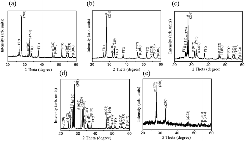 |
| | Fig. 1 XRD patterns of various Bi2O3 films: (a) 10-Bi2O3. (b) 13-Bi2O3. (c) 10S-Bi2O3. (d) 13S-Bi2O3. (e) Sputtering deposited Bi2O3 seed layer. | |
Fig. 2 shows top- and cross-sectional views of SEM micrographs of various Bi2O3 films prepared by various process procedures. In Fig. 2(a), the as-synthesized 10-Bi2O3 film is composed of many nanosheets perpendicular to the substrate surface and crossing each other. These sheet-like structures have the thickness in the range of 40–70 nm and width in the range of 2.5–3.5 μm. The Bi2O3 nanosheets contained numerous tiny pores. Furthermore, the Bi2O3 nanosheets exhibited a rugged peripheral morphology, and the composition is loose from the cross-sectional view observation. By contrast, the 13-Bi2O3 film consisted of numerous plates with a high growth density and shape uniformity as observed in Fig. 2(b). The Bi2O3 plates were in a rectangular morphology and the surface of peripherals was smooth. Comparatively, the distribution density of the Bi2O3 plates over the area of the substrate is substantially higher than that of the 10-Bi2O3 film. From Fig. 2(b), the thickness and width of the plates can be evaluated to be approximately in the ranges of 500–700 nm and 2.5–3.5 μm, respectively. The SEM observations herein demonstrated that the 13-Bi2O3 plates are thicker than that of the 10-Bi2O3 nanosheets, revealing the higher pH reaction solution caused an increased Bi2O3 crystal thickness. This can be understood from earlier eqn (4) that the higher the pH value of the reaction solution, the more the bismuth ion reacts with the hydroxide ion; the thicker Bi(OH)3 will be formed during the CBD. The initially formed thicker Bi(OH)3 crystals will result in formation of the thicker Bi2O3 crystals after the postannealing procedure. Fig. 2(c) and (d) show the SEM images of the 10S-Bi2O3 and 13S-Bi2O3 films grown with the assistance of the homo-Bi2O3 seed layers, respectively. In Fig. 2(c), the Bi2O3 nanosheets grown on the homo-Bi2O3 seed layer showed similar crystal morphology as revealed in Fig. 2(a). Moreover, the size of the nanosheets herein is almost the same with those grown without a homo-Bi2O3 seed layer, but 10S-Bi2O3 nanosheets are more evenly and densely dispersed on the substrate. The Bi2O3 seed layer herein promoted the CBD-derived Bi(OH)3 crystal growth to be more uniformly along the seed layer. By contrast, the 13S-Bi2O3 film exhibited a feathery crystal feature which differed from the 13-Bi2O3 film (Fig. 2(d)). The feathery crystals had a thickness ranged from 1.0–1.5 μm and their length was approximately 3.0–4.0 μm. These feathery crystals were densely contacted to each other; moreover, several feathery crystals are bundled and arranged in a specific crystal orientation. This might be associated with the crystallographic orientation of the homo-seed layer that affect the resultant CBD-derived crystal growth orientation herein. It has also been shown that the homo-WO3 seed layer promotes growth density and orientation of CBD-derived H2WO4·nH2O precursor crystals and therefore, highly oriented and dense WO3 nanostructures are formed after postannealing procedures. Furthermore, a similar promotion of crystal distribution density and consistency of growth orientation from a homoseed layer has been shown in the CBD-derived Fe2O3 and TiO2 oxide crystal growth. The improved growth density and consistency of growth orientation in CBD-derived FeOOH and Ti(OH)4 precursor crystals respectively on the Fe2O3 and TiO2 thin homoseed layers result in formation of dense and highly-oriented Fe2O3 and TiO2 crystals after proper post annealing procedures.25,26 Notably, from earlier XRD analyses, the formation of 13S-Bi2O3 film is related to the crystal structure of monoclinic α-Bi2O3 and tetragonal β-Bi2O3. A markedly higher phase content of α-Bi2O3 in the 13S-Bi2O3 film might explain the observed substantial morphology change of the Bi2O3 film derived from the pH = 13 reaction solution on the homoseed layer. However, this morphology change is not visibly observed for the Bi2O3 film formed from the pH = 10 reaction solution with the assistance of homoseed layer crystal growth. The relative low phase content of α-Bi2O3 in the 10S-Bi2O3 film might not substantially affect its crystal growth mode and the resultant morphology in this study.
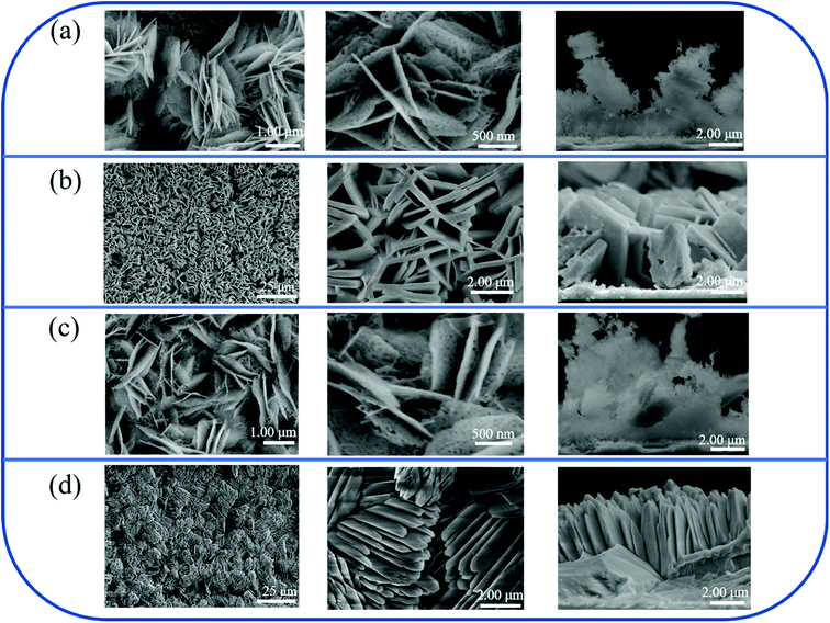 |
| | Fig. 2 SEM top and cross-sectional views of various Bi2O3 films: (a) 10-Bi2O3. (b) 13-Bi2O3. (c) 10S-Bi2O3. (d) 13S-Bi2O3. | |
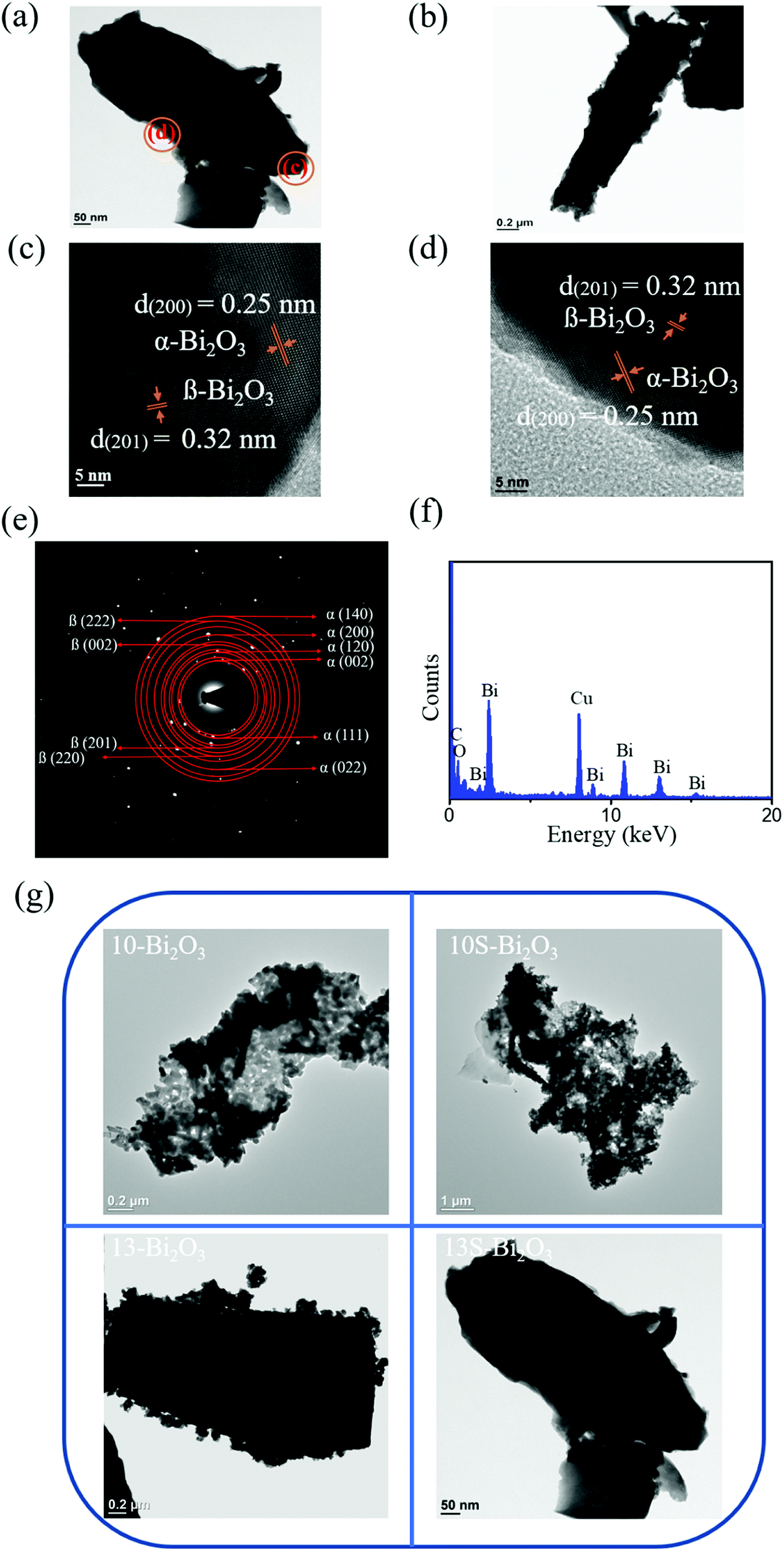
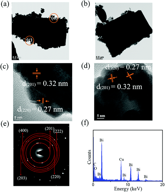
Fig. 3(a) shows a low-magnification TEM image of 10-Bi2O3 nanosheet. The nanosheet exhibited a rugged peripheral morphology. Tiny pores existed in the nanosheet. The nanosheet consisted of many nanoscaled Bi2O3 particles which can be easily distinguished from the grayscale contrast image of particles around the sample. Fig. 3(b) and (c) are high-resolution TEM (HRTEM) images taken from the outer regions of the nanosheet. The visible lattice fringes with multiple orientations are observed in the Bi2O3 nanosheet, which reveals its polycrystalline feature. The distinguishable interplanar spacings of approximately 0.31 nm and 0.27 nm are corresponded to the (201) and (220) planes of tetragonal β-Bi2O3, respectively. Fig. 3(d) displays the selected area electron diffraction (SAED) pattern in which the sharp and bright spots were arranged in concentric circles with various radii. The (201), (002), (220), (222), and (421) crystallographic planes were determined to correspond to the tetragonal β-Bi2O3 phase herein. The composition of the Bi2O3 nanosheet was obtained by energy dispersive spectroscopy (EDS) analysis (Fig. 3(e)); the EDS spectrum indicated that the ratio of Bi/O is approximately 0.71, and the C and Cu signals in the spectrum were originated from the TEM grid.
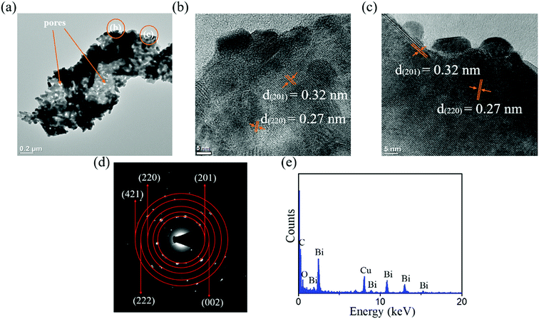 |
| | Fig. 3 TEM analyses of the 10-Bi2O3 film: (a) low-magnification image of 10-Bi2O3 nanosheet. (b and c) High-resolution TEM (HRTEM) images taken from the local regions of the sample in (a). (d) Selected area electron diffraction (SAED) pattern of the sample in (a). (e) Energy dispersive X-ray spectroscopy (EDS) spectrum of the sample in (a). | |
Fig. 4(a) presents a low-magnification TEM image of 10S-Bi2O3 nanosheet. Similar to Fig. 3(a), the nanostructure exhibits sheet morphology with an irregular periphery; moreover, abundant pores existed in the structure. Fig. 4(b) and (c) display HRTEM images taken from the outer regions of the nanosheet. The distinct, ordered lattice fringes with multiple orientations are observed in the nanosheet. The interplanar spacings of approximately 0.32 nm and 0.25 nm are corresponded to the β-Bi2O3 (201) and α-Bi2O3 (200), respectively. HRTEM images reveal well crystalline feature of the nanostructure. The composition of the Bi2O3 nanosheet was further evaluated by EDS spectrum (Fig. 4(d)); the Bi/O ratio of the nanostructure is approximately 0.71 in this study.
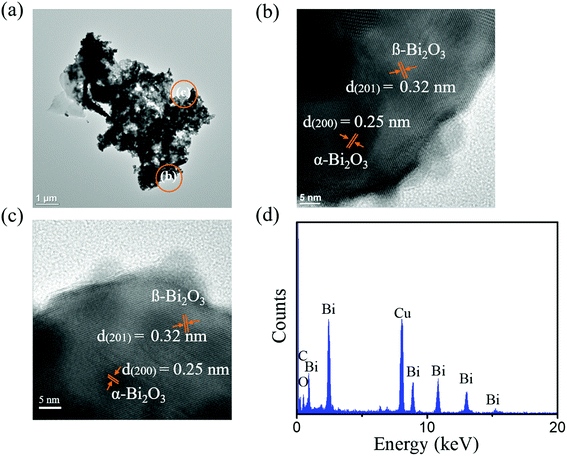 |
| | Fig. 4 TEM analyses of the 10S-Bi2O3 film: (a) low-magnification image of 10S-Bi2O3 nanosheet. (b and c) HRTEM images taken from the local regions of the sample in (a). (d) EDS spectrum of the sample in (a). | |
The low-magnification TEM images in Fig. 5(a) and (b) show that the morphology of the Bi2O3 plates formed at pH = 13 (13-Bi2O3) differed from that of the 10-Bi2O3 nanosheet. The periphery of 13-Bi2O3 plates was relatively flat and the plates were more rectangular shaped. The rectangular 13-Bi2O3 plate was made of Bi2O3 particles with a size of approximately 50 nm and can be observed in these TEM images. These Bi2O3 particles were firmly assembled to form the Bi2O3 plates, and the granular feature is still visibly distinguished on the surface. Fig. 5(c) and (d) are HRTEM images taken from the outer local regions in Fig. 5(a). The clearly lattice fringes with multiple orientations are also observed in the outer regions of the HR images where is the thinner regions of the Bi2O3 plate. The granular particle images can also be distinguished in these HR images. The interplanar spacings with 0.32 nm and 0.27 nm corresponded to the (201) and (220) planes of tetragonal β-Bi2O3, respectively herein. Fig. 5(e) reveals the SAED pattern taken from the selected Bi2O3 plate in Fig. 5(a). The pattern exhibited several distinct diffraction rings consisting of sharp and bright spots that originated from the tetragonal β-Bi2O3 (201), (220), (222), (400), and (203) crystallographic planes. A well crystalline quality of the Bi2O3 plate was formed in this study. The EDS spectrum taken from the Bi2O3 plate (Fig. 5(f)), revealing that the atomic ratio of Bi/O is 0.69.
 |
| | Fig. 5 TEM analyses of the 13-Bi2O3 film: (a and b) low-magnification images of the 13-Bi2O3 plates. (c and d) HRTEM images taken from the local regions of the sample in (a). (e) SAED pattern of the sample in (a). (f) EDS spectrum of the sample in (a). | |
Fig. 6(a) and (b) show the low-magnification images of the 13S-Bi2O3 feathery crystals. The feathery crystals are in a cone shape with two different aspect ratios can be observed herein. The granular particle assembled surface feature of the 13-Bi2O3 plate was not easily observed in Fig. 6(a) and (b). Comparatively, the 13S-Bi2O3 feathery crystals exhibited dense and flat surface feature. Fig. 6(c) and (d) display HRTEM images taken from the outer region of the feathery crystal in Fig. 6(a). Notably, the lattice fringes are quite regularly arranged and are visibly distinguishable at the corner regions. The lattice spacings with 0.32 nm and 0.25 nm corresponded to the (201) plane of β-Bi2O3 and the (200) plane of α-Bi2O3, respectively. The result further confirmed that a phase junction between α-Bi2O3 and β-Bi2O3 was obtained in the 13S-Bi2O3 feather crystal.27 Fig. 6(e) shows the SAED pattern of the 13S-Bi2O3 feathery crystal in Fig. 6(a). According to the SAED pattern, the (201), (002), (220), and (222) crystallographic planes were determined to correspond to the tetragonal β-Bi2O3 phase. Moreover, the (002), (111), (120), (200), (022) and (140) crystal planes corresponded to the monoclinic α-Bi2O3 phase were also identified in the SAED pattern. The SAED analysis revealed that the α- and β-Bi2O3 phases coexisted in the 13S-Bi2O3 film. The EDS spectrum in Fig. 6(f) supported the high composition purity of the as-synthesized, and the Bi/O atomic ratio is approximately 0.68. Finally, a TEM morphology comparison chart of various Bi2O3 crystals was summarized in Fig. 6(g), the effect of homoseed layer on the morphology evolution is especially profound in the CBD-derived Bi2O3 crystals synthesized at pH = 13 reaction solution.
 |
| | Fig. 6 TEM analyses of the 13S-Bi2O3 film: (a and b) low-magnification images of the 13S-Bi2O3 plates. (c and d) HRTEM images taken from the local regions of the sample in (a). (e) SAED pattern of the sample in (a). (f) EDS spectrum of the sample in (a). (g) A summarized TEM morphology chart of various Bi2O3 crystals. | |
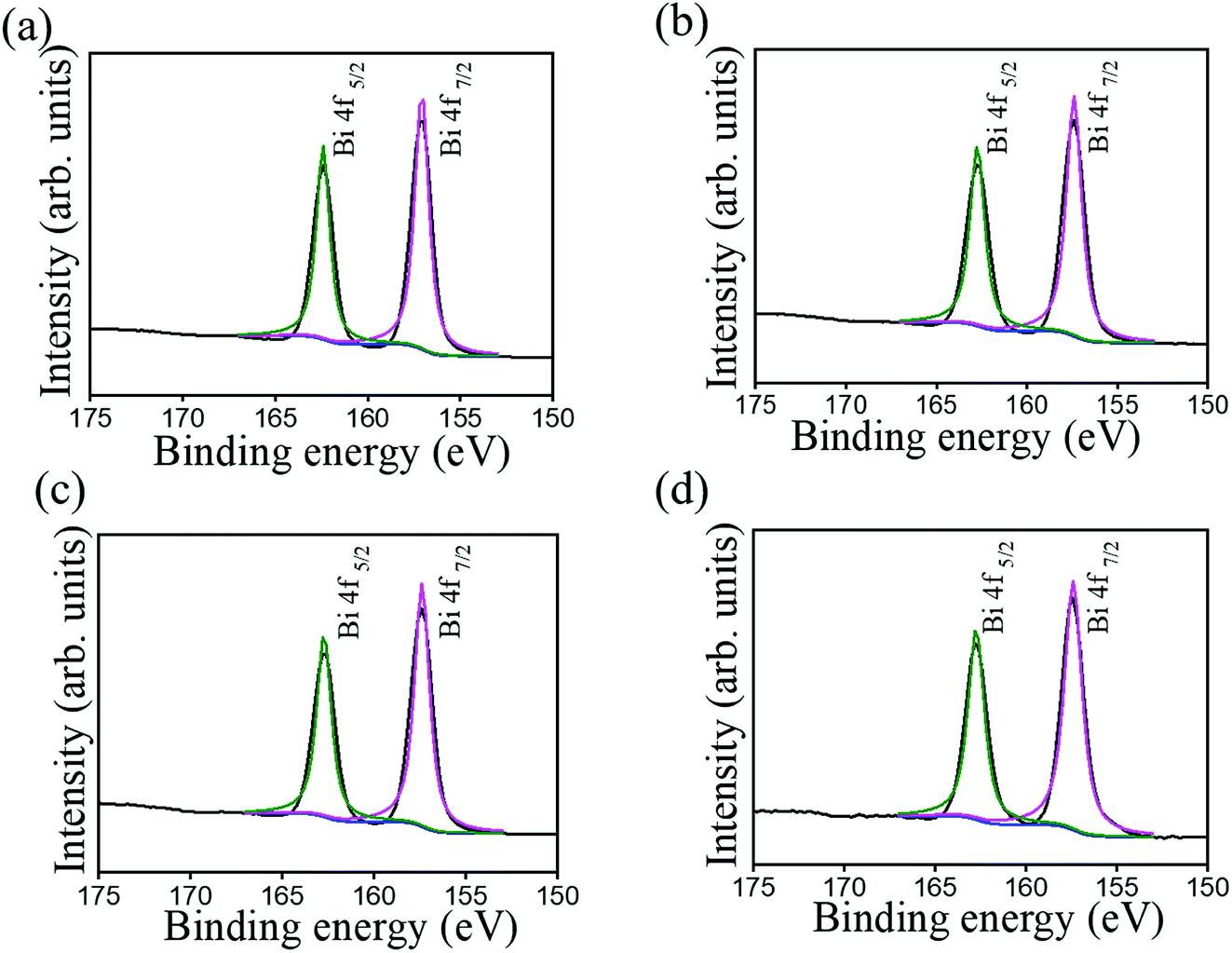
Fig. 7 shows typical XPS survey spectra of various Bi2O3 films. In these XPS survey spectra, the main binding feature peaks can be assigned to originate from Bi, and O, proving the purity of the prepared Bi2O3 sample. Notably, the existence of carbon signal in XPS survey spectra is associated with the exposure of samples to ambient air, engendering surface carbon contamination. Fig. 8 shows the high-resolution XPS spectra of Bi 4f taken from various Bi2O3 films. The Bi 4f7/2 peak at 157.1 eV and Bi 4f5/2 at 162.4 eV could be observed with a separation of 5.3 eV, which was a characteristic of Bi3+ in Bi2O3 crystals according to the previous report.4 No distinct shoulder peaks appeared in Bi 4f spectra, revealing bismuth was only in +3 oxidation state, and no +5 and metallic states are present in the as-synthesized Bi2O3 films.28 Fig. 9 presents the high-resolution O 1s spectra. The asymmetric XPS spectra of the O 1s could be deconvoluted into two subpeaks, which were oxygen in the lattice (Bi–O) at approximately 528.1 eV (peak I) and surface-absorbed oxygen at 529.5 eV (peak II).4 Comparatively, Fig. 9(a) and (c) demonstrate the size of the subpeak at the higher binding energy is higher than that of Fig. 9(b) and (d). This revealed that the surface-absorbed oxygen content of the 10-Bi2O3 and 10S-Bi2O3 films is larger than that of the 13-Bi2O3 and 13S-Bi2O3 films. An increased pH value of the CBD reaction solution to grow Bi2O3 films decreased the surface-absorbed oxygen size of the Bi2O3 thin films accordingly. The relative surface-absorbed oxygen content in the crystalline Bi2O3 films was further evaluated according to the intensity area ratio of Gaussian deconvolution subpeaks: (peak II)/(peak I + peak II). The relative surface-absorbed oxygen contents of the 10-Bi2O3, 13-Bi2O3, 10S-Bi2O3, and 13S-Bi2O3 films are approximately 31.6, 19.8, 33.4, and 23.1%, respectively. We inferred that this diversity may be caused by the different crystal morphology of various Bi2O3 films; more loose and porous structure for the Bi2O3 films synthesized at a lower pH value of the CBD reaction solution might accounted for the observed results.
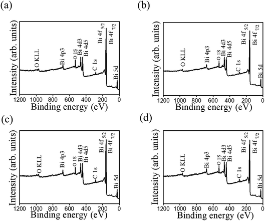 |
| | Fig. 7 XPS survey spectra of various Bi2O3 films: (a) 10-Bi2O3. (b) 13-Bi2O3. (c) 10S-Bi2O3. (d) 13S-Bi2O3. | |
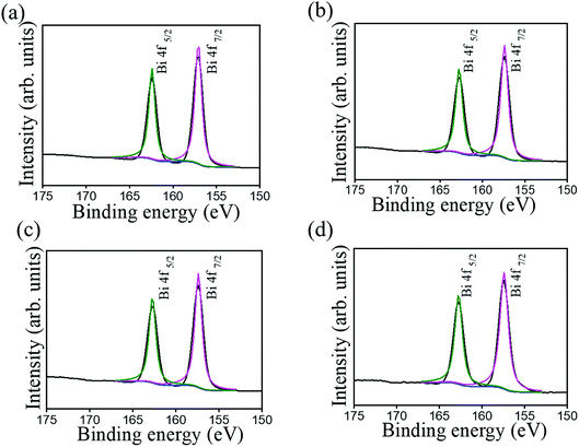 |
| | Fig. 8 High-resolution XPS spectra in the Bi 4f region of various Bi2O3 films: (a) 10-Bi2O3. (b) 13-Bi2O3. (c) 10S-Bi2O3. (d) 13S-Bi2O3. | |
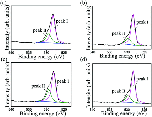 |
| | Fig. 9 High-resolution XPS spectra in the O 1s region of various Bi2O3 films: (a) 10-Bi2O3. (b) 13-Bi2O3. (c) 10S-Bi2O3. (d) 13S-Bi2O3. | |
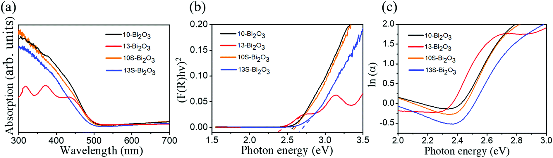
Fig. 10(a) shows the optical absorption properties of various Bi2O3 films. For the 10-Bi2O3 and 13-Bi2O3 films, a sharp drop of the absorption edge was observed, and the onset was at approximately 537 nm, which is consistent with the intrinsic band-gap absorption of tetragonal β-Bi2O3.6 The result shows that β-Bi2O3 films have good absorption in visible light region. The 10-Bi2O3 and 13-Bi2O3 films have the similar absorption range of light wavelength, but the difference in light absorption intensity is very obvious. The 10-Bi2O3 film seems to have significant light utilization efficiency, which might be more effective in photoactive applications. By contrast, 10S-Bi2O3 and 13S-Bi2O3 films have an absorption edge (about 526 nm and 512 nm, respectively) slightly lower than that of the 10-Bi2O3 and 13-Bi2O3 films, respectively. The absorption edges of the 10S-Bi2O3 and 13S-Bi2O3 thin films were between that of pure α-Bi2O3 and β-Bi2O3 phases, indicating that the existence of dual α/β-Bi2O3 phase in the samples.29 Notably, no much difference in the light absorption ability was found for the 10S-Bi2O3 and 10-Bi2O3 thin films; this might be attributed to the fact that the content of α-Bi2O3 crystallite in the 10S-Bi2O3 film is low, and β-Bi2O3 phase still dominated the light absorption property of the 10S-Bi2O3 film. By contrast, the α-Bi2O3 phase content in the 13S-Bi2O3 film was markedly increased to affect the overall light absorption characterization of the 13S-Bi2O3 film. This induced the marked blue-shift of absorption edge of the 13S-Bi2O3 film and resulted in its absorption edge closer to that of pure α-Bi2O3 phase in comparison with that of the 10S-Bi2O3. The optical absorption result of various Bi2O3 films is consistent with the XRD results. The bandgap energy (Eg) was evaluated using the Kubelka–Munk function equation30 and the results are further shown in Fig. 10(b). The bandgap energy of the 10-Bi2O3 and 13-Bi2O3 thin films was 2.5 and 2.43 eV, respectively. These bandgap energies are consistent with the reported values of pure β-Bi2O3 phase.31 Furthermore, the evaluated bandgap energies of the 10S-Bi2O3 (2.53 eV) and 13S-Bi2O3 (2.64 eV) films are between that of reported values of pure α-Bi2O3 and β-Bi2O3,32 which is in agreement with the aforementioned discussions. Notably, Urbach energy corresponds to the width of localized states, and it is used to characterize the disorder degree in crystalline material systems. Fig. 10(c) shows that the absorption coefficient near the absorption edge has an exponential behavior and obeys the empirical Urbach rule33 given by
| |
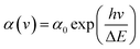 | (6) |
where
α0 is a constant and Δ
E is the Urbach energy. A large Urbach energy would have greater tendency to convert weak bonds into defects. This is evident from the experimental observations of the correlation between the defect density and Urbach energy in the ZnO and TiO
2.
16,34 The evaluated Urbach energies of the 10-Bi
2O
3, 13-Bi
2O
3, 10S-Bi
2O
3 and 13S-Bi
2O
3 films are approximately 0.2078, 0.1254, 0.2263 and 0.1723 eV, respectively. It is found that the Urbach energy of the Bi
2O
3 films formed at pH = 10 is generally greater than the Bi
2O
3 films formed at pH = 13. This is attributable to the fact that the Bi
2O
3 films formed at the reaction solution with a lower pH value resulted in the intermediate stage formed Bi(OH)
3 precursor crystals with a porous and loose structure. This may increase the possibility of initial crystal defects in the prepared Bi
2O
3 thin films after the postannealing procedure in this study.
 |
| | Fig. 10 (a) UV-vis absorption spectra of various Bi2O3 films. (b) Evaluation of band gap of various Bi2O3 films. (c) Urbach energy plots of various Bi2O3 films. | |
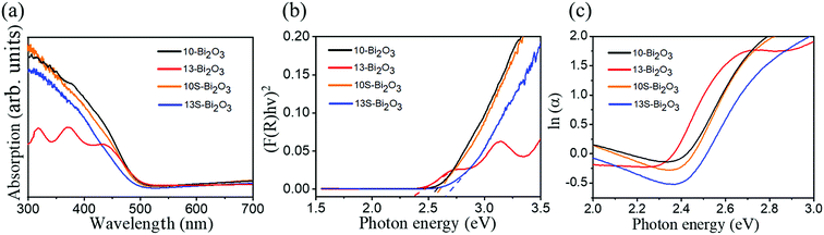
The morphology effect on electrochemically active surface area (ECSA) size of porous (10-Bi2O3 and 10S-Bi2O3) and solid (13-Bi2O3 and 13S-Bi2O3) Bi2O3 films are further investigated; the relevant results provide overall electro-catalytic activity of the Bi2O3 electrode materials.35 The ECSA of the 10-Bi2O3, 13-Bi2O3,10S-Bi2O3, and 13S-Bi2O3 films was compared through the values of electrochemical double-layer capacitance (Cdl) because the Cdl is positively proportional to ECSA of the sample.36 Fig. 11(a)–(d) show cyclic voltammetry (CV) curves at non-faradaic potential regions (−0.2–0.2 V vs. NHE) with different scan rates for various Bi2O3 films. All the Bi2O3 films showed the rectangular CV curves and peak separation took place with scanning speed from 0.1 to 0.5 V s−1. Notably, the 10-Bi2O3 and 10S-Bi2O3 films exhibited the higher current density at the constant potential than did the 13-Bi2O3 and 13S-Bi2O3 films. The double-layer charging current (Δj) is equal to ja − jc, in which ja is anodic current and jc is cathodic current at the middle potential (0 V) against the CV scan rate. The correlation between the double-layer charging current and electrochemical double-layer capacitance follows Δj = vCdl, in which v is the scan rate.37 A plot of Δj as a function of v yields a straight line with a slope equal to Cdl value of the Bi2O3 film (Fig. 11(e)). According to Fig. 11(e), the Cdl values of 10-Bi2O3 and 10S-Bi2O3 thin films are closed to be 0.024 mF cm−2 and 0.027 mF cm−2, respectively. This is associated with the similar morphology of the 10-Bi2O3 and 10S-Bi2O3 films through earlier SEM observations. By contrast, the 13-Bi2O3 and 13S-Bi2O3 films exhibited smaller Cdl values of approximately 0.008 mF cm−2 and 0.013 mF cm−2, respectively. The Cdl value of the Bi2O3 films formed at pH = 10 is almost 2–3 times higher than that of the Bi2O3 films formed at pH = 13 herein. Thus, the ECSA of the four Bi2O3 films follows the trend 10S-Bi2O3 > 10-Bi2O3 > 13S-Bi2O3 > 13-Bi2O3. The higher ECSA of the 10S-Bi2O3 and 10-Bi2O3 films herein revealed more surface active sites exposed during electrochemical measurements and maintained a sufficient electrochemical reaction between thin-film electrode and electrolyte ions. This thus might deliver improved photo-/electrocatalytic performance of the 10-Bi2O3 and 10S-Bi2O3 films in comparison with that of the 13-Bi2O3 and 13S-Bi2O3 films.38 The morphology effect on electrochemical active of various as-synthesized Bi2O3 films with and without a porous structure is visibly demonstrated herein.
 |
| | Fig. 11 Cyclic voltammetry curves of various Bi2O3 thin-film electrodes measured at the non-faradaic region of −0.20–0.20 V vs. NHE with different scan rates, varying from 0.1–0.5 V s−1: (a) 10-Bi2O3. (b) 10S-Bi2O3. (c) 13-Bi2O3. (d) 13S-Bi2O3. (e) Scan rate dependent current density curves of various Bi2O3 thin-film electrodes. | |
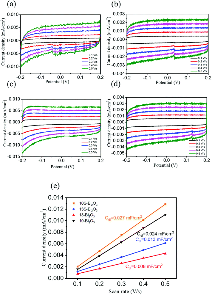
Fig. 12(a) shows transient photoresponse curves of various Bi2O3 films. The Bi2O3 films exhibited perfect switching behavior under the chopping visible light irradiation. Notably, all the Bi2O3 photoelectrodes showed clear spike-like transient response. The possible cause of this spike transient feature is associated with the recombination of the photoinduced electrons and holes at the surface states of the oxides.39,40 The maximum steady-state photocurrent density value achieved by the Bi2O3 photoelectrodes under irradiation follows the order: 10S-Bi2O3 > 10-Bi2O3 > 13S-Bi2O3 > 13-Bi2O3. The photocurrent densities of the 10-Bi2O3 and 13-Bi2O3 photoelectrodes with a pure β-Bi2O3 phase are 0.0039 mA cm−2 and 0.0012 mA cm−2, respectively. Comparatively, 10S-Bi2O3 and 13S-Bi2O3 photoelectrodes with a dual α/β-Bi2O3 phase showed markedly enhanced photocurrent density under irradiation with respect to that of the 10-Bi2O3 and 13-Bi2O3 photoelectrodes, respectively. The maximum steady-state photocurrent densities of the 10S-Bi2O3 and 13S-Bi2O3 photoelectrodes are approximately 0.0078 mA cm−2 and 0.0034 mA cm−2, respectively; these photocurrent densities are around 2 and 3 times higher than that of the 10-Bi2O3 and 13-Bi2O3 photoelectrodes, respectively. Notably, the 10S-Bi2O3 photoelectrode achieved the highest photocurrent density in this study. The significant increase in photocurrent density of the Bi2O3 photoelectrode under irradiation indicates the improved separation ability of photogenerated electron (e−)–hole (h+) pairs in semiconductor oxides.2,3 The transient photocurrent density vs. time curves results herein demonstrated that the 10S-Bi2O3 photoelectrode exhibited the superior photoinduced electron–hole separation efficiency among various Bi2O3 photoelectrodes. Notably, the photocurrent density of the Bi2O3 photoelectrodes with a dual α/β-Bi2O3 phase is significantly higher than that of the Bi2O3 photoelectrodes with a pure β-Bi2O3 phase under the similar synthesis solution pH value but with and without seed layer assisted growth, indicating that the α/β homojunction is effective to separate the photoinduced electron–hole pairs.2,41 This is related to the proper type II energy band arrangement between α-Bi2O3 and β-Bi2O3, which markedly enhances photoinduced charge separation efficiency in the polymorphic Bi2O3 film.2 It is worth noting that 10-Bi2O3 photoelectrode has better photoresponse performance than did 13S-Bi2O3 thin-film photoelectrode. One possible reason can be explained by the porous structure of the 10-Bi2O3 film observed earlier. The Bi2O3 films with a porous structure could lead to a larger specific surface area which contributed to more favorable adsorption of OH− over the surfaces and lead to an improved light harvesting ability of the porous film compared with the solid one.42 The aforementioned both reasons can explain the higher photoactive performance of the 10-Bi2O3 photoelectrode than that of the 13S-Bi2O3 photoelectrode. Fig. 12(b) shows the Nyquist plots of various Bi2O3 photoelectrodes under irradiation. Small semi-circular radii are typically attributed to photoelectrodes that exhibit small charge-transfer resistance; moreover, due to the small charge transfer resistance, there will be a higher separation efficiency of photogenerated electrons and holes in material systems.2,16 From Fig. 12(b), the semi-circular radii of the Bi2O3 photoelectrodes with a seed layer assisted crystal growth were smaller than those of the Bi2O3 photoelectrodes prepared under the same process condition but without a Bi2O3 seed layer assisted growth, indicating that the charge-transfer resistance of the Bi2O3 films was substantially improved via a seed layer assisted crystal growth during CBD. The earlier mentioned coexistence of α/β-Bi2O3 phases in the 10S-Bi2O3 and 13S-Bi2O3 photoelectrodes might explain their lower internal charge transfer resistance than that of the 10-Bi2O3 and 13-Bi2O3 photoelectrodes, respectively. The relatively lower internal charge transfer resistance can accelerate electron transfer and inhibit photoinduced electron/hole recombination.43 Comparatively, the Nyquist plot radius of the 10S-Bi2O3 photoelectrode was the smallest among various Bi2O3 photoelectrodes. The multiple factors associated with a thin layer morphology, high porosity, good light-capturing ability, and coexistence of α/β-Bi2O3 phases might accounted for the observed results herein. Fig. 12(c) exhibits the possible equivalent circuits for a quantitative analysis of interfacial charge transfer ability of various Bi2O3 photoelectrodes. As the illustrations shown, the solution resistance Rs depends on the concentration and conductivity of the electrolyte.44 The C is an ordinary double layer capacitance for the electrode surface.45 Rct represents the electron transfer resistance, and it can be estimated through the fitting of arc radii of the Nyquist curves. Rct (α) is a charge transfer resistance across the formed α-Bi2O3 electrolyte interface, and C (α) is an ordinary double layer capacitance for the formed α-Bi2O3 surface.46 In the current work, the separately evaluated Rct values of the 10-Bi2O3, 13-Bi2O3, 10S-Bi2O3, and 13S-Bi2O3 are approximately 1000, 6369, 618 and 1196 ohm. Overall, the PEC and EIS results herein behaved that the Bi2O3 films with a dual α/β-Bi2O3 phase (10S-Bi2O3 and 13S-Bi2O3) exhibited superior charge separation and transportation efficiencies, in turn reduced the interfacial resistance in comparison with that of their counterparts (10-Bi2O3 and 13-Bi2O3).
 |
| | Fig. 12 (a) Transient photocurrent density versus time curves of various Bi2O3 photoelectrodes under chopped illumination at 1 V. (b) Nyquist plots of various Bi2O3 photoelectrodes under visible light irradiation. (c) The possible equivalent circuit used for Rct evaluation of various Bi2O3 photoelectrodes. | |
To understand the origin of the enhanced PEC activity in the α/β-Bi2O3 composite photoelectrodes, the Mott–Schottky plots of various Bi2O3 films are measured (Fig. 13(a)–(d)). The Mott–Schottky plots of various Bi2O3 films with a positive slope indicated the n-type characteristic with electron conduction.47 The Mott–Schottky plot according to the slope in the quasi-linear region of Fig. 13(a) indicated that the flat band potential of 10-Bi2O3 is around 0.48 eV (vs. normal hydrogen electrode, NHE). The flat-band potential of 13-Bi2O3 is estimated at 0.49 eV (Fig. 13(b)). In general, the conduction band (CB) potentials are more negative by about −0.1 eV than the flat potentials for n-type semiconductors.48,49 The CB potentials of 10-Bi2O3 and 13-Bi2O3 are evaluated to be approximately 0.38 eV and 0.39 eV, respectively. Moreover, according to the earlier bandgap energy results of the Bi2O3 films, the VB potentials of 10-Bi2O3 and 13-Bi2O3 could be calculated as 2.88 eV and 2.82 eV (vs. NHE) according to the equation ECB = EVB − Eg, respectively, which also match well with the values in the literature.50,51 Notably, 10S-Bi2O3 and 13S-Bi2O3 are polymorphic structures (dual α/β-Bi2O3 phases), the position of the conduction band cannot be known from the current Mott–Schottky plots, so they are not further discussed. The flat band potentials of 10S-Bi2O3 and 13S-Bi2O3 in Fig. 13(c) and (d) are between the reported reference values of the α-Bi2O3 and β-Bi2O3 phases,41 supporting a α-Bi2O3/β-Bi2O3 junction existed in the 10S-Bi2O3 and 13S-Bi2O3 thin films. Furthermore, the carrier density of the oxide semiconductor is inversely proportional to the slope of the straight-line portion in the Mott–Schottky plot according to the proposed relationship of 1/C2 versus the applied potential.52 The tangent slope size in Fig. 13(a)–(d) shows the order: 10S-Bi2O3 < 10-Bi2O3 < 13S-Bi2O3 < 13-Bi2O3. It is evidently that an increased charge carrier density was found in the 10S-Bi2O3 and 13S-Bi2O3 films than that of their counterparts without a seed layer assisted growth. This result might indicate that the formation of α-β homojunction in the Bi2O3 film could efficiently create a sufficient space charge layer to enhance the charge carrier transportation in comparison with that of a pure β-Bi2O3 thin film. Fig. 13(e) shows possible energy band diagram of the 10-Bi2O3 and 13-Bi2O3 films with a pure β-Bi2O3 phase according to the earlier analysis results. By contrast, for the 10S-Bi2O3 and 13S-Bi2O3 thin films in which dual α/β-Bi2O3 phases existed in the films, their homojunction energy band diagrams were constructed with the assistance of α-Bi2O3 energy band diagram from literatures.29 A possible schematic for visible-light-driven electron–hole separation and transport at the homojunction interface of both 10S-Bi2O3 and 13S-Bi2O3 is shown in Fig. 13(e). Since the CB edge potential of α-Bi2O3 is more negative than that of β-Bi2O3, the photoinduced electrons on the CB of the α-Bi2O3 will transfer easily to the CB of the β-Bi2O3 via the well-developed interface. Similarly, the photoinduced holes on the VB of the β-Bi2O3 move to the VB of the α-Bi2O3 due to the large difference in VB edge potentials retarding the recombination of the photoinduced electron–hole pairs in the α/β-Bi2O3 heterojunction of the 10S-Bi2O3 and 13S-Bi2O3 films. Thus, the formation of the α-Bi2O3 phase in the β-Bi2O3 matrixed film via a seed layer assisted growth could function as traps to capture the photoinduced holes and the homojunction of α/β-Bi2O3 could act as an active center for hindering the rapid recombination of photoinduced electron–hole pairs. For the reasons mentioned above, it is known that 10S-Bi2O3 and 13S-Bi2O3 will enhance the charge separation and thus the enhanced PEC and EIS performance in comparison with their counterparts of the 10-Bi2O3 and 13-Bi2O3, respectively.
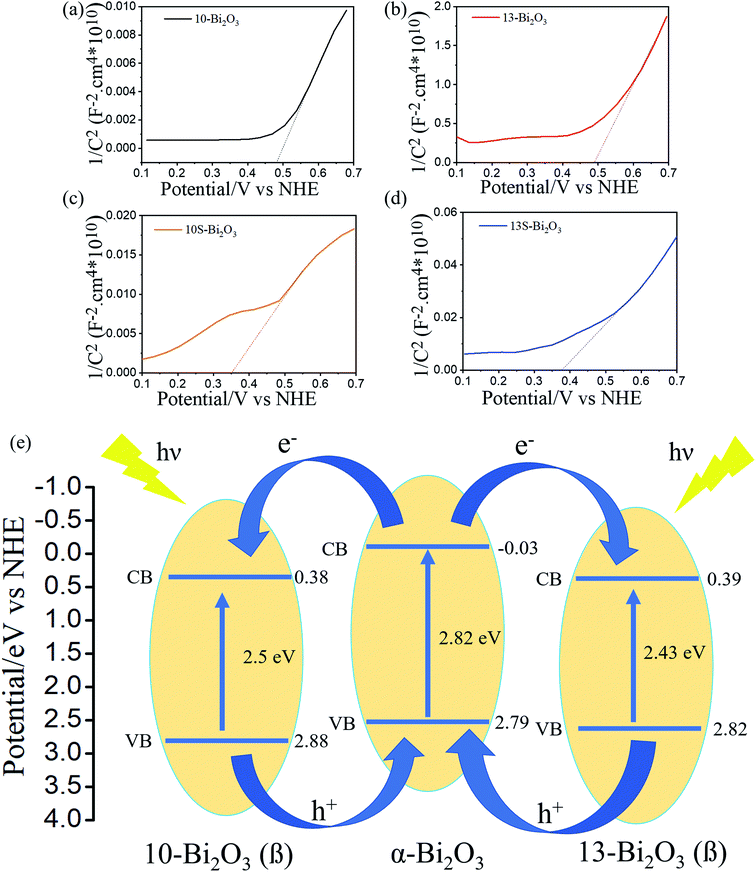 |
| | Fig. 13 Mott–Schottky plots of various Bi2O3 photoelectrodes: (a) 10-Bi2O3 (b) 13-Bi2O3. (c) 10S-Bi2O3. (d) 13S-Bi2O3. (e) Possible photogenerated electron–hole pathways between two polymorphic Bi2O3 semiconductors (α-Bi2O3 and β-Bi2O3) in this study. | |
Conclusions
In summary, the porous β-Bi2O3 nanosheets and solid β-Bi2O3 plates were successfully synthesized by CBD routes with reaction solution of pH = 10 and pH = 13, respectively. These β-Bi2O3 crystals were vertically aligned on the substrates with a high crystallinity. The use of sputter coated α/β-Bi2O3 homoseed layer during CBD crystal growth shows an important effect on the resultant crystallographic structures of the CBD-derived Bi2O3 under the similar processes conditions. The sputter coated α/β-Bi2O3 homoseed layer induced formation of α-Bi2O3 phase in the β-Bi2O3 matrix during the CBD crystal growth. The PEC and EIS results show that the photoactive performance of the CBD-derived Bi2O3 crystals is enhanced via a homoseed layer crystal growth engineering. The proper type II band alignment between α-Bi2O3 and β-Bi2O3 phase improved the efficiency of photoinduced charge separation in the seed layer assisted grown Bi2O3 crystals. Moreover, the porous structure of the Bi2O3 nanosheets formed at a lower pH value of reaction solution improved their specific surface area size and light-trapping performance; therefore, the porous α/β-Bi2O3 nanosheets demonstrated the highest photoactive performance in this study. The porous and dual phase Bi2O3 nanosheets synthesized herein may have the potential for applications in photoactive devices.
Conflicts of interest
There are no conflicts to declare.
Acknowledgements
This research was funded by Ministry of Science and Technology of Taiwan. Grant No. MOST 108-2221-E-019-034-MY3.
References
- Q. Wang, S. Yu, Z. Tan, R. Zhang, Z. Li, X. Gao, B. Shen and H. Su, Synthesis of monodisperse Bi2O3-modified CeO2 nanospheres with excellent photocatalytic activity under visible light, CrystEngComm, 2015, 17, 671–677 Search PubMed.
- Y.-C. Liang and K.-J. Chiang, Growth temperature-dependent phase evolution and photoactivities of sputtering-deposited crystalline Bi2O3 thin films, CrystEngComm, 2020, 22, 4215–4227 Search PubMed.
- Y.-C. Liang and K.-J. Chiang, Coverage Layer Phase Composition-Dependent Photoactivity of One-Dimensional TiO2–Bi2O3 Composites, Nanomaterials, 2020, 10, 1005–1018 Search PubMed.
- H. Cheng, B. Huang, J. Lu, Z. Wang, B. Xu, X. Qin, X. Zhang and Y. Dai, Synergistic effect of crystal and electronic structures on the visible-light-driven photocatalytic performances of Bi2O3 polymorphs, Phys. Chem. Chem. Phys., 2010, 12, 15468–15475 Search PubMed.
- Y.-C. Wu, Y.-T. Huang and H.-Y. Yang, Crystallization mechanism and photocatalytic performance of vanadium-modified bismuth oxide through precipitation processes at room temperature, CrystEngComm, 2016, 18, 6881–6888 Search PubMed.
- Y. Qiu, M. Yang, H. Fan, Y. Zuo, Y. Shao, Y. Xu, X. Yang and S. Yang, Nanowires of α- and β-Bi2O3: phase-selective synthesis and application in photocatalysis, CrystEngComm, 2011, 13, 1843–1850 Search PubMed.
- Y. Xiong, M. Wu, J. Ye and Q. Chen, Synthesis and luminescence properties of hand-like α-Bi2O3 microcrystals, Mater. Lett., 2008, 62(8–9), 1165–1168 Search PubMed.
- A. M. Abu-Dief and W. S. Mohamed, α-Bi2O3 nanorods: synthesis, characterization and UV-photocatalytic activity, Mater. Res. Express, 2017, 4(3), 035039 Search PubMed.
- L. Liu, J. Jiang, S. Jin, Z. Xia and M. Tang, Hydrothermal synthesis of β-bismuth oxide nanowires from particles, CrystEngComm, 2011, 13, 2529–2532 Search PubMed.
- M. Jalalah, M. Faisal, H. Bouzid, J.-G. Park, S. A. Al-Sayari and A. A. Ismail, Comparative study on photocatalytic performances of crystalline α- and β-Bi2O3 nanoparticles under visible light, J. Ind. Eng. Chem., 2015, 30, 183–189 Search PubMed.
- H. Liu, M. Luo, J. Hu, T. Zhou, R. Chen and J. Li, β-Bi2O3 and Er3+ doped β-Bi2O3 single crystalline nanosheets with exposed reactive {0 0 1} facets and enhanced photocatalytic performance, Appl. Catal., B, 2013, 140–141, 141–150 Search PubMed.
- S. Anandan, G.-J. Lee, P.-K. Chen, C. Fan and J. J. Wu, Removal of Orange II Dye in Water by Visible Light Assisted Photocatalytic Ozonation Using Bi2O3 and Au/Bi2O3 Nanorods, Ind. Eng. Chem. Res., 2010, 49(20), 9729–9737 Search PubMed.
- C. Wang, C. Shao, L. Wang, L. Zhang, X. Li and Y. Liu, Electrospinning preparation, characterization and photocatalytic properties of Bi2O3 nanofibers, J. Colloid Interface Sci., 2009, 333(1), 242–248 Search PubMed.
- S. Kong, Z. An, W. Zhang, Z. An, M. Yuan and D. Chen, Preparation of Hollow Flower-Like Microspherical β-Bi2O3/BiOCl Heterojunction and High Photocatalytic Property for Tetracycline Hydrochloride Degradation, Nanomaterials, 2020, 10(1), 57 Search PubMed.
- X. Huang, C. Tan, Z. Yin and H. Zhang, 25th Anniversary Article: Hybrid Nanostructures Based on Two-Dimensional Nanomaterials, Adv. Mater., 2014, 26(14), 2185–2204 Search PubMed.
- Y.-C. Liang, C.-S. Hung and W.-C. Zhao, Thermal Annealing Induced Controllable Porosity and Photoactive Performance of 2D ZnO Sheets, Nanomaterials, 2020, 10(7), 1352–1366 Search PubMed.
- Z. Zhang, D. Jiang, C. Xing, L. Chen, M. Chen and M. He, Novel AgI-decorated β-Bi2O3 nanosheet heterostructured Z-scheme photocatalysts for efficient degradation of organic pollutants with enhanced performance, Dalton Trans., 2015, 44(25), 11582–11591 Search PubMed.
- Y. Wang, L. Jiang, D. Tang, F. Liu and Y. Lai, Characterization of porous bismuth oxide (Bi2O3) nanoplates prepared by chemical bath deposition and post annealing, RSC Adv., 2015, 5(80), 65591–65594 Search PubMed.
- Y. Yin, Y. Sun, M. Yu, X. Liu, B. Yang, D. Liu, S. Liu, W. Cao and M. N. R. Ashfold, Controlling the hydrothermal growth and the properties of ZnO nanorod arrays by pre-treating the seed layer, RSC Adv., 2014, 4(48), 44452–44456 Search PubMed.
- Y.-C. Liang and C.-S. Hung, Effects of sputtering deposited homoseed layer microstructures on crystal growth behavior and photoactivity of chemical route-derived WO3 nanorods, CrystEngComm, 2019, 21, 5779–5788 Search PubMed.
- C. Zhu and M. J. Panzer, Seed Layer-Assisted Chemical Bath Deposition of CuO Films on ITO Coated Glass Substrates with Tunable Crystallinity and Morphology, Chem. Mater., 2014, 26(9), 2960–2966 Search PubMed.
- T. P. Gujar, V. R. Shinde, C. D. Lokhande, R. S. Mane and S.-H. Han, Bismuth oxide thin films prepared by chemical bath deposition (CBD) method: annealing effect, Appl. Surf. Sci., 2005, 250(1–4), 161–167 Search PubMed.
- K. Barrera-Mota, M. Bizarro, M. Castellino, A. Tagliaferro, A. Hernández and S. E. Rodil, Spray deposited β-Bi2O3 nanostructured films with visible photocatalytic activity for solar water, Photochem. Photobiol. Sci., 2015, 14(6), 1110–1119 Search PubMed.
- X. Y. Chen, H. S. Huh and S. W. Lee, Controlled synthesis of bismuth oxo nanoscale crystals (BiOCl, Bi12O17Cl2, α-Bi2O3, and (BiO)2CO3) by solution-phase methods, J. Solid State Chem., 2007, 180(9), 2510–2516 Search PubMed.
- D.-D. Qin, C.-L. Tao, Z.-Y. Yang, T. E. Mallouk, N. Bao and C. A. Grimes, Facile Solvothermal Method for Fabricating Arrays of Vertically Oriented α-Fe2O3 Nanowires and Their Application in Photoelectrochemical Water Oxidation, Energy Fuels, 2011, 25(11), 5257–5263 Search PubMed.
- A. M. Selman and Z. Hassan, Influence of deposition temperature on the growth of rutile TiO2 nanostructures by CBD method on seed layer prepared by RF magnetron sputtering, Superlattices Microstruct., 2013, 64, 27–36 Search PubMed.
- Y. Shi, L. Luo, Y. Zhang, Y. Chen, S. Wang, L. Li, Y. Long and F. Jiang, Synthesis and characterization of α/β-Bi2O3 with enhanced photocatalytic activity for 17α-ethynylestradiol, Ceram. Int., 2017, 43(10), 7627–7635 Search PubMed.
- D. Barreca, F. Morazzoni, G. Andrea Rizzi, R. Scotti and E. Tondello, Molecular oxygen interaction with a spectroscopic and Bi2O3 : spectromagnetic investigation, Phys. Chem. Chem. Phys., 2001, 3(9), 1743–1749 Search PubMed.
- Y. Ma, Q. Han, T.-W. Chiu, X. Wang and J. Zhu, Simple thermal decomposition of bismuth citrate to Bi/C/α-Bi2O3 with enhanced photocatalytic performance and adsorptive ability, Catal. Today, 2018, 340, 40–48 Search PubMed.
- Y.-C. Liang and T.-W. Lung, Growth of Hydrothermally Derived CdS-Based Nanostructures with Various Crystal Features and Photoactivated Properties, Nanoscale Res. Lett., 2016, 11(1), 264 Search PubMed.
- T. A. Gadhi, S. Hernández, M. Castellino, P. Jagdale, T. Husak, A. Hernández-Gordillo, A. Tagliaferro and N. Russo, Insights on the role of β-Bi2O3/Bi5O7NO3 heterostructures synthesized by a scalable solid-state method for the sunlight-driven photocatalytic degradation of dyes, Catal. Today, 2018, 321, 135–145 Search PubMed.
- D. Chen, S. Wu, J. Fang, S. Lu, G. Zhou, W. Feng, Y. Fan, Y. Chen and Z. Fang, A nanosheet-like α-Bi2O3/g-C3N4 heterostructure modified by plasmonic metallic Bi and oxygen vacancies with high photodegradation activity of organic pollutants, Sep. Purif. Technol., 2018, 193, 232–241 Search PubMed.
- F. Urbach, The Long-Wavelength Edge of Photographic Sensitivity and of the Electronic Absorption of Solids, Phys. Rev., 1953, 92(5), 1324 Search PubMed.
- B. Choudhury and A. Choudhury, Oxygen defect dependent variation of band gap, Urbach energy and luminescence property of anatase, anatase–rutile mixed phase and of rutile phases of TiO2 nanoparticles, Phys. E, 2014, 56, 364–371 Search PubMed.
- B. Qin, H. Yu, X. Gao, D. Yao, X. Sun, W. Song, B. Yi and Z. Shao, Ultrathin IrRu nanowire networks with high performance and durability for the hydrogen oxidation reaction in alkaline anion exchange membrane fuel cells, J. Mater. Chem. A, 2018, 6, 20374–20382 Search PubMed.
- H. Hu, B. Guan, B. Xia and X. W. Lou, Designed Formation of Co3O4/NiCo2O4 Double-Shelled Nanocages with Enhanced Pseudocapacitive and Electrocatalytic Properties, J. Am. Chem. Soc., 2015, 137(16), 5590–5595 Search PubMed.
- C. C. L. McCrory, S. Jung, J. C. Peters and T. F. Jaramillo, Benchmarking Heterogeneous Electrocatalysts for the Oxygen Evolution Reaction, J. Am. Chem. Soc., 2013, 135(45), 16977–16987 Search PubMed.
- Y. Tang, X. Fang, X. Zhang, G. Fernandes, Y. Yan, D. Yan, X. Xiang and J. He, Space-confined earth-abundant bifunctional electrocatalyst for high-efficiency water splitting, ACS Appl. Mater. Interfaces, 2017, 9(42), 36762–36771 Search PubMed.
- Y.-C. Liang and C.-S. Hung, Design of Hydrothermally Derived Fe2O3 Rods with Enhanced Dual Functionality Via Sputtering Decoration of a Thin ZnO Coverage Layer, ACS Omega, 2020, 5, 16272–16283 Search PubMed.
- A. Watanabe and H. Kozuka, Photoanodic Properties of Sol–Gel-Derived Fe2O3 Thin Films Containing Dispersed Gold and Silver Particles, J. Phys. Chem. B, 2003, 107(46), 12713–12720 Search PubMed.
- J. Hou, C. Yang, Z. Wang, W. Zhou, S. Jiao and H. Zhu, In situ synthesis of α–β phase heterojunction on Bi2O3 nanowires with exceptional visible-light photocatalytic performance, Appl. Catal., B, 2013, 142–143, 504–11 Search PubMed.
- X. Yang, X. Lian, S. Liu, C. Jiang, J. Tian, G. Wang, J. Chen and R. Wang, Visible light photoelectrochemical properties of β-Bi2O3 nanoporous films: a study of the dependence on thermal treatment and film thickness, Appl. Surf. Sci., 2013, 282, 538–543 Search PubMed.
- H. Huang, K. Xiao, K. Liu, S. Yu and Y. Zhang, In Situ Composition-Transforming Fabrication of BiOI/BiOIO3 Heterostructure: Semiconductor p–n Junction and Dominantly Exposed Reactive Facets, Cryst. Growth Des., 2015, 16(1), 221–228 Search PubMed.
- M. Ahila, E. Subramanian and D. Pathinettam Padiyan, Influence of annealing on phase transformation and specific capacitance enhancement in Bi2O3, J. Electroanal. Chem., 2017, 805, 146–158 Search PubMed.
- N. F. Atta, A. H. Ibrahima and A. Galal, Nickel oxide nanoparticles/ionic liquid crystal modified carbon composite electrode for determination of neurotransmitters and paracetamol, New J. Chem., 2016, 40, 662–673 Search PubMed.
- L. Shan, G. Wang, D. Li, X. San, L. Liu, L. Dong and Z. Wu, Band alignment and enhanced photocatalytic activation of α/β-Bi2O3 heterojunctions via in situ phase transformation, Dalton Trans., 2015, 44(17), 7835–7843 Search PubMed.
- H.-Y. Wang, J. Chen, F.-X. Xiao, J. Zheng and B. Liu, Doping-induced structural evolution from rutile to anatase: formation of Nb-doped anatase TiO2 nanosheets with high photocatalytic activity, J. Mater. Chem. A, 2016, 4(18), 6926–6932 Search PubMed.
- X. Li, J. Yu, J. Low, Y. Fang, J. Xiao and X. Chen, Engineering heterogeneous semiconductors for solar water splitting, J. Mater. Chem. A, 2015, 3(6), 2485–2534 Search PubMed.
- X. Yue, S. Yi, R. Wang, Z. Zhang and S. Qiu, A novel architecture of dandelion-like Mo2C/TiO2 heterojunction photocatalysts towards highperformance photocatalytic hydrogen production from water splitting, J. Mater. Chem. A, 2017, 5(21), 10591–10598 Search PubMed.
- K. K. Bera, M. Chakraborty, M. Mondal, S. Banik and S. K. Bhattacharya, Synthesis of α-β Bi2O3 heterojunction photocatalyst and evaluation of reaction mechanism for degradation of RhB dye under natural sunlight, Ceram. Int., 2019, 46(6), 7667–7680 Search PubMed.
- A. Lebedev, F. Anariba, X. Li, D. Seng Hwee Leng and P. Wu, Rational design of visible-light-driven Pd-loaded α/β-Bi2O3 nanorods with exceptional cationic and anionic dye degradation properties, Sol. Energy, 2019, 190, 531–542 Search PubMed.
- H. Farsi, S. Moghiminia, A. Roohi and S.-A. Hosseini, Preparation, characterization and electrochemical behaviors of Bi2O3 nanoparticles dispersed in silica matrix, Electrochim. Acta, 2014, 148, 93–103 Search PubMed.
|
| This journal is © The Royal Society of Chemistry 2020 |
Click here to see how this site uses Cookies. View our privacy policy here. 
 Open Access Article
 This Open Access Article is licensed under a Creative Commons Attribution-Non Commercial 3.0 Unported Licence
 * and
Yu-Hsun Chou
* and
Yu-Hsun Chou