
 Open Access Article
 This Open Access Article is licensed under a Creative Commons Attribution-Non Commercial 3.0 Unported Licence
A novel fabrication technique for high-aspect-ratio nanopillar arrays for SERS application
Tianli Duan *a,
Chenjie Gub,
Diing Shenp Angc,
Kang Xud and
Zhihong Liue
*a,
Chenjie Gub,
Diing Shenp Angc,
Kang Xud and
Zhihong Liue
aSUSTech Core Research Facilities, Southern University of Science and Technology, 1088 Xueyuan Avenue, Shenzhen 518055, China. E-mail: duantl@sustech.edu.cn
bInstitute of Photonics, Ningbo University, 818 Feng Hua Road, Ningbo 315211, China
cSchool of Electrical and Electronic Engineering, Nanyang Technological University, Nanyang Avenue, Singapore 639798
dDepartment of Mechanical and Energy Engineering, Southern University of Science and Technology, 1088 Xueyuan Avenue, Shenzhen 518055, China
eSchool of Microelectronics, Xidian University, Xian 710071, China
First published on 21st December 2020
Abstract
A novel technique is demonstrated for the fabrication of silicon nanopillar arrays with high aspect ratios. Our technique leverages on an “antenna effect” present on a chromium (Cr) hard mask during ion-coupled plasma (ICP) etching. Randomly distributed sharp tips around the Cr edge act as antennas that attract etchant ions, which in turn enhance the etching of the Cr edge. This antenna effect leads to a smaller Cr mask size and thus a smaller nanopillar diameter. With optimized SF6 and CHF3 gas flow during ICP etching, we could achieve nanopillar arrays with sub-30 nm diameter, over 20 aspect ratio, and steep sidewall without collapse. The proposed technique may help break the limit of traditional nanopillar array fabrication, and be applied in many areas, such as Surface-Enhanced Raman Scattering (SERS). A series of SERS simulations performed on nanopillar arrays fabricated by this technique show an obvious Raman spectrum intensity enhancement. This enhancement becomes more obvious when the diameter of the nanopillar becomes smaller and the aspect ratio becomes higher, which may be explained by a high light absorption, the lightning-rod effect, and a greater number of free electrons available at the surface due to the higher density of the surface state.
Introduction
A nanopillar array has many unique advantages, such as nanometer dimensions with specific optical properties and a large surface-to-volume ratio due to its three-dimensional geometry.1–3 It could enhance the Raman spectrum intensity, allowing Surface-Enhanced Raman Scattering (SERS) to reach ultra-sensitive detection.2,4–6 Moreover, a subwavelength nanopillar could achieve high light absorption.7,8 Therefore, a lot of interesting applications of nanopillar arrays have been researched, such as biomaterials,9 GaN sensors,1 solar cells,7,10,11 photodetectors,5 and so on. Among the various nanopillar arrays, silicon nanopillars have been widely investigated because silicon is an important material in optical and optoelectronic devices, moreover, they can be fabricated with existing silicon processing methods and with low cost.12There are many techniques to fabricate nanopillar arrays, such as photolithography with etching,13 nanoimprinting lithography (NIL),14,15 anodic aluminum oxide (AAO) patterning,16,17 self-assembled particles,18 laser direct writing8 and so on. These methods have fabricated the nanopillar arrays with high aspect ratio, large area, or low fabrication cost. However, these methods could not realize nanopillar arrays with multiple accurate diameters and height, as well as flexible patterns combination.19 Furthermore, with the continuous scaling down in the diameter and increase in the aspect ratio of the nanopillar, these methods could no longer satisfy the requirements of sub-30 nm diameter nanopillar fabrication in the future.20
In this work, we report a novel technique for nanopillar fabrication with a diameter less than 30 nm, an aspect ratio greater than 20, and the fabrication area is not limited. Moreover, nanopillars with multiple diameters could be fabricated at the same time. In our technique, after a pattern is written by electron-beam lithography (EBL), a chromium (Cr) film is deposited to serve as a hard mask during ion-coupled plasma (ICP) etching. An antenna effect occurring at the edge of the Cr results in a smaller hard mask, hence nanopillars with a smaller diameter can be formed subsequently. Since our technique is independent of the substrate material, it could also be applied to other semiconductor materials thus offering promising applications in many areas. In addition, SERS simulations based on the nanopillar arrays fabricated in this article are given to reveal the origin of the Raman spectrum intensity enhancement.
Experiment
In this work, a p-doped silicon wafer was used as the substrate for the demonstration. Samples of dimension 2.5 cm by 2.5 cm were cut from the wafer and used in the process optimization work. The fabrication process started with a standard cleaning procedure involving SC1 (H2O2![[thin space (1/6-em)]](https://www.rsc.org/images/entities/char_2009.gif) :NH4OH:H2O = 1:1:5), SC2 (H2O2:HCl:H2O = 1:1:5), and buffered oxide etchant (BOE, HF:NH4F = 1:7) for metal and organic impurity removal. Then, the sample was rinsed in deionized water, dried by N2 gas and baked at 180 °C for 10 min for surface dehydration. The sample was subsequently coated with a layer of EBL resist, polymethyl methacrylate (PMMA, purchased from Allresist Company) and baked at 150 °C for 3 min. The resist thickness was 130 nm, measured by a spectroscopic ellipsometer (UVISEL, HORIBA). The sample was then transferred into an EBL system chamber (nB5, NanoBeam). After electron-beam exposure with an 80 kV acceleration voltage and a 1 nA beam current, the sample was developed in IPA:MIBK = 3:1 for 2 min and dried using N2 gas. Afterward, a Cr film of 40 nm thickness was deposited on the substrate by electron-beam evaporation. A liftoff process was then carried out by dipping the sample in acetone for 5 min to form the Cr hard mask. After the sample was cleaned using deionized water and dried by N2 gas, it was etched in an ICP system using SF6 and CHF3 gas. Two different etching recipes were used: recipe 1–70 sccm CHF3, 10 sccm SF6 and 300 s etching time; recipe 2–65 sccm CHF3, 13 sccm SF6 and 200 s etching time. Recipe 2 was ran twice, resulting in a total etch time of 400 s. The bias power, ICP power and pressure were 50 W, 150 W and 5 mTorr, respectively. In the samples used for the S2 and S3 mask designs (see later discussion), the bottom was coated with heat conduction oil to reduce the temperature increase during etching. This serves as a comparison with non-coated samples to check the effect of temperature increase on the etching process. Finally, all the samples were investigated in a scanning electron microscope (SEM, ZEISS) with a tilt angle of 45°.
:NH4OH:H2O = 1:1:5), SC2 (H2O2:HCl:H2O = 1:1:5), and buffered oxide etchant (BOE, HF:NH4F = 1:7) for metal and organic impurity removal. Then, the sample was rinsed in deionized water, dried by N2 gas and baked at 180 °C for 10 min for surface dehydration. The sample was subsequently coated with a layer of EBL resist, polymethyl methacrylate (PMMA, purchased from Allresist Company) and baked at 150 °C for 3 min. The resist thickness was 130 nm, measured by a spectroscopic ellipsometer (UVISEL, HORIBA). The sample was then transferred into an EBL system chamber (nB5, NanoBeam). After electron-beam exposure with an 80 kV acceleration voltage and a 1 nA beam current, the sample was developed in IPA:MIBK = 3:1 for 2 min and dried using N2 gas. Afterward, a Cr film of 40 nm thickness was deposited on the substrate by electron-beam evaporation. A liftoff process was then carried out by dipping the sample in acetone for 5 min to form the Cr hard mask. After the sample was cleaned using deionized water and dried by N2 gas, it was etched in an ICP system using SF6 and CHF3 gas. Two different etching recipes were used: recipe 1–70 sccm CHF3, 10 sccm SF6 and 300 s etching time; recipe 2–65 sccm CHF3, 13 sccm SF6 and 200 s etching time. Recipe 2 was ran twice, resulting in a total etch time of 400 s. The bias power, ICP power and pressure were 50 W, 150 W and 5 mTorr, respectively. In the samples used for the S2 and S3 mask designs (see later discussion), the bottom was coated with heat conduction oil to reduce the temperature increase during etching. This serves as a comparison with non-coated samples to check the effect of temperature increase on the etching process. Finally, all the samples were investigated in a scanning electron microscope (SEM, ZEISS) with a tilt angle of 45°.
Results and discussion
Fig. 1(a) shows an example of an EBL mask design (S1) used in our study. The array of red squares is meant to be exposed during the EBL process. Each square has a dimension of 50 nm and a pitch of 500 nm in both x and y directions. After liftoff, the diameter of each quasi-circular Cr mask is around 73 nm, as measured by SEM (Fig. 1(b)). It can be seen from the SEM image that the edge of the Cr mask is not smooth but has some protrusions. After ICP etch with recipe 1, the diameter of the nanopillars is around 25 nm and the etched depth is around 702 nm. The nanopillars have steep sidewalls and a high aspect ratio of about 28, as shown in Fig. 1(c). It may be deduced that the size of the Cr mask was decreased during ICP etching, since the nanopillars have a smaller diameter than the initial mask.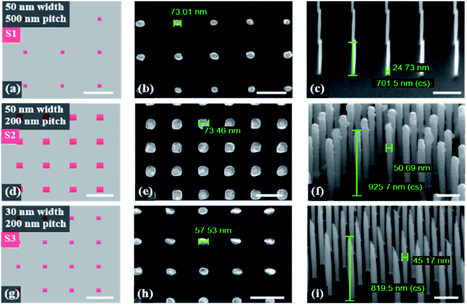 | ||
| Fig. 1 The etching results for three EBL mask designs (S1–S3); each is an array of squares of a particular dimension and pitch (equal in both x and y directions). (a)–(c) present, respectively the S1 mask design (50 nm squares and 500 nm pitch), SEM of the Cr masks after liftoff and nanopillar arrays of diameter ∼25 nm and height ∼702 nm after ICP etch. (d)–(f) present the S2 mask design (50 nm squares and 200 nm pitch), Cr mask SEM and etched nanopillars, respectively. (g) shows the S3 mask design (30 nm squares and 200 nm pitch) and (h) and (i) show the respective Cr mask SEM and etched nanopillars. All figures have a scale bars of 200 nm and “cs” means actual dimension after considering the 45° tilted view. | ||
Similar to S1, nanopillars having a diameter smaller than the Cr masks were obtained using another mask design S2 with 50 nm squares and 200 nm pitch (Fig. 1(d)). After liftoff, the Cr mask size is around 73 nm. After etching with recipe 2, the nanopillar diameter is around 50 nm, which is about 50% smaller than the mask size. The nanopillars likewise have very steep sidewall and tall height (925 nm); the aspect ratio is around 18. Another mask design S3 (Fig. 1(g)) also yielded similar results (Fig. 1(h) and (i)). After liftoff, the Cr mask size is around 60 nm, as shown in Fig. 1(h). After ICP etch using recipe 2, the diameter of the nanopillar is around 45 nm and the etched depth is around 820 nm, giving an aspect ratio of about 18 (Fig. 1(i)). It is noticed that the Cr was almost etched away during ICP etching, resulting in needle-like nanopillars. The results for S1–S3 are summarized in Table 1.
| Mask design | Etching recipe | Designed mask | After liftoff | After etching | Aspect ratio | Etching rate | |||
|---|---|---|---|---|---|---|---|---|---|
| Width (nm) | Pitch (nm) | Cr size (nm) | Diameter (nm) | Height (nm) | Cr (nm s−1) | Silicon (nm s−1) | |||
| S1 | Recipe 1: 70 sccm CHF3, 10 sccm SF6, 300 s | 50.00 | 500.00 | 73.01 | 24.73 | 701.50 | 28.37 | 0.16 | 2.34 |
| S2 | Recipe 2: 65 sccm CHF3, 13 sccm SF6, 400 s (ran twice with 200 s each; heat conductor oil used) | 50.00 | 200.00 | 73.46 | 50.69 | 925.70 | 18.26 | 0.06 | 2.31 |
| S3 | 30.00 | 200.00 | 57.53 | 45.17 | 819.50 | 18.14 | 0.14 | 2.05 | |
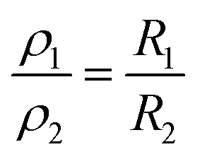
The difference between the Cr mask size after liftoff and the diameter of the resultant nanopillars after etching may be explained by the reduction in mask size caused by edge roughness. Fig. 2(a) provides a schematic illustration. In the depicted Cr mask, the curvature R1 at location 1 is larger than the curvature R2 at another location 2, i.e. the mask edge at location 1 is sharper than that at location 2. The relationship between curvature R and metal charge density ρ may be expressed as follows:
 | (1) |
 | ||
| Fig. 2 A schematic depiction of the antenna effect caused by sharp edges on a Cr mask during ICP etching. (a) More positive ions are attracted to the sharper edge at location 1 (antenna effect), enhancing the etching of the mask at this location. (b) A schematic diagram showing equipotential contour lines around the Cr mask, with a closer line spacing or higher electric field at the sharper edge. (c) Due to the antenna effect, a smaller Cr mask with a smoother edge is obtained. | ||
Since R1 > R2, ρ1 > ρ2, the corresponding electric field at location 1 is higher than that at location 2 (Fig. 2(b)). Consequently, more plasma ions (i.e. CHF2+, SF5+) are attracted to location 1 than location 2, resulting in a higher etch rate at the former. As the etching progresses, a smoother and smaller Cr mask is thus achieved (Fig. 2(c)). Since more substrate area is exposed to the plasma etch, this results in nanopillars with a smaller diameter than the original Cr mask.
The estimated etch rate of the Cr mask is given in Table 1. For the S1 mask design, the width of the Cr mask is decreased from 73.01 nm to 24.73 nm within 300 s. The estimated average etch rate is 0.16 nm s−1. As for the S2 mask design, the width of the Cr mask is decreased from 73.46 nm to 50.69 nm within 400 s, giving an estimated average etch rate of 0.06 nm s−1. With the same etching recipe 2, the Cr mask in S3 design was completely etched away in the same period. In addition to the 40 nm Cr thickness, two other thicknesses, namely 100 nm and 30 nm were also studied. For the 100 nm Cr thickness, “shrinkage” of the Cr mask is not obvious, so the diameter of the nanopillar is not decreased. As for the much thinner 30 nm Cr thickness, the Cr masks were etched away quickly, resulting in needle-like nanopillars. These observations suggest that besides the etch recipe, the Cr mask etching rate is increased as the size and thickness of the Cr mask are decreased. Moreover, the lower silicon rate of S3 is because the top of the nanopillar might be etched after the Cr mask was completely etched away, giving a lower pillar height.
Because the size of the Cr mask is gradually decreasing during etching, the nanopillar formation should be affected accordingly. With more area exposed to the ions as the mask size decreases, the top of the nanopillar should be narrower than the bottom, i.e. an inclined sidewall would be expected. However, the nanopillars achieved in our work all have steep sidewalls. This may be ascribed to the much larger substrate etch rate (more than 10 times that of the Cr mask etch rate), accomplished by etch recipe optimization.
In silicon etching, it is known that SF6 is the main etchant while CHF3 is for sidewall protection. A higher SF6 flow rate would yield a greater etch depth whereas a higher CHF3 flow rate would give a more vertical sidewall. In our work, we studied two recipes. As shown in Table 1, the SF6 flow rate for recipe 1 is 10 sccm, lower than the 13 sccm of recipe 2. Even though recipe 2 has a higher SF6 flow rate and was ran twice, resulting in a total etch time of 400 s (longer than the 300 s for recipe 1) and a larger etch depth of 925 nm (versus 702 nm for recipe 1), the Cr mask size reduction (from 73.46 nm to 50.69 nm or a change of 22.77 nm) is visibly lesser than that of recipe 1 (from 73.01 nm to 24.73 nm or a change of 48.28 nm). The much lower Cr-mask etch rate of sample S2, compared to in sample S1, may be ascribed to the smaller temperature increase of the former during etching, since the bottom of the sample was coated with heat conduction oil.
In the case of sample S3, the Cr mask was completely removed during etching (cf. Fig. 1(i)), resulting in needle-like nanopillars, and the estimated Cr-mask etch rate is comparable to that of sample S1 (albeit could be slightly underestimated since the Cr mask might have been completely etched away before the end of the 2nd run of recipe 2). The higher Cr-mask etch rate of S3 than S2 may be caused by the smaller Cr mask size.
These observations indicate that besides varying the ratio of SF6 and CHF3, controlling the temperature during etching and thus the rate of Cr mask size-reduction provides an additional means for achieving uniform nanopillars with high aspect ratio. The Cr mask size reduction during etching is a crucial consideration and a lack of precise control may yield nanopillars with a deformed top after complete removal of the mask by the etching process.
In order to investigate the SERS performance of the Si nanopillar arrays fabricated by this technique, the simulation of electric field enhancement is demonstrated below. The finite-difference time-domain (FDTD) method was adopted for the simulation and MATLAB was used to process the data. The FDTD simulation was carried out on an array of nine nanopillars and was based on a normal model with perfectly matching layer (PML) boundary condition along the plane perpendicular to the z direction and periodic boundary condition on the sidewall. The incident polarized light was applied along the x direction, with its intensity E0 kept constant. The simulation model is schematically depicted in the inset of Fig. 3(a). The Si substrate is shown as the light blue region while the nanopillars are denoted by the dark blue regions. The translucent area refers to the incident light and the red arrow indicates the light polarization direction parallel to the x axis.
 | ||
| Fig. 3 Simulated electric field enhancement in the fabricated nanopillar arrays. (a) Electric field enhancement strengths of three different nanopillar arrays (modeled after samples S1–S3). The inset is a schematic diagram of the simulated 3 × 3 nanopillar arrays; the red arrow refers to the direction of light polarization. (b) Electric field in the vertical and horizontal sections of a nanopillar (modeled after sample S1) at 266 nm wavelength. (c and d) Electric field enhancement (@266 nm wavelength) in nanopillar arrays with 200 nm and 500 nm pitches, respectively as a function of nanopillar diameter and height. | ||
Generally, the electric field enhancement strength ISERS is proportional to (E/E0)4.3 In Fig. 3(a), the (E/E0)4 parameter of nanopillars having diameter and height similar to those achieved experimentally for samples S1–S3 are shown as a function of wavelengths. As can be seen, the nanopillars perform better in the short wavelength regime. The simulated sample S1, whose nanopillars have the smallest diameter and the largest aspect ratio, exhibits a relatively smooth curve. Fig. 3(b) presents the electric field in the vertical and horizontal sections of a nanopillar in the simulated sample S1 at a wavelength of 266 nm. This wavelength is chosen because it is widely used21 and the fabricated nanopillars perform better at this wavelength, as observed from Fig. 3(a). The enhancement happens near the nanopillar and along the direction of light polarization, due to the stimulation of the fundamental HE11 mode.2 As observed from Fig. 3(b), the hotspot is more than one along the nanopillar.22 It is because the lightning-rod effect between the neighboring nanopillar and the localized surface plasmon resonance field intensity increased significantly.22,23 Fig. 3(c) and (d) show the (E/E0)4 parameter for nanopillar arrays with a pitch of 200 nm and 500 nm, respectively. Various nanopillar diameters (24.73 nm, 45.17 nm, 50.69 nm) and heights (700 nm, 800 nm, 900 nm), similar to those obtained experimentally for samples S1–S3 are examined. As can be seen, the electric field enhancement increases significantly when the diameter of the nanopillars is decreased.
As we know, the enhancement mechanism of the silicon nanopillar is complex.2,11 Because it is related with the wavelength of light, light absorption ratio, the lightning-rod effect, the high aspect ratio of nanopillar, and the propagation of energy along the nanowires.8,22,23 In this article, after the nanopillar is etched by the ICP, the surface of the subwavelength nanopillar is rough and has some sharp edges along the nanopillar. Therefore, surface states, such as dangling bonds and defects, could induce states into the bandgap and improve the surface conductivity, thus more free electrons are generated and involve into the surface plasmon resonance.24 Moreover, ordered nanopillar array with high aspect ratio could achieve high absorption, so the plasmon resonance could be enhanced accordingly.7,8 In addition, surfaces with sharp curvatures could concentrate electromagnetic field further, known as lightning-rod effect.23 Based on this effect, the plasmon resonance and the hotspot density is increased, thus the electric field is enhanced.23,25 Therefore, SERS signal is enhanced significantly for the nanopillar with a smaller diameter and a high aspect ratio.
Conflicts of interest
There are no conflicts of interest to declare.Acknowledgements
The research was founded by Shenzhen Science and Technology Creation Commission, “Research and application on high dense nanopillar by electron beam lithography” (Grant No. JCYJ20170817105420497).References
- Y. D. Wang, S. J. Chua, S. Tripathy, M. S. Sander, P. Chen and C. G. Fonstad, High optical quality GaN nanopillar arrays, Appl. Phys. Lett., 2005, 86(7), L1059 Search PubMed
.
- S. M. Wells, I. A. Merkulov, I. I. Kravchenko, N. V. Lavrik and M. J. Sepaniak, Silicon nanopillars for field-enhanced surface spectroscopy, ACS Nano, 2012, 6(4), 2948–2959 Search PubMed
- N. P. Reddy, S. Naureen, F. Wang, K. Vora, N. Shahid, F. Karouta, H. H. Tan and C. Jagadish, Fabrication and photoluminescence studies of GaN nanopillars, in 2014 Conference on Optoelectronic and Microelectronic Materials & Devices, 14-17 Dec. 2014, 2014, pp. 133–135 Search PubMed
- Z. Huang, G. Meng, Q. Huang, Y. Yang, C. Zhu and C. Tang, Improved SERS Performance from Au Nanopillar Arrays by Abridging the Pillar Tip Spacing by Ag Sputtering, Adv. Mater., 2010, 22(37), 4136–4139 Search PubMed
- P. Senanayake, C. H. Hung, J. Shapiro, A. Lin, B. Liang, B. S. Williams and D. L. Huffaker, Surface Plasmon-Enhanced Nanopillar Photodetectors, Nano Lett., 2011, 11(12), 5279–5283 Search PubMed
- K. Xu, R. Zhou, K. Takei and M. Hong, Toward Flexible Surface-Enhanced Raman Scattering (SERS) Sensors for Point-of-Care Diagnostics, Adv. Sci., 2019, 1900925 Search PubMed
- E. Garnett and P. Yang, Light Trapping in Silicon Nanowire Solar Cells, Nano Lett., 2010, 10(3), 1082–1087 Search PubMed
- J. Yang, F. Luo, T. S. Kao, X. Li, G. W. Ho, J. Teng, X. Luo and M. Hong, Design and fabrication of broadband ultralow reflectivity black Si surfaces by laser micro/nanoprocessing, Light: Sci. Appl., 2014, 3, 1–8 Search PubMed
- W. Zhao, L. Hanson, H. Y. Lou, M. Akamatsu, P. D. Chowdary, F. Santoro, J. R. Marks, A. Grassart, D. G. Drubin and Y. Cui, Nanoscale manipulation of membrane curvature for probing endocytosis in live cells, Nat. Nanotechnol., 2017, 12, 750–756 Search PubMed
- Z. Fan, D. J. Ruebusch, A. A. Rathore, R. Kapadia, O. Ergen, P. W. Leu and A. Javey, Challenges and prospects of nanopillar-based solar cells, Nano Res., 2009, 2(11), 829–843 Search PubMed
- B. C. P. Sturmberg, K. B. Dossou, L. C. Botten, A. A. Asatryan and R. C. Mcphedran, Modal analysis of enhanced absorption in silicon nanowire arrays, Opt. Express, 2011, 19(suppl 5), A1067 Search PubMed
- K. Seo, M. Wober, P. Steinvurzel, E. Schonbrun, Y. Dan, T. Ellenbogen and K. B. Crozier, Multicolored Vertical Silicon Nanowires, Nano Lett., 2011, 11(4), 1851–1856 Search PubMed
- E. Herth, S. Edmond, D. Bouville, J. L. Cercus and E. Cambril, Micro-/Nanopillars for Micro- and Nanotechnologies Using Inductively Coupled Plasmas, Phys. Status Solidi A, 2019, 216, 1900324 Search PubMed
- C.-W. Kuo, J.-Y. Shiu, Y.-H. Cho and P. Chen, Fabrication of Large-Area Periodic Nanopillar Arrays for Nanoimprint Lithography Using Polymer Colloid Masks, Adv. Mater., 2003, 15(13), 1065–1068 Search PubMed
- K. J. Morton, G. Nieberg, S. Bai and S. Y. Chou, Wafer-scale patterning of sub-40 nm diameter and high aspect ratio (> 50 : 1) silicon pillar arrays by nanoimprint and etching, Nanotechnology, 2008, 19, 345301 Search PubMed
- M. Zhou, X. Xiong, B. Jiang and C. Weng, Fabrication
of high aspect ratio nanopillars and micro/nano combined structures with hydrophobic surface characteristics by injection molding, Appl. Surf. Sci., 2018, 427, 854–860 Search PubMed
- S. Rahman and H. Yang, Nanopillar Arrays of Glassy Carbon by Anodic Aluminum Oxide Nanoporous Templates, Nano Lett., 2003, 3(4), 439–442 Search PubMed
- Y. Ajiki, T. Kan, M. Yahiro, A. Hamada, J. Adachi, C. Adachi, K. Matsumoto and I. Shimoyama, Near infrared photo-detector using self-assembled formation of organic crystalline nanopillar arrays, in 2014 IEEE 27th International Conference on Micro Electro Mechanical Systems (MEMS), 26-30 Jan. 2014, 2014, p. 147 Search PubMed
- N. Li, Y. H. Fu, Y. Dong, T. Hu, Z. Xu, Q. Zhong, D. Li, K. H. Lai, S. Zhu, Q. Lin, Y. Gu and N. Singh, Large-area pixelated metasurface beam deflector on a 12-inch glass wafer for random point generation, Nanophotonics, 2019, 8(10), 1855–1861 Search PubMed
- C. W. Kuo, J. Y. Shiu and P. Chen, Size- and Shape-Controlled Fabrication of Large-Area Periodic Nanopillar Arrays, Chem. Mater., 2003, 15(15), 2917–2920 Search PubMed
- E. Rebollar, S. Pérez, M. Hernández, C. Domingo, M. Martín, T. A. Ezquerra, J. P. García-Ruiz and M. Castillejo, Physicochemical modifications accompanying UV laser induced surface structures on poly(ethylene terephthalate) and their effect on adhesion of mesenchymal cells, Phys. Chem. Chem. Phys., 2014, 16(33), 17551–17559 Search PubMed
- N. Chamuah, G. P. Vaidya, A. M. Joseph and P. Nath, Diagonally Aligned Squared Metal Nano-pillar with Increased Hotspot Density as a Highly Reproducible SERS Substrate, Plasmonics, 2016, 12(5), 1–6 Search PubMed
- N. Fukuoka and K. Tanabe, Lightning-Rod Effect of Plasmonic Field Enhancement on Hydrogen-Absorbing Transition Metals, Nanomaterials, 2019, 9, 1–9 Search PubMed
- U. K. Bhaskar, T. Pardoen, V. Passi and J.-P. Raskin, Surface states and conductivity of silicon nano-wires, J. Appl. Phys., 2013, 113(13), 134502 Search PubMed
- A. Otto, Excitation of nonradiative surface plasma waves in silver by the method of frustrated total reflection, Z. Phys. A: Hadrons Nucl., 1968, 216(4), 398–410 Search PubMed
| This journal is © The Royal Society of Chemistry 2020 |