
 Open Access Article
 This Open Access Article is licensed under a Creative Commons Attribution-Non Commercial 3.0 Unported Licence
Research on laser-assisted selective metallization of a 3D printed ceramic surface
Feng Zhao†
ab,
Chen Jiao†ab,
Deqiao Xieac,
Bin Luab,
Mingbo Qiuab,
Xinyu Yid,
Jiang Liuae,
Changjiang Wangf,
Lida Shen *ab and
Zongjun Tianab
*ab and
Zongjun Tianab
aNational Key Laboratory of Science and Technology on Helicopter Transmission, Nanjing University of Aeronautics and Astronautics, Nanjing 210016, China. E-mail: ldshen@nuaa.edu.cn
bCollege of Mechanical and Electrical Engineering, Nanjing University of Aeronautics and Astronautics, Nanjing 210016, China
cCollege of Energy and Power Engineering, Nanjing University of Aeronautics and Astronautics, Nanjing 210016, China
dInstitute of Electronic Engineering, China Academy of Engineering Physics, Mianyang 621000, China
eDFH Satellite Co., Ltd., Beijing 100094, China
fDepartment of Engineering and Design, University of Sussex, Brighton, BN1 9RH, UK
First published on 11th December 2020
Abstract
In recent years, the question of how to fabricate conductive patterns on complex ceramic surfaces in a high-definition and low-cost manner has been an increasing challenge. This paper presents a complete process chain for the selective metallization of Al2O3 ceramic surfaces based on 3D printing. Laser pre-activation (LPA) is used to “activate” the surface of the ceramic substrate, and then, combined with the electroless copper plating (ECP) process, the Al2O3 substrates can be metalized with preset patterns at room temperature, and a densely packed copper layer with high accuracy and good reproducibility can be obtained. The obtained coating has satisfactory roughness, excellent stability and bonding force, and good solderability. The resistivity of the copper layer measured using a four-probe resistance meter is about 3.1 mΩ cm. The limit line width of the metal circuit is about 33.2 μm. Finally, application cases of precision devices such as antennas with ceramic substrates are prepared. This study opens up a broader space for the design and manufacture of 3D microwave devices.
1. Introduction
With the rapid development of microelectronics technology, the complexity and density of components in electronic devices is increasing. Therefore, the requirements for heat dissipation and insulation of circuit substrates are increasing, especially for power integrated circuit components powered by high current or high voltage.1–4 In addition, with the advent of the 5 G era, new requirements have been issued for the miniaturization of devices, especially millimetre wave antennas and filters.5 Compared with traditional resin-based printed circuit boards, surface metallized Al2O3 ceramics have good thermal conductivity, high electrical resistance, better mechanical strength, and less thermal stress and strain in high-power electrical appliances. Simultaneously, the dielectric constant can be changed by adjusting the ceramics powder ratio. They are thus widely used in the electronics and RF circuit industry, such as high-power LEDs, integrated circuits, and filters.5–9The miniaturization of device may require the original planar layout to be changed to a spatial layout, which requires curved substrates. Traditional ceramic-forming processes, such as film rolling and tape casting, have advantages to produce regular-shaped ceramics such as thin sheets,10–12 but it is more difficult to produce ceramic substrates with complex structures. Nowadays, the realization of ceramic devices with complex structures through additive manufacturing (AM) has become a research hotspot. This includes devices such as ceramic filters and ceramic-based antennas that are widely used in wireless mobile communications, satellite communications, and radar systems.13
Various methods can be used to achieve metallization patterns on ceramics, including magnetron sputtering, screen printing, inkjet printing, and direct bonding copper coating.14–21 Magnetron sputtering uses magnetron technology to deposit multilayer films on the substrate, which has a good reproducibility and substrate adhesion. However, the magnetron sputtering technology requires expensive equipment, it is difficult to deposit thick films due to large internal stress, and the shape cannot be precisely controlled, which hinders its large-scale application. Screen-printing technology can produce a thicker conductive layer by printing conductive paste on the surface, but it has higher requirements for the conductive paste, with problems such as uneven stress, surface burns, and cracks occur during sintering. Because inkjet printing technology is mask-less, it is highly suitable for surface patterning on various substrates, but problems such as the clogging of the nozzles due to the aggregation of nanoparticles in the ink and the uneven morphology of the printed patterns have brought challenges to its further application.
Electroless Copper Plating (ECP) is widely used in the manufacture of integrated circuits and on-board antennas due to its low cost, strong production capacity, and low processing temperature.18,22,23 However, Al2O3 ceramics do not possess catalytic activity, so it must be pre-activated. The traditional Pd activation method of waste-liquid treatment is difficult, polluting, and costly. The process of using nickel and copper as active catalysts has thus been greatly developed. However, the use of activated catalyst technology depends heavily on the formulation of the activator and is not suitable for large-scale applications. The combination of laser pre-activation (LPA) and ECP is an effective method for preparing metal lines on the Al2O3 ceramic surface.
In this paper, LPA and ECP successfully obtained selective metallization patterns on the surface of complex Al2O3 ceramic substrate. This method is simple, economical, and effective; it can easily control the thickness of the copper layer; and the obtained coating has satisfactory roughness, bonding force, stability and good solderability.
2. Experiment
2.1. Preparation of the Al2O3 ceramic substrate
The Al2O3 ceramic substrate used in the experiment was prepared by a self-developed light-curing 3D-printer. The ceramic suspension was mainly composed of Al2O3 powder (Al2O3 ≥ 99.5wt%, Chengdu Kewan Intelligent Technology Co., Ltd, Chengdu, China), photosensitive resin (polyacrylic resin, Shanghai Airui Technology Co., Ltd., Shanghai, China), dispersant (sodium polyacrylate, Hebei Jinghong Chemical Co., Ltd., Hebei, China), and so on. Al2O3 powder is composed of powder of 5 μm particle size and 500 nm particle size. The two kinds of powder sizes were weighed at 1![[thin space (1/6-em)]](https://www.rsc.org/images/entities/char_2009.gif) :1 mass ratio and placed in a planetary ball mill (Changsha Miqi Instrument Equipment Co., Ltd., Hunan, China) to mix. The operation mode was set as positive and negative rotation for 8 h. The 5 μm particle size gives the ceramic slurry good fluidity, while the 500 nm particle size can reduce the surface defects of the sample during debinding and sintering and improve the density.24,25 The photosensitive resin can undergo polymerization, cross-linking and curing reaction between monomers to become solid under 405 nm ultraviolet light. The dispersant can prevent the agglomeration of powders and improve the forming quality. These materials were stirred with a vacuum mixer for 20 minutes, and then the ceramic suspension was placed into the printer cylinder. After the slurry was configured, the sample model designed in the CAD software was imported into the machine for printing. After printing, the ceramic substrate was cleaned with ethanol and placed in the sintering furnace for debinding and sintering. Finally, the required ceramic substrate was obtained.
:1 mass ratio and placed in a planetary ball mill (Changsha Miqi Instrument Equipment Co., Ltd., Hunan, China) to mix. The operation mode was set as positive and negative rotation for 8 h. The 5 μm particle size gives the ceramic slurry good fluidity, while the 500 nm particle size can reduce the surface defects of the sample during debinding and sintering and improve the density.24,25 The photosensitive resin can undergo polymerization, cross-linking and curing reaction between monomers to become solid under 405 nm ultraviolet light. The dispersant can prevent the agglomeration of powders and improve the forming quality. These materials were stirred with a vacuum mixer for 20 minutes, and then the ceramic suspension was placed into the printer cylinder. After the slurry was configured, the sample model designed in the CAD software was imported into the machine for printing. After printing, the ceramic substrate was cleaned with ethanol and placed in the sintering furnace for debinding and sintering. Finally, the required ceramic substrate was obtained.
2.2. Realization of selective metallization
LPA were carried out using a fibre pulse laser (Shenzhen Chuangxin Laser Co., Ltd., Shenzhen, China) with a wavelength of 1064 nm and nominal power of 20 W. The laser beam with a pulse duration of 90 ns was delivered through a set of galvanometric mirrors that allow precise XY movement of the laser beam and focused through a F-theta lens with focal distance of 100 mm. This process was conducted under atmospheric conditions (air and room temperature) using a Gaussian spatial laser beam profile of diameter. The required pattern was drawn on the laser control display, the laser focus adjusted, and then the ceramic substrate selectively irradiated.The main components of the ECP solution were copper sulphate pentahydrate (CuSO4·5H2O) and formaldehyde (HCHO). Complexing agents were mainly glycolic acid (HOCH2COOH) and triethanolamine (C6H15NO3). The stabilizers mainly included 2-mercaptobenzothiazole (C6H4SNCSH); the accelerators mainly included phenanthroline (C12H8N2·H2O). After mixing, the pH of the solution was 11.1, and the solution was dark blue. Sodium hydroxide (NaOH) was added to adjust the pH to 13.1 during use. The laser pre-treated ceramic substrate with a predetermined pattern was put into the ECP solution, and the temperature was maintained at 43.8 °C by heating in a water bath. In the experiment, we used 20 minutes as a time gradient to test the effect of different ECP time on the copper deposition performance. Finally, the obtained sample with copper pattern was immersed in antioxidant JPL-008 (Jemply Electronic Technology Co., Ltd.) for 3–5 minutes and then washed with pure water and dried at 80 °C.
The entire experimental process is shown in Fig. 1.
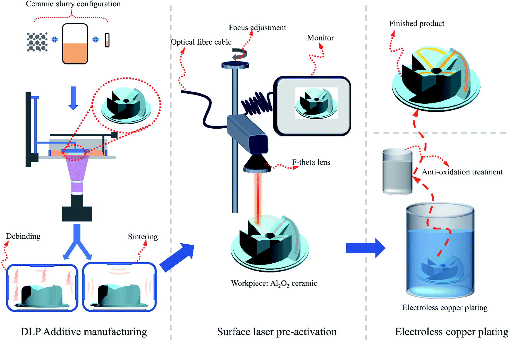 | ||
| Fig. 1 Process flow chart of selective metallization of the Al2O3 ceramic surface. | ||
2.3. Characterization
An optical microscope (CX41, Olympus) and a scanning electron microscope (SEM, Hitachi regulus 8220) were used to check the appearance and surface morphology of the copper plating layer. Energy dispersive X-ray spectroscopy (EDS, Hitachi regulus 8220) was used to analyse the composition of the coating. X-ray diffraction (XRD) technology was used to analyse the composition changes on the ceramic surface after LPA. The resistivity was measured by a four-probe resistance meter (RTS-8). The thickness and surface roughness of the copper layer were measured using a probe contact three-dimensional profiler (Nano-map 500LS) and a non-contact roughness meter (Sensofar Slynx). The coating adhesion automatic scratch tester (WS-2005) was used to measure the bonding force under normal conditions.3. Results and discussion
3.1. Al2O3 ceramic surface pre-activation
The previous papers results show that ECP can be conducted on the surface of Al2O3 ceramics directly after laser treatment without coating activators or sensitizers.26–28 This shows that the laser has changed the reactivity of the ceramic surface. Fig. 2 shows the evolution before and after the laser treatment of the Al2O3 ceramic surface. Before LPA, the SEM image of ceramic surface shows clear and complete grains (Fig. 2a), and the surface roughness is small (Fig. 2b). When the surface is irradiated by laser, the intact grains are destroyed, and the surface shows a large number of micropores and nano-scale particle protrusions (Fig. 2d). The roughness of the ceramic surface changed significantly (Fig. 2e). In addition, the most obvious change is the colour of the ceramic surface. The area after LPA changes from the original white to yellow-grey, and the stronger the laser energy, the darker the colour. This is due to the increased surface roughness and a large number of micropores and particle protrusions on the surface changing the ability of the ceramic surface to absorb light. Through the comparison of XRD in Fig. 2g and h, it is found that no new phases were formed when the Al2O3 ceramic surface was treated by laser. However, we can observe that the diffraction peaks on the surface shift to the right and θ angle becomes larger, which indicates that the crystal lattice may be distorted after LPA. The EDS diagrams of Fig. 2c and f show that after LPA, the ratio of Al to O on the ceramic surface changed, from 30.06:69.94 to 32.77:67.23, which indicates that potential oxygen vacancies are formed. This phenomenon is consistent with the Fig. 2g and h. Activation is attributed to the formation of oxygen defects and the participation of colour-centre electrons, which induce additional electronic states in the band gap of the ceramic substrate.29
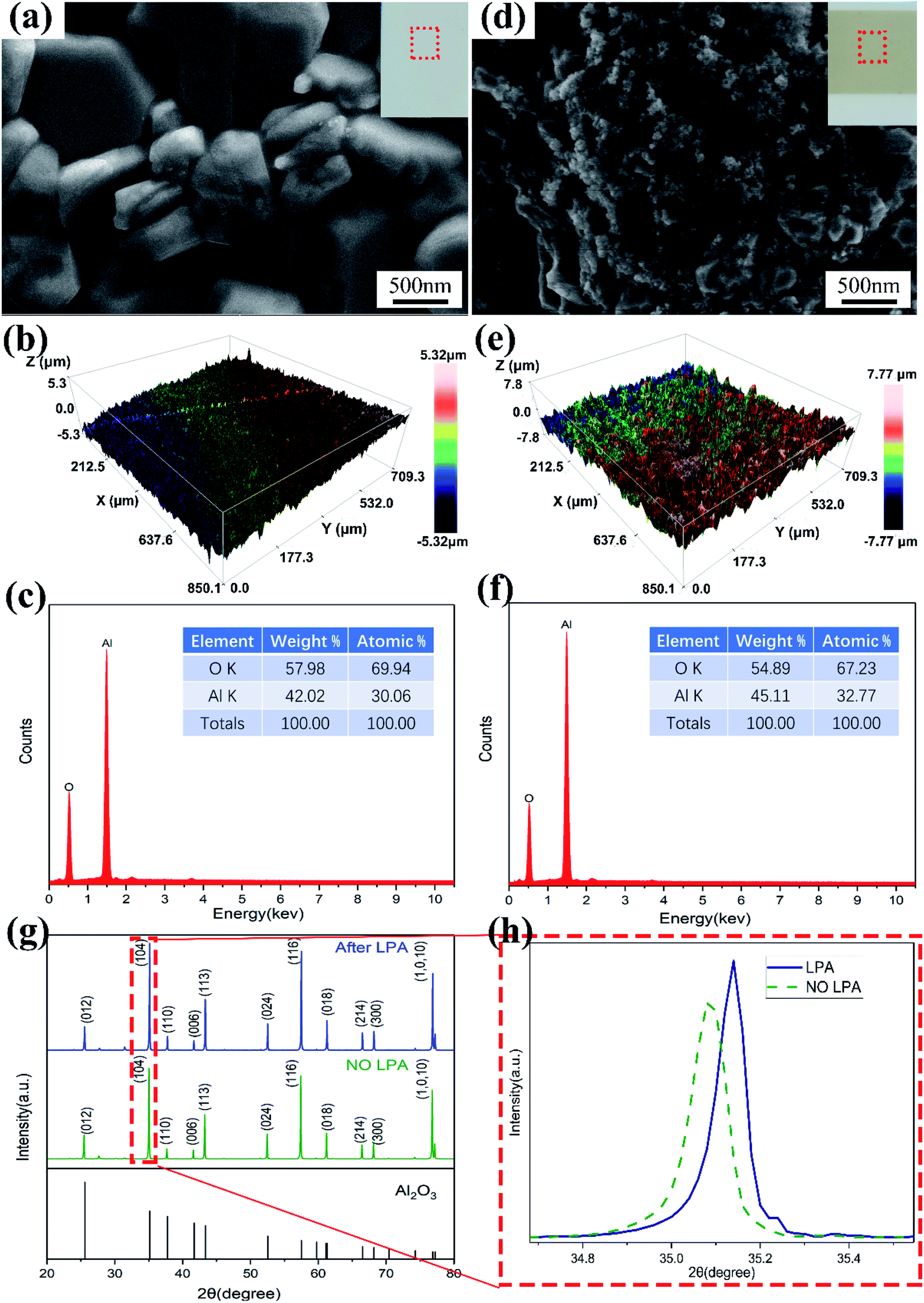 | ||
| Fig. 2 Evolution of Al2O3 ceramic surface with LPA, (a) SEM of ceramic surface before LPA, (b) surface topography before LPA, (c) EDS analysis before LPA, (d) SEM of ceramic surface after LPA, (e) surface topography after LPA, (f) EDS analysis after LPA, (g and h) XRD comparison before and after LPA. | ||
Fig. 3 presents a schematic diagram of the LPA and ECP on the Al2O3 ceramic surface. There were three states of laser irradiation on the ceramic substrate: part of the material vaporized and left the substrate; part of the material burst out of the substrate when melted; the remainder was melted and re-condensed on the substrate.30–32 The superposition of these three states caused the ceramic surface to present micropores and nanoparticle protrusions. These protrusions and micropores formed a “nano-locking” effect, which provided a “target point” for the subsequent ECP. In addition, under the effect of light and heat coupling, point defects appeared on the ceramic surface, forming high-density dislocations or non-chemical ratios to form Al2O3−X and thus forming possible oxygen vacancies. The high-energy or non-chemical composition of dislocation Al2O3−X formed unsaturated bonds on the surface, which changed the original Fermi level and surface activation structure, and enhanced the ceramic surface reaction activity.27,32 This was more conducive to the adsorption of formaldehyde and divalent copper ions in the copper plating solution and reduced the activation energy of the oxidation of formaldehyde to formic acid and the reduction of divalent copper ions to metallic copper, making it easier for redox reactions to occur and catalysing the reaction. Coupled with the “nano-locking” effect resulting from the change in roughness, the ceramic surface could be directly electroless-copper plated without sensitization and activation after the laser treatment.
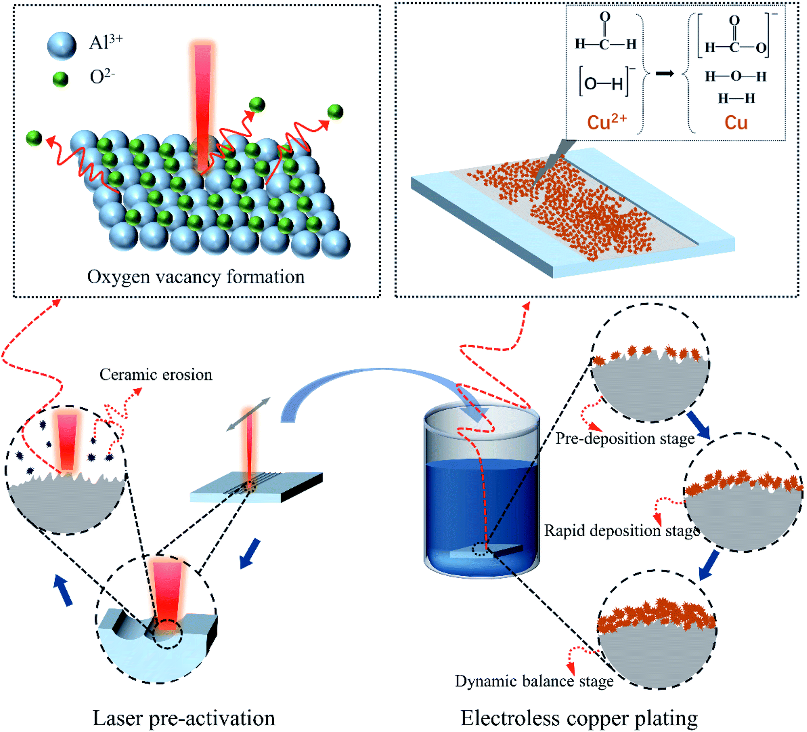 | ||
| Fig. 3 Schematic diagram of laser pre-activation and electroless plating principle. | ||
3.2. Laser parameter analysis
Not all laser irradiation will produce the same effect, Al2O3 ceramics have high temperature resistance, so the laser must meet a certain laser fluence threshold to enable the irradiated ceramics to realize electroless plating activity. When the laser fluence is small, the ceramic surface characteristics change incomplete or unchanged, which will cause the poor coating surface quality. The condition of the coating can be improved by adjusting the parameters of the laser.Fig. 4 shows the parameters of the pulsed laser. The spot diameter used in the experiment was a fixed value of 50 μm, and frequency of 20 kHz. The energy distribution was Gaussian as shown in Fig. 4a. The core area of the spot has high energy and plays a major role. The periphery of the spot was the heat-affected zone. Fig. 4d shows the electroless plating ability of the ceramic surface after LPA with the ECP of 60 min (level 10 is the best, and level 0 is completely ineffective).
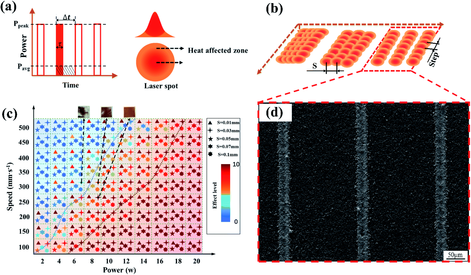 | ||
| Fig. 4 Laser spot and process parameters, (a) Schematic diagram of pulsed laser (Δt: cycle, τ: laser pulse width), (b) schematic diagram of scan spacing, (c) copper plating ability under different process parameters, (d) thin lines with ECP of 60 min. | ||
When the laser fluence is low, the laser scan spacing (S) has a greater impact on the surface pre-treatment. As shown in Fig. 4c, when S was small, the thermal core area of the spot overlapped and it had large transverse pulse overlap. The surface temperature history induced by the first pulse is gradually elevated by the subsequent pulses due to heat accumulation,33 which is equivalent to a secondary treatment of this overlap area, and the pre-activation of the ceramic surface was more reliable. When S was large, it exceeded the spot diameter, and the energy fluence had to be increased to activate the ceramic surface. The result is that the activated area was not continuous, but rather took the form of thin lines. As shown in Fig. 4d, the line width was about 32.2 μm, which is smaller than the spot diameter of 50 μm. This is because the energy of the spot was Gaussian and the core area was about 30 μm. Ultra-fine lines are of great significance to ceramic-based packaging circuits. Similarly, when the laser scanning speed was fast, the step between the front and rear spots became larger, lateral pulse overlap became smaller, the secondary processing area became smaller, and the copper plating effect became worse.
3.3. Analysis of the electroless plating process
When the electroless plating solution is under alkaline conditions, the reaction is shown in the following formula:| Cu2+ + 2HCHO + 4OH− → HCOO− + H2↑ + 2H2O + Cu |
As shown in Fig. 3, according to the changes in the deposition characteristics of the copper layer, the deposition process is divided into three stages. The first is the early pre-deposition stage, characterized by scattered and discontinuous copper deposition, which mainly depends on the micropores on the ceramic surface and the “nano locks” formed by nano bumps. At this stage, the coating defect areas are larger and poorer in quality. The second is the rapid deposition stage, which is characterized by the deposition of gradually denser copper particles, with the copper deposition areas becoming gradually connected and the defect area of the coating gradually becoming smaller. The third is the deposition dynamic balance stage, in which the coating defects almost disappear, the coating quality is better, and the coating is thicker and has good performance.
When the electroless plating time is 15 minutes, as shown in Fig. 5a, it is in the early pre-deposition stage. The deposited copper clusters are distributed, with almost no connection among the clusters. The copper that has been deposited in the first stage becomes a new copper plating “core”, which provides increasingly efficient activation targets for subsequent copper deposition and promotes the reaction.34
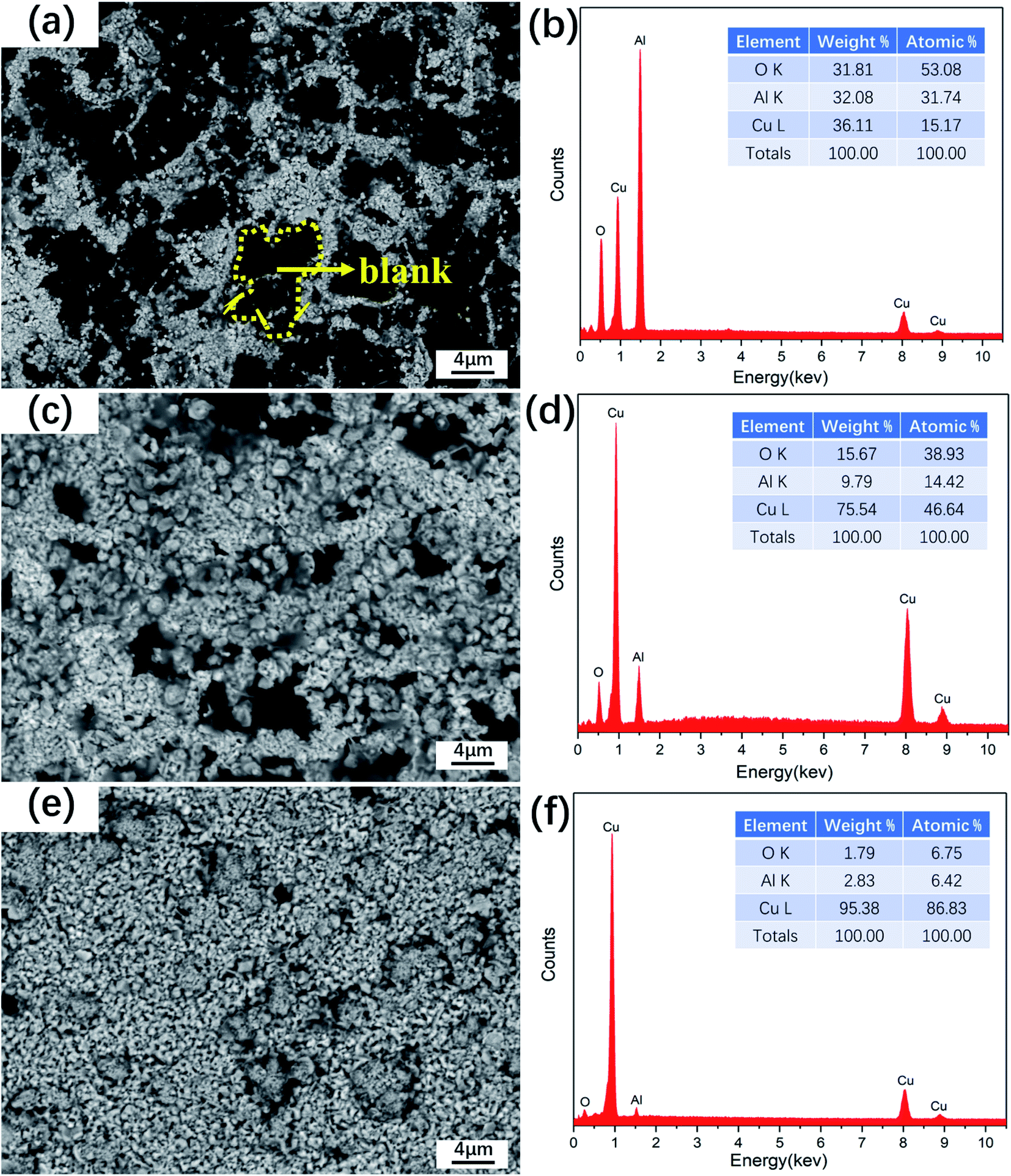 | ||
| Fig. 5 SEM image and EDS analysis of the copper layer deposited on Al2O3 substrate with different ECP times. (a and b) 15 min, (c and d) 35 min, (e and f) 60 min. | ||
As shown in Fig. 5c, when the reaction time is 35 minutes, it is in the rapid deposition stage, the deposition of copper particles is dense, and they have gradually become connected. Although there are “blanks”, the number is small and the distribution is narrow. When the electroless plating time reaches 60 minutes, as shown in Fig. 5e, the reaction reaches the deposition dynamic balance stage, the continuity of the plating layer is very good, and the deposited copper particles are particularly dense. Although there are some defects in the plating layer, the proportion is relatively small and completely acceptable. The main trend of the copper plating reaction on the surface of the substrate can also be seen from the energy spectrum in Fig. 5b, d and f. As the reaction time progresses, increasing amounts of copper deposits, and the signal from the plating layer becomes increasingly strong, while the signal from the substrate decreases steadily in strength. These results indicate that as the plating time increases, continuous growth of the copper layer can be achieved on Al2O3 ceramics.
Fig. 6e shows the variation of coating roughness with reaction time, combined with Fig. 6a–d, which shows the topography of the coating at different reaction times. The roughness changed little, and the surface quality was good. The topography was also highly intuitive in showing the good uniformity and low roughness of the coating.
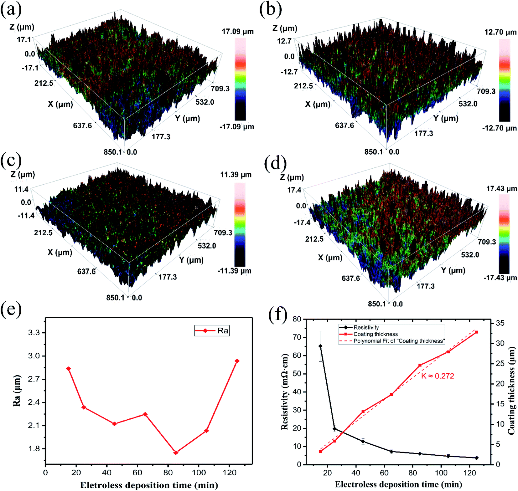 | ||
| Fig. 6 (a–d) The surface morphology of the coating at different reaction times: (a) 15 min, (b) 45 min, (c) 85 min, (d) 125 min; (e) roughness change diagram for different reaction times; (f) the resistivity change graph and coating thickness of different reaction time. | ||
Resistivity indicates the electrical properties of the coating and is a very important indicator of the quality of the coating. With the increase of the electroless plating reaction time, the resistivity of the plating layer steadily decreased; that is, the electrical conductivity gradually improved and finally tended to balance, as shown in Fig. 6f. In the first stage, the deposited copper was distributed in clusters, the copper layer on the surface was less and unevenly distributed, and there were few interconnections, which led to a high resistivity and an increase in the surface roughness. In the second stage, the thickness of the copper layer gradually increased, the copper layers in different areas began to connect to make up for the “blank” area, and the roughness gradually decreased, while the quality of the plating layer improved. At the same time, the resistivity dropped rapidly. When the reaction entered the third stage, the coating fully covered the substrate and was thicker, the resistivity gradually stabilized, and the conductivity was better. When the reaction time was too long, however, the roughness of the coating increased rapidly. Fig. 6f also indicates the relationship between the thickness of the coating layer over time. It provides a basis to control the thickness of the coating. These results indicate that the copper coating on the Al2O3 ceramic surface has better surface uniformity and less roughness and better electrical conductivity. This is of great significance to its welding performance and it can be applied to some microwave devices, such as ceramic filters, antennas, frequency selective surfaces, and other devices that have higher requirements for surface quality.
3.4. Performance of the coating
Fig. 7a shows the change in resistance of copper plating with and without anti-oxidation treatment when exposed to air to determine its stability and reliability. We found that with the increase of the exposure time in the air, the resistance of the copper layer without anti-oxidation treatment changed greatly, and the resistance value almost doubled. However, the resistance of the copper layer after the anti-oxidation treatment changed more gently and the range of change was small, which shows the good stability of the plating layer.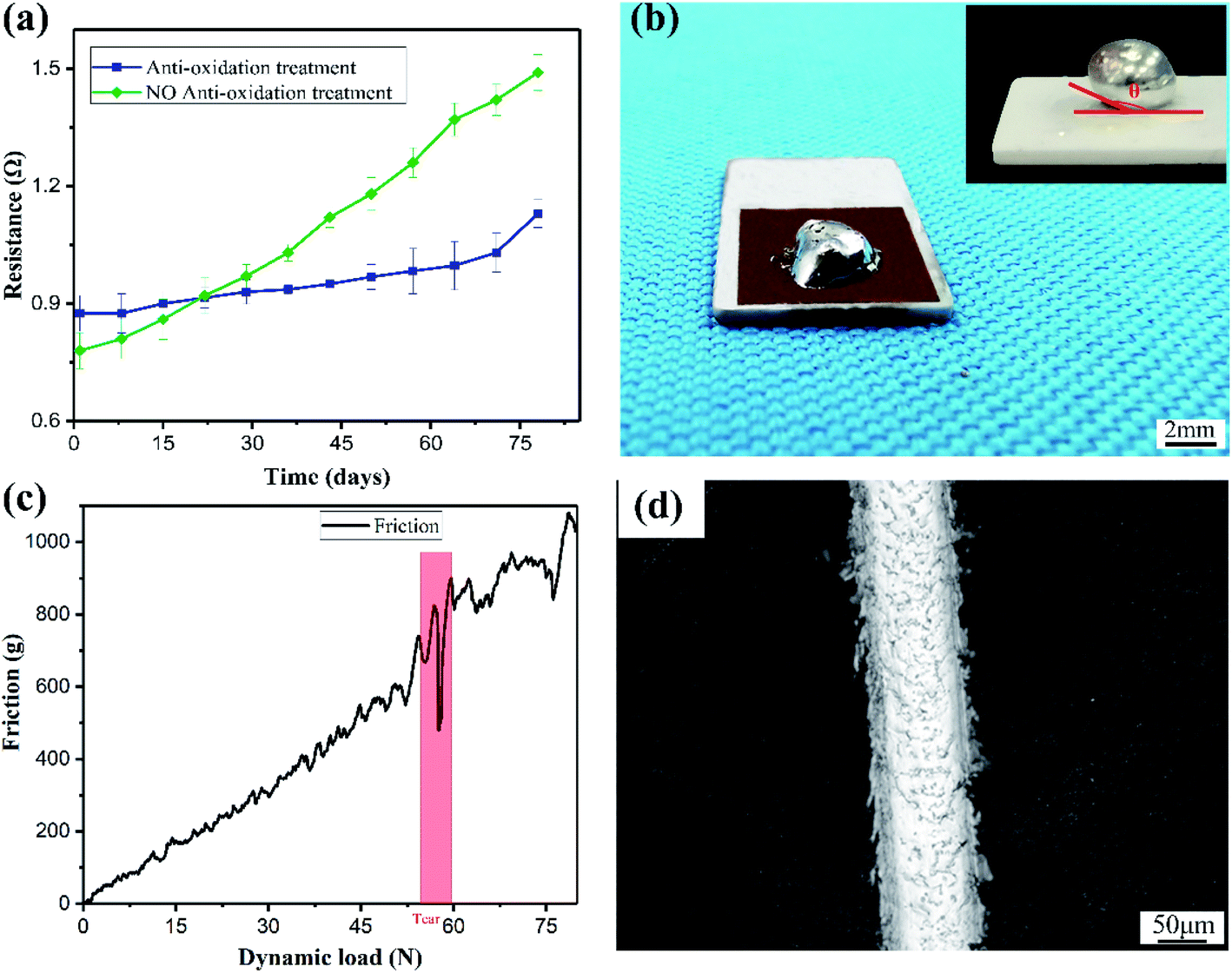 | ||
| Fig. 7 Performance of copper plating. (a) Resistance change of copper plating layer placed in the air, (b) solderability of copper plating layer, (c) cohesion of plating layer, (d) micrograph of scratch. | ||
Fig. 7c shows the combination of copper plating and ceramic substrate. The dynamic loading force was 80 N, the rate was 10 N min−1, and the final scratch length was 5 mm. The sudden change of the curve occurred in the interval of 55–60 N, which indicates that the substrate tore off from the plating. Although the curve fluctuated before tearing, it remained very stable overall, which also shows that the roughness of the coating was small and the uniformity of the coating good, which is very important for its practical application. Through the imprint of the scratch in Fig. 7d, we found that the coating on both sides of the scratch did not have obvious tearing off. This also shows the superior bonding performance of the copper coating and the ceramic substrate.
For the application of ceramic surface metallization, the welding performance of the coating also had to be considered. Fig. 7b shows that when the solder dropped on the square copper layer, the irregular shape was firmly welded to the copper layer. When the solder dropped on the ceramic, it took a spherical shape with a contact angle θ > 90°, which indicates that the soldering performance between the solder and the ceramic was extremely poor.
The comparison shows that the selective metallization of the ceramic surface can be used well in the circuit board, and compared with the traditional PCB material, no solder mask is required. The good weldability of the copper plating layer and the poor weldability of the ceramic provide the basis for the application of Fig. 8.
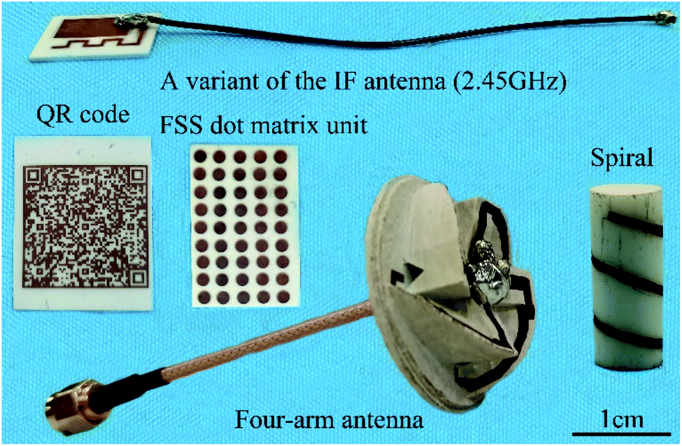 | ||
| Fig. 8 Some applications by LPA and ECP. | ||
The prototype in Fig. 8 was made by LPA and ECP, including the variant of classic IF antenna, a QR code with author information (you can scan it with a mobile phone), a dot matrix unit for frequency selection surfaces, a spiral around the cylinder, and a four-arm antenna. All these show the good application prospects of the combination of LPA and ECP on Al2O3 ceramics.
4. Conclusions
A complete process method for selective metallization of ceramic surfaces based on 3D printing is studied here. A self-developed DLP printer was used to prepare Al2O3 ceramic substrates, and a laser was used to selectively pre-treat the ceramic surface to prepare for the subsequent ECP. The resistance and thickness of the coating can be easily adjusted through the electroless plating process. The prepared copper layer has low resistivity, good stability, satisfactory solderability, and reliable bonding force, which are all important features for its application. This simple, low-cost, and effective method makes it possible to use ceramic substrates in the miniaturization of integrated circuits, antennas, filters, and other devices.Conflicts of interest
There are no conflicts to declare.Acknowledgements
This work is supported by National Key Research and Development Program (Grant No. 2018YFB1105400), Jiangsu Province Key Research and Development Program (Grant No. BE2017001-3 and BE2019002-1), Foundation of Key Laboratory of precision manufacturing technology of China Academy of Engineering Physics (Grant No. CAEP. ZT17001) and the Fund for Basic Strengthening Program in Technology Field (Grant No. 2019-JCJQ-JJ-342). The authors also extend their sincere thanks to those who contributed in instructions and experiments work.References
- H. Jha, T. Kikuchi, M. Sakairi and H. Takahashi, Electrochim. Acta, 2007, 52, 4724–4733 CrossRef CAS.
- R. K. Sharma, R. Kaneriya, S. Patel, A. Bindal and K. C. Pargaien, Microelectron. Eng., 2013, 108, 45–49 CrossRef CAS.
- A. Christensen and S. Graham, Appl. Therm. Eng., 2009, 29, 364–371 CrossRef CAS.
- C. Qian, A. M. Gheitaghy, J. J. Fan, H. Y. Tang, B. Sun, H. Y. Ye and G. Q. Zhang, IEEE Access, 2018, 6, 12868–12884 Search PubMed.
- A. Raveendran, M. T. Sebastian and S. Raman, J. Electron. Mater., 2019, 48, 2601–2634 CrossRef CAS.
- P. E. Koziol, A. J. Antonczak, P. Szymczyk, B. Stepak and K. M. Abramski, Appl. Surf. Sci., 2013, 287, 165–171 CrossRef CAS.
- A. V. Belyakov, I. G. Kuznetsova, R. Y. Kuftyrev, L. V. Pilavova and V. S. Seregin, Glass Ceram., 2012, 69, 270–273 CrossRef CAS.
- S. K. Lee, W. H. Tuan, Y. Y. Wu and S. J. Shih, J. Eur. Ceram. Soc., 2013, 33, 277–285 CrossRef CAS.
- J. A. Fernie, R. A. L. Drew and K. M. Knowles, Int. Mater. Rev., 2009, 54, 283–331 CrossRef CAS.
- Y. Y. Xu, X. J. Mao, J. T. Fan, X. K. Li, M. H. Feng, B. X. Jiang, F. Lei and L. Zhang, Ceram. Int., 2017, 43, 8839–8844 CrossRef CAS.
- S. Leo, C. Tallon, N. Stone and G. V. Franks, J. Am. Ceram. Soc., 2014, 97, 3013–3033 CrossRef CAS.
- M. Jabbari, R. Bulatova, A. I. Y. Tok, C. R. H. Bahl, E. Mitsoulis and J. H. Hattel, J. Mater. Sci. Eng. B, 2016, 212, 39–61 CrossRef CAS.
- E. MacDonald and R. Wicker, Science, 2016, 353, 8 CrossRef.
- S. Y. Ma, L. Liu, V. Bromberg and T. J. Singler, ACS Appl. Mater. Interfaces, 2014, 6, 19494–19498 CrossRef CAS.
- H. Minemawari, T. Yamada, H. Matsui, J. Tsutsumi, S. Haas, R. Chiba, R. Kumai and T. Hasegawa, Nature, 2011, 475, 364–367 CrossRef CAS.
- S. S. Akhtar, L. T. Kareem, A. F. M. Arif, M. U. Siddiqui and A. S. Hakeem, Ceram. Int., 2017, 43, 5236–5246 CrossRef CAS.
- M. Uysal, R. Karslioglu, A. Alp and H. Akbulut, Ceram. Int., 2013, 39, 5485–5493 CrossRef CAS.
- H. F. Ma, Z. B. Liu, L. Wu, Y. H. Wang and X. X. Wang, Thin Solid Films, 2011, 519, 7860–7863 CrossRef CAS.
- G. B. Lin, J. H. Huang and H. Zhang, J. Mater. Process. Technol., 2007, 189, 256–261 CrossRef CAS.
- J. M. Fernandez, R. Asthana, M. Singh and F. M. Valera, Ceram. Int., 2016, 42, 5447–5454 CrossRef CAS.
- X. Wei, H. X. Xu, J. Zhan, H. Zhang, Y. Cao, S. Cui and W. M. Tang, Ceram. Int., 2018, 44, 18935–18941 CrossRef CAS.
- H. Zhao, L. Hou, J. X. Wu and Y. X. Lu, J. Mater. Chem. C, 2016, 4, 7156–7164 RSC.
- S. Shao-Ping and D. Wei-Ping, J. Electrochem. Soc., 2014, 161, D579–D585 CrossRef.
- A. A. Zaman and C. S. Dutcher, J. Am. Ceram. Soc., 2006, 89, 422–430 CrossRef CAS.
- H. D. Wu, Y. L. Cheng, W. Liu, R. X. He, M. P. Zhou, S. H. Wu, X. Song and Y. Chen, Ceram. Int., 2016, 42, 17290–17294 CrossRef CAS.
- W. H. Tuan and S. K. Lee, J. Eur. Ceram. Soc., 2014, 34, 4117–4130 CrossRef CAS.
- G. A. Shafeev, Appl. Phys. A: Mater. Sci. Process., 1998, 67, 303–311 CrossRef CAS.
- E. Ermantraut, H. Muller, W. Eberhardt, P. Ninz, F. Kern, R. Gadow and A. Zimmermann, IEEE Trans. Compon., Packag., Manuf. Technol., 2019, 9, 138–145 CAS.
- G. A. Shafeev, Adv. Mater. Opt. Electron., 1993, 2, 183–189 CrossRef CAS.
- M. J. DeSilva, A. J. Pedraza and D. H. Lowndes, J. Mater. Res., 1994, 9, 1019–1027 CrossRef CAS.
- R. Lahoz, G. F. de la Fuente, J. M. Pedra and J. B. Carda, Int. J. Appl. Ceram. Technol., 2011, 8, 1208–1217 CrossRef CAS.
- D. Bäuerle, Laser Processing and Chemistry, Springer, Berlin, Heidelberg, 4th edn, 2011 Search PubMed.
- L. C. Tshabalala and S. Pityana, Surf. Coat. Technol., 2016, 289, 52–60 CrossRef CAS.
- C. Dupas-Bruzek, L. D. Laude, F. Langenhorst and K. Kolev, J. Appl. Phys., 2003, 93, 4489–4496 CrossRef CAS.
Footnote |
| † These authors contributed equally. |
| This journal is © The Royal Society of Chemistry 2020 |