DOI:
10.1039/D0RA08360G
(Paper)
RSC Adv., 2020,
10, 42157-42163
Controlled synthesis of few-layer SnSe2 by chemical vapor deposition†
Received
30th September 2020
, Accepted 13th November 2020
First published on 19th November 2020
Abstract
Few-layer SnSe2 has intrinsic low thermal conductivity and unique phase transition from amorphous to crystalline state under laser irradiation. It has been extensively used in the fields of thermoelectric conversion and information storage. However, the traditional precursors like tin oxide and organic compounds have either high melting points or complex compositions, and the improper deposition temperature of the substrate may lead to mixed products, which impedes controllable synthesis of high-quality few-layer SnSe2. Here, we propose a chemical vapor deposition (CVD) method, in which the precursor evaporation and deposition have been controlled via the adjustment of precursors/substrate positions, which effectively avoided mixed product growth, thus achieving the growth of high-quality few-layer SnSe2. The calculated first-order temperature coefficient of the A1g module is −0.01549 cm−1 K−1, which is superior to other two-dimensional (2D) materials. Meanwhile, two exciton emissions from few-layer SnSe2 have been found, for which the higher energy one (1.74 eV) has been assigned to near-band-gap emission, while the lower one (1.61 eV) may have roots in the surface state of SnSe2. The few-layer SnSe2 also exhibits large exciton binding energies (0.195 and 0.177 eV), which are greater than those of common semiconductors and may contribute to stability of excitons, showing broad application prospects in the field of optoelectronics.
1. Introduction
As an important member of two-dimensional (2D) layered materials, the group-IV metal chalcogenides (GIVMCs) have advantages like abundant earth reserves, environmentally-friendly features and low cost.1–3 The GIVMC semiconductors have diverse electron band structures, and their band gaps correspond to a photoresponse spectrum ranging from ultraviolet to mid-infrared.4–7 Unlike element of other group, the metal atoms of GIVMCs semiconductors have +4 or +2 valence states, both states can coordinate with chalcogens atoms to form 2D materials. Especially for the metal element Sn, the formed chalcogenide SnSe2 is a n-type indirect semiconductor with a hexagonal crystal structure similar to CdI2, while the elements in the same group mostly form p-type indirect semiconductor with orthorhombic crystal structure.8 SnSe2 is a promising material in the field of thermoelectricity, which has relatively lower lattice thermal conductivity compared to graphene.9 Meanwhile, the quick and reversible transformation of SnSe2 from crystal to amorphous under laser irradiation make it a typical phase change materials which can be used for information storage.10,11 What's more, SnSe2 is also a nova material in the field of photoelectricity because of its high responsivity (1.1 × 10³ A W−1), high on/off ratio and fast response rate.12 Despite the excellent properties mentioned above, there still exist challenges for SnSe2 synthesis techniques.9,13,14 On one hand it is limited due to the precursor selection, general precursors like tin oxides have relatively high melting points,1 while other precursors like organic compound [SnCl4{nBuSe(CH2)nSenBu}] made by artificial cumbersome steps are extremely sensitive to moisture and oxygen,15 thus the evaporation of precursors is uncontrolled and affects the morphology of the SnSe2 product. On the other hand, due to the improper deposition temperature of substrate, the obtained SnSe2 product is usually mixed with a large number of impure phase (SnSe or Se).12,16,17 Thus till today, most of the current researches can only product multilayers or bulk SnSe2.18 However, compared to bulk material, properties of single crystal in 2D few layers material can effectively avoid the influence of grain boundary.19 Additionally, there are also researches demonstrating that few layers samples have higher carrier mobility than their bulk counterparts.20,21 Therefore, the synthesis of few-layer SnSe2 samples are important for further properties and applications exploration. At the present, only a few studies have achieved the preparation of few-layer SnSe2. In these studies, Athanasios and co-workers22 fabricated few-layer SnSe2 by molecular beam epitaxy (MBE) technique. Liu and co-workers23 have synthesized single crystal of SnSe2 by chemical vapor transport (CVT) method, then obtained few-layer SnSe2 via mechanically exfoliated method. Zhai and co-workers12 for the first time obtained high quality ultrathin SnSe2 (with a thickness of 1.5 nm, corresponds to only two atomic layers) by chemical vapor deposition (CVD) method. However, problems like high instrument costs, low yield, uncontrollable size are still existing.
To address the issues mentioned above, based on the research of reaction thermodynamics, a CVD synthesis method with SnI2 and Se as precursors has been proposed, in which the evaporation of precursors has been controlled via the sources position, which kept the vapor pressures consistent at the growth locations, while the deposition temperature has been controlled via the substrate position, which effectively avoided impure phase growth, thus achieving the growth of high-quality few-layer SnSe2. Atomic force microscopy (AFM), Raman, photoluminescence (PL) and X-ray Photoelectron Spectroscopy (XPS) characterization reveal that the as-synthesized few-layer SnSe2 (with a thickness of 1.34 nm) are of high quality with an indirect bandgap ≈1.74 eV, while subsequent variable temperature (77–298 K) Raman and PL measurements provide SnSe2 lattice vibration and exciton emission information for further fundamental research and potential applications exploitation in thermoelectric and optoelectronics field.
2. Experimental section
2.1 Fabrication of SnSe2
The SnSe2 crystals were synthesized on mica substrates via atmospheric pressure CVD method, with the CVD procedures carried out using a Mini-Mite™ tube furnace, which is purchased from Lindberg/Blue M. Before the synthesis, high purity Se powder (99.5%, about 0.02 g) and SnI2 powder (99.999%, about 0.01 g) were placed in two separate quartz boats, and placed 15 cm and 14 cm upstream from the center heating zone respectively in a quartz tube. All the chemicals were purchased from Alfa and used as received without further purification. To provide the growth locations for the synthesis product, the substrates were placed 10, 12, and 14 cm downstream from the center heating zone, respectively. Ar (20 sccm) and H2 (5 sccm) were used as carrier gas and sent into the furnace for the whole synthesis process. During the synthesis, the furnace was firstly heated to 915 K in 15 min, and naturally cooled to room temperature after 10 min system stabilization.
2.2 Characterization methods
The optical images were taken with Olympus BX51 optical microscopy. The AFM images were taken with Bruker MultiMode 8 atomic force microscope. The XPS spectra were collected with ESCALAB 250Xi X-ray photoelectron spectroscopy. The Raman and PL spectra were collected with Witec alpha 300 confocal Raman spectroscopy.
3. Results and discussion
High quality few-layer SnSe2 were synthesized by CVD method, Fig. 1(a) illustrates the CVD process for few-layer SnSe2 fabrication. During the growth process, we used SnI2 and Se powders as precursors, and mica as substrate. Unlike most tin oxides with high melting points or organic compounds [SnCl4{nBuSe(CH2)nSenBu}] with complex composition, SnI2 has a relatively low evaporation temperature (590.15 K) and a simple chemical composition. It can provide more uniform and stable growth conditions for the CVD process.12 Mica is a 2D layered material without hanging bond on the surface, the migration barrier of the adsorbed atoms on mica surface is much smaller than that on silicon substrate, which permits rapid migration of the adsorbed atoms on the mica surface, thus contributes to a better CVD growth of few layers 2D materials. In contrast with mica substrate, it is easily to grow thick SnSe2 flakes on silicon substrate due to lots of dangling bonds existing on its surface (as shown in Fig. S1†). The detailed experimental procedure is described in the Experiment section. Growth mechanism with two steps was proposed to describe the SnSe2 growth process. The first step is the evaporation and diffusion of precursor sources. According to the results of thermodynamic calculations, the simulation results of SnI2 and Se vapor pressures as a function of temperature are showed in Fig. 1(c) and (d), more details are showed in ESI.† Combining with the actual measured furnace temperature results (Fig. 1(b)), Se powder and SnI2 powder were put in two separated quartz boats, and placed 15 cm and 14 cm upstream from the center heating zone, corresponding to the 540 K and 625 K respectively. After the transport of precursors vapor to the substrate position by carrier gas, atoms released by precursor sources occurred to adsorb and desorb on the substrate, the adsorbed Se and Sn atoms will migrate and react with each other, thus leading to nucleation and growth of SnSe2. When the substrate was located at different positions, different number of adsorbed active atoms would desorb and evaporate into carrier gas.24,25 The rate of atoms migrations J can be described by eqn (1)where ∇C is the atoms concentration gradient, D is the atoms migration coefficient, which is related to the nature of the adsorbent, and the fact that relative atomic mass of Sn is larger than Se results in DSn < DSe at the same temperature. Noticing that the atoms migration coefficient D is also proportional to e−Em/kT (where Em is migration barrier energy; k is Boltzmann constant; T is temperature), it's easy to understand that the migration rate is reduced with the decrease of substrate temperature.26 According to our experiment results, when the mica substrate was located at 12 cm downstream from the center heating zone, corresponding to the temperature of 750 K, the temperature permitted relatively suitable migration rate of the adsorbed atoms on the mica surface, and the SnSe2 growth temperature was ensured synchronously, which benefitted few-layer SnSe2 growth (Fig. S2(b)†). When the mica substrate was placed at 10 cm downstream from the center heating zone, corresponding to relatively higher temperature (820 K), Se atoms would react more vigorously with Sn atoms under fast atoms migration rate, meanwhile there were part of adsorbed Se atoms on substrate which would desorb into the carrier gas due to the high temperature.25 Additionally, as the growth temperature of SnSe is higher than SnSe2, it's easier to fabricate SnSe under a relatively high temperature. Therefore, thick SnSe with square shaped were fabricated on mica substrate (Fig. S2(a)†) at this occasion. In contrast, when the substrate was placed at 14 cm downstream from the center heating zone, which corresponds to lower temperature (625 K), the growth rate of the sample and the nucleation density decreased due to the slow atoms migration, only a few samples were collected on mica, as shown in Fig. S2(c).† Based on the thermodynamics calculation and prediction, controllable few-layer SnSe2 synthesis has been achieved.
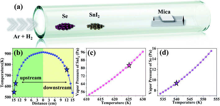 |
| | Fig. 1 Synthesis of SnSe2 by chemical vapor deposition method. (a) Schematic illustration of the CVD process for the synthesis of the SnSe2, where Se and SnI2 powder were used as the precursors. (b) Temperature profile of the furnace. (The heating zone of furnace was set to 915 K. The star marks from left to light represent Se, SnI2 and optimal mica locations, respectively. The distance of “0” represents the heating center of furnace.) (c) Vapor pressure dependence of SnI2 with temperature. (The star mark corresponds to the vapor pressure at 625 K.) (d) Vapor pressure dependence of Se with temperature. (The star mark corresponds to the vapor pressure at 540 K.) | |
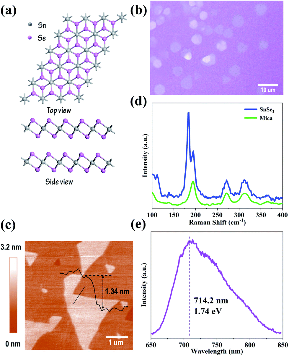
Structural model of SnSe2 is showed in Fig. 2(a), SnSe2 presents a hexagonal crystal structure governed by van der Waals interactions between the layers, each layer consists of “Se–Sn–Se” three atomic planes with internal covalent bonding. Fig. 2(b) shows optical image of the SnSe2 synthesized on mica substrate, showing their hexagon shape with lateral dimensions about 10 μm. AFM image of few-layer SnSe2 is showed in Fig. 2(c), which reveals the sample thickness is ∼1.34 nm, corresponding to two atomic layers SnSe2. Raman spectroscopy was performed to provide information about the quality of as-prepared few-layer SnSe2, and the corresponding result is shown in Fig. 2(d). Apparently, except mica peaks at 194 cm−1, 271 cm−1, 313 cm−1, there are two peaks located at 115 cm−1 and 184 cm−1, corresponding to Eg mode and A1g mode, which are caused by the in-plane and out-plane vibrations of the Se atoms, respectively.23 The intensity of Eg mode is significantly weak due to few scattering centers existing in few-layer SnSe2.12,27 Raman mapping of A1g mode shows the uniformity of the sample (Fig. S3(c)†), and the PL spectrum shows a peak centered at 714.2 nm (Fig. 2(e)), corresponding to a bandgap of 1.74 eV. All results above confirm that high crystalline quality few-layer SnSe2 has been synthesized via the proposed CVD method in which the thermodynamics parameters have been precisely controlled.
 |
| | Fig. 2 (a) Structural model of SnSe2. (b) Optical image of the SnSe2 synthesized on mica. (c) AFM image of few-layer SnSe2, the height profile shows a thickness of 1.34 nm (inset). (d) Raman spectra of SnSe2 at room temperature. (e) PL spectra of SnSe2 at room temperature. | |
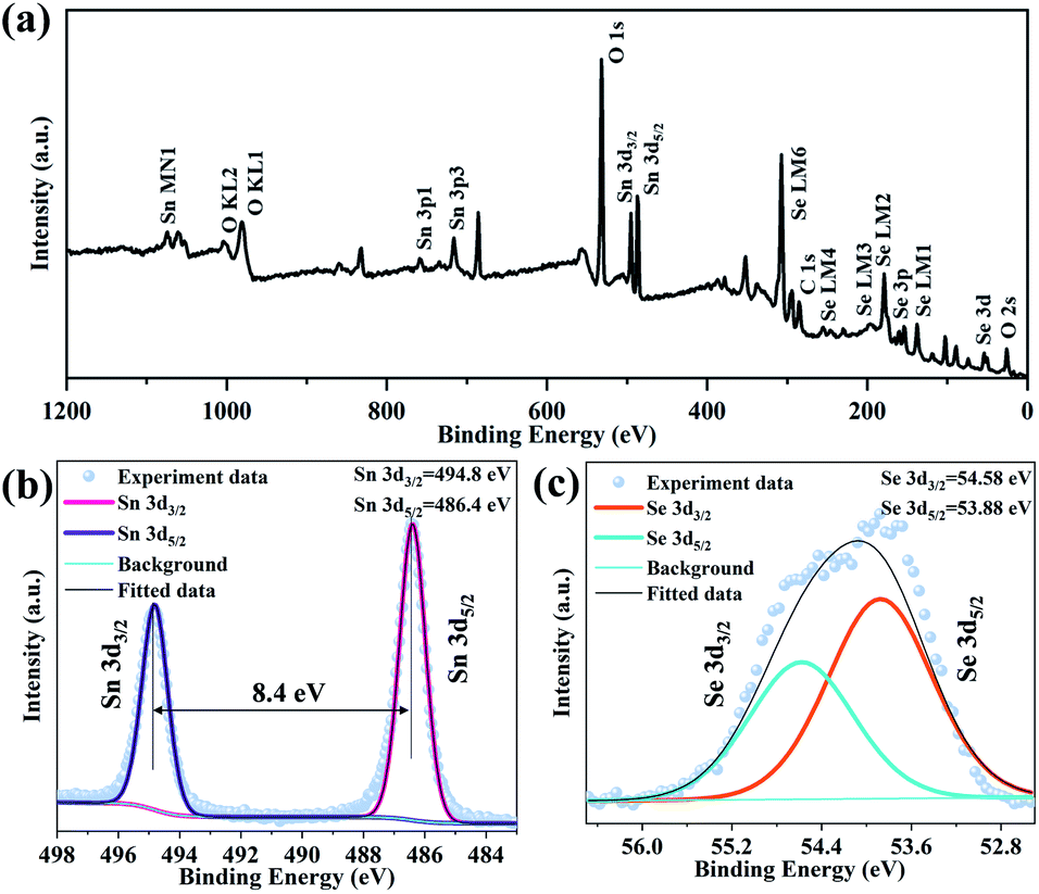
With the purpose of investigating the elemental composition and stoichiometry of the as grown SnSe2 on mica substrates, XPS was used. The binding energy is referenced to an adventitious C 1s peak at 284.6 eV. The typical XPS survey of SnSe2 is showed in Fig. 3(a), in which the peaks of Sn 3d, Se 3d and C 1s were identified respectively. The peak of O 1s is found because of the mica substrate. Then XPS spectra of Sn 3d and Se 3d were furtherly performed. The energy for Sn 3d3/2 and Sn 3d5/2 (Fig. 3(b)) are located at 494.8 eV and 486.4 eV, respectively. According to previous studies,28 the distance between these two peaks is 8.4 eV, revealing that the valence of Sn is +4. The spectra of the constituent element Se 3d is showed in Fig. 3(c), which splits into two states Se 3d3/2 and Se 3d5/2 through the peak fitting, relating to the binding energy of 54.58 eV and 53.88 eV respectively. Based on the analysis above, it also proved there is no presence of other oxidation states. The synthesis of high quality SnSe2 on mica substrates by CVD method has been confirmed.
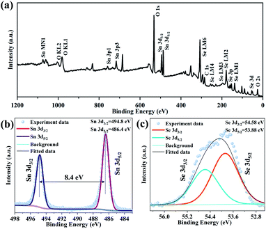 |
| | Fig. 3 XPS spectra of SnSe2 for typical survey (a), Sn 3d (b) and Se 3d (c), respectively. No presence of other oxidation states is realized. | |
Better heat dissipation may be one of the biggest challenges in electronic devices, as the performance and service life of the device are greatly affected by the self-heating effect.29,30 For this problem, it is important to investigate thermal property of materials.13
Raman spectroscopy can be used to characterize the lattice vibrations of materials rapidly and non-destructively, and provide information of lattice thermal property. Hence, lattice vibrations of few-layer SnSe2 were brought to research by temperature-dependent Raman test. There are several reasons for the temperature dependence of Raman modes position, such as electron–phonon, anharmonic phonon–phonon interactions and thermal expansion.29–31 SnSe2 is a 2D layered material, its interlayer van der Waals interaction tends to lead lower interfacial thermal conductivity. A1g mode corresponding to the out-of-plane vibration mode, this interlayer vibration is sensitive to temperature, and largely contributes to the total lattice thermal conductivity, so that the temperature dependence of A1g mode was investigated. In Fig. 4(a), we present Raman spectra of few-layer SnSe2 at temperature ranging from 77 K to 298 K. With temperature increase, A1g mode showed red shift, and the peak intensity increased, showing the general thermal effect of semiconductor. The Fig. 4(b) shows the typical plot of A1g mode positions as a function of temperature for few-layer SnSe2, which behaves linear relation from 77 K to 298 K. The Lorentzian fitting eqn (2) was used for calculating temperature coefficients (χ).32,33
where
ω0 is the A
1g position for temperature close to 0 K and
χ is the first-order temperature coefficient of A
1g mode. This equation is widely used for describing temperature dependence of Raman shifts for nanomaterials. The position of SnSe
2 A
1g mode decreased by ∼3.4 cm
−1 when the temperature increased from 77 K to 298 K, thus the calculated first order temperature coefficient
χ of A
1g is −0.01549 cm
−1 K
−1, this result is consistent with the literature,
32 which is superior to many other 2D materials. As the change in the A
1g mode is mostly due to the thermal expansion and volume contribution, based on its relatively high temperature coefficients result for A
1g modes, SnSe
2 can be used for monitoring local temperature in electronic operating device.
33
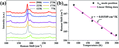 |
| | Fig. 4 Raman spectra of the (a) SnSe2 measured in the temperature range between 77 K and 298 K. (b) Temperature dependence of SnSe2 A1g mode position. | |
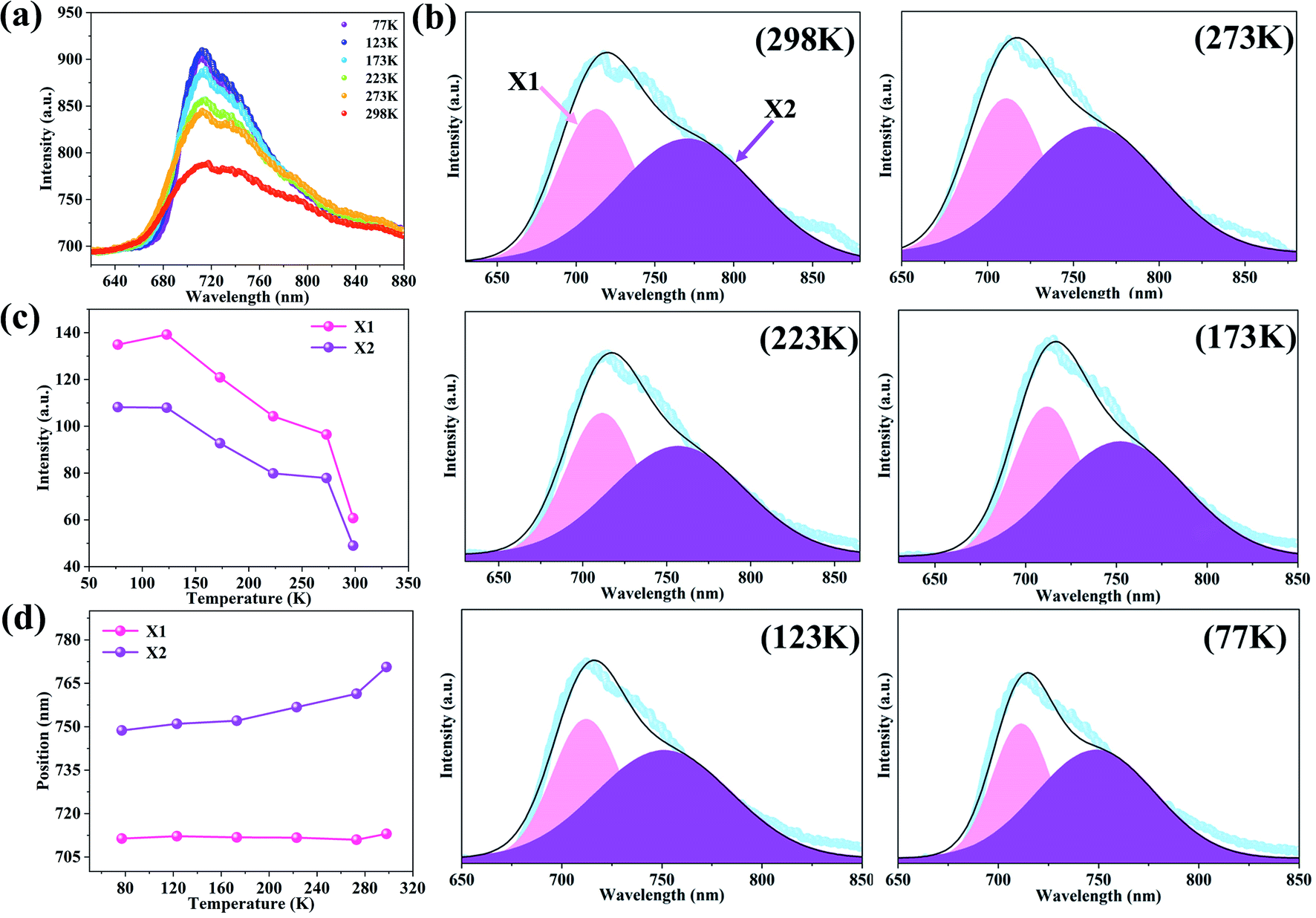
In the process of photoelectric conversion, the electrons are excited into the conduction band and the holes with positively charged are left in the valence band, the electrons and holes will form a bound state due to the strong coulomb interaction, which is called an exciton. In the semiconductor electronic devices, the existence of excitons plays a central role. The effective mass theory of 2D excitons has predicted that exciton binding energy of two layers SnSe2 is 0.229 eV.20 However, this value hasn't been experimentally verified. Therefore, the temperature-dependent PL measurements on the same SnSe2 was carried out to investigate its exciton binding energy. When the temperature increases from 77 K to 298 K, the PL intensity are generally weakened (Fig. 5(a)). There are some reasons for the weak PL intensity, one is that the SnSe2 is a natural indirect semiconductor, the extremes of the conduction band and valence band correspond to different wave vectors k, which means the transition between bands is an indirect one, thus during the transition process, in addition to emitting photons, phonons are also involved, which consume a part of energy. Beyond that, unlike d electrons of Mo, the element Sn has outer p electrons which are involved in the structural bonding, leading to very weak luminous intensity.13,34 When fitted by Gaussian functions, the temperature-dependent SnSe2 PL peak can be deconvoluted with X1 and X2 peaks (Fig. 5(b)). Not only the overall PL intensity but also the intensities of X1 and X2 peaks were weakened with the temperature increasing, as shown in Fig. 5(c). It is attributed to the thermally activated nonradiative recombination due to the increased interactions.35 That is, when the thermal motion of phonons is enhanced with the temperature rising, the nonradiative process will consume more photogenerated carriers, resulting in the weakened PL intensity. The temperature dependence of the PL intensity can be expressed by eqn (3),36
| |
I(T) = I0/(1 + A![[thin space (1/6-em)]](https://www.rsc.org/images/entities/char_2009.gif) exp[−EB/kBT]) exp[−EB/kBT])
| (3) |
where
I0 is the PL intensity at 0 K,
A is the fitting parameter,
EB is the exciton binding energy, and
kB is the Boltzmann constant. From the fitting curves in Fig. S4(a) and (b),
† the exciton binding energies of X1 and X2 peaks are calculated to be 0.195 and 0.177 eV respectively, which are greater than those of common semiconductors, and approximately equal to the calculated theoretical value 0.229 eV. The large exciton binding energy is helpful for stabilizing an exciton in a nanosystem.
37 In the
Fig. 5(d), the PL positions of X1 increased ∼2.02 nm when the temperature increased from 77 K to 298 K, which showed a redshift of energy ∼0.005 eV. The X1 peak is attributed to the near-band-gap emission,
38 which is speculated to be associated with phonons interaction. However, as the phonons interaction is greatly weakened at low temperature, it can't reflect the bandgap change, resulting in no obvious change for X1 peak position. Meanwhile, for the PL position of X2 peak, with the temperature increase, this position increased from 748.7 nm to 770.6 nm, corresponding to an energy decrease from 1.66 eV to 1.61 eV. This phenomenon may result from the surface defect state of SnSe
2.
38,39 The dynamics of exciton and scattering mechanism are still not clearly, which call for further investigations.
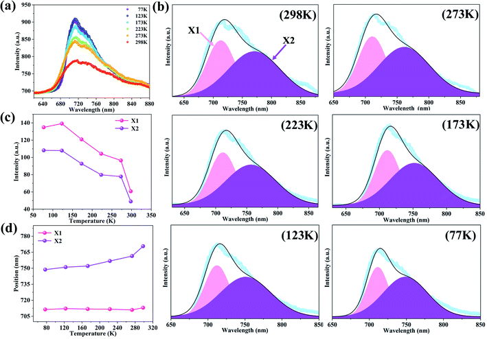 |
| | Fig. 5 PL spectra of the (a) SnSe2 measured in temperature range from 77 K to 298 K. (b) Temperature dependent PL spectra fitted by the Gaussian distribution. (c) The intensity of X1 and X2 varying with temperature. (d) The position of X1 and X2 varying with temperature. | |
4. Conclusions
In conclusion, we obtained few-layer SnSe2 by CVD method with SnI2 and Se as precursors, achieving controllable precursors evaporation and avoid mixed products via adjust the positions of precursors/substrate. The temperature dependent Raman and PL tests of the products were carried out subsequently, and the first-order temperature coefficient of A1g module was measured to be −0.01549 cm−1 K−1, which is superior to other 2D materials, showing great potential for application in 2D electronic device. Meanwhile, we found two exciton emissions from few-layer SnSe2. The higher energy emission (1.74 eV) may be referred to near-band-gap emission, while the lower one (1.61 eV) may be affected by the surface state of SnSe2. The exciton binding energy of X1 and X2 are about 0.195 and 0.177 eV respectively, which may signify a relatively good stability against thermal dissociation of excitons. The few-layer SnSe2 have a promising prospect for future thermoelectric and optoelectronics field. What's more, this synthetic method by precisely controlling the thermodynamics parameters can be extended to other 2D materials growth.
Conflicts of interest
There are no conflicts to declare.
Acknowledgements
This work was financially supported by the National Science Foundation of China (NSFC, Grant No. 61922005 and U1930105), the Equipment Pre-research Project of China Electronics Technology Group Corporation (CETC) (Grant No. 6141B08110104), the General Program of Science and Technology Development Project of Beijing Municipal Education Commission (Grant No. KM202010005005) and the Doctoral Scientific Research Foundation of BJUT (Grant No. 048000514120549).
Notes and references
- J. J. Wu, Z. L. Hu, Z. H. Jin, S. D. Lei, H. Guo, K. Chatterjee, J. Zhang, Y. C. Yang, B. Li, Y. Liu, J. W. Lai, R. Vajtai, B. Yakobson, M. Tang, J. Lou and P. M. Ajayan, Adv. Mater. Interfaces, 2016, 3, 1600383 CrossRef.
- S. L. Zhao, H. Wang, Y. Zhou, L. Liao, Y. Jiang, X. Yang, G. C. Chen, M. Lin, Y. Wang, H. L. Peng and Z. F. Liu, Nano Res., 2015, 8, 288–295 CrossRef CAS.
- G. P. Li, G. Q. Ding and G. Y. Gao, J. Phys.: Condens. Matter, 2017, 29, 015001 CrossRef.
- X. Zhou, L. Gan, Q. Zhang, X. Xiong, H. Q. Li, Z. Q. Zhong, J. B. Han and T. Y. Zhai, J. Mater. Chem. C, 2016, 4, 2111–2116 RSC.
- Y. S. Yang, S. C. Liu, X. Wang, Z. B. Li, Y. Zhang, G. M. Zhang, D. J. Xue and J. S. Hu, Adv. Funct. Mater., 2019, 29, 1900411 CrossRef.
- K. Chang, J. W. Liu, H. C. Lin, N. Wang, K. Zhao, A. M. Zhang, F. Jin, Y. Zhong, X. P. Hu, W. H. Duan, Q. M. Zhang, L. Fu, Q. K. Xue, X. Chen and S.-H. Ji, Science, 2016, 353, 274–278 CrossRef CAS.
- G. L. Ye, Y. J. Gong, S. D. Lei, Y. M. He, B. Li, X. Zhang, Z. H. Jin, L. L. Dong, J. Lou, R. Vajtai, W. Zhou and P. M. Ajayan, Nano Res., 2017, 10, 2386–2394 CrossRef CAS.
- M. I. Serna, S. M. N. Hasan, S. N. L. E. Bouanani, S. Moreno, H. Choi, H. N. Alshareef, M. M. Jolandan and M. A. Q. Lopez, Adv. Mater. Interfaces, 2018, 5, 1800128 CrossRef.
- A. Shafique, A. Samad and Y. H. Shin, Phys. Chem. Chem. Phys., 2017, 19, 20677 RSC.
- M. Micoulaut, W. Wełnic and M. Wuttig, Phys. Rev. B: Condens. Matter Mater. Phys., 2008, 78, 224209 CrossRef.
- X. Zhou, Q. Zhang, L. Gan, H. Q. Li, J. Xiong and T. Zhai, Adv. Sci., 2016, 3, 1600177 CrossRef.
- X. Zhou, L. Gan, W. M. Tian, Q. Zhang, S. Y. Jin, H. Q. Li, Y. Bando, D. Golberg and T. Y. Zhai, Adv. Mater., 2015, 27, 8035–8041 CrossRef CAS.
- W. Zhou, Z. H. Yu, H. Song, R. Y. Fang, Z. T. Wu, L. Li, Z. H. Ni, W. Ren, L. Wang and S. C. Ruan, Phys. Rev. B, 2017, 96, 035401 CrossRef.
- J. C. Liu, M. Z. Zhong, X. Liu, G. Z. Sun, P. Chen, Z. W. Zhang, J. Li, H. F. Ma, B. Zhao, R. X. Wu, W. Q. Dang, X. D. Yang, C. Dai, X. W. Tang, C. Fan, Z. J. Chen, L. L. Miao, X. Q. Liu, Y. Liu, B. Li and X. D. Duan, Nanotechnology, 2018, 29, 474002 CrossRef.
- C. H. de Groot, C. Gurnani, A. L. Hector, R. Huang and M. Jura, Chem. Mater., 2012, 24, 4442–4449 CrossRef CAS.
- P. A. Fernandes, M. G. Sousa, P. M. P. Salomé, J. P. Leitão and A. F. da Cunha, CrystEngComm, 2013, 15, 10278–10286 RSC.
- N. D. Boscher, C. J. Carmalt, R. G. Palgrave and I. P. Parkin, Thin Solid Films, 2008, 516, 4750–4757 CrossRef CAS.
- Y. Su, M. A. Ebrish, E. J. Olson and S. J. Koester, Appl. Phys. Lett., 2013, 103, 263104 CrossRef.
- D. Rhodes, S. Hoon Chae, R. R. Palau and J. Hone, Nat. Mater., 2019, 18, 541–549 CrossRef CAS.
- J. M. Gonzalez and I. I. Oleynik, Phys. Rev. B, 2016, 94, 125443 CrossRef.
- M. S. Long, P. Wang, H. H. Fang and W. D. Hu, Adv. Funct. Mater., 2018, 29, 1803807 CrossRef.
- K. E. Aretouli, D. Tsoutsou, P. Tsipas, J. M. Velasco, S. A. Giamini, N. Kelaidis, V. Psycharis and A. Dimoulas, ACS Appl. Mater. Interfaces, 2016, 8, 23222–23229 CrossRef CAS.
- P. Yu, X. C. Yu, W. L. Lu, H. Lin, L. F. Sun, K. Z. Du, F. C. Liu, W. Fu, Q. S. Zeng, Z. X. Shen, C. H. Jin, Q. J. Wang and Z. Liu, Adv. Funct. Mater., 2016, 26, 137–145 CrossRef CAS.
- Z. G. Wang and F. Pang, Chem. Phys. Lett., 2018, 702, 90–95 CrossRef CAS.
- Y. Huang, K. Xu, Z. X. Wang, T. A. Shifa, Q. S. Wang, F. Wang, C. Jiang and J. He, Nanoscale, 2015, 7, 17375–17380 RSC.
- L. Huang, Y. F. Yu, C. Li and L. Y. Cao, J. Phys. Chem. C, 2013, 117, 6469–6475 CrossRef CAS.
- P. A. Hu, Z. Z. Wen, L. F. Wang, P. H. Tan and K. Xiao, ACS Nano, 2012, 6, 5988–5994 CrossRef CAS.
- E. P. Mukhokosi, S. B. Krupanidhi and K. K. Nanda, Sci. Rep., 2017, 7, 15215 CrossRef.
- A. S. Pawbake, M. B. Erande, S. R. Jadkar and D. J. Late, RSC Adv., 2016, 6, 76551–76555 RSC.
- X. K. Liu, Z. L. Wen, L. Min, Y. F. Peng, X. B. Xiong, Y. M. Lu, J. P. Ao, J. P. Fang, W. He, K. L. Li, J. Wu, W. Mao, U. Younis and V. D. Botcha, J. Alloys Compd., 2019, 783, 226–231 CrossRef CAS.
- A. Taube, A. Łapińska, J. Judek and M. Zdrojek, Appl. Phys. Lett., 2015, 107, 013105 CrossRef.
- A. S. Pawbake, A. Date, S. R. Jadkar and D. J. Late, ChemistrySelect, 2016, 1, 5380–5387 CrossRef CAS.
- A. S. Pawbake, M. S. Pawar, S. R. Jadkar and D. J. Late, Nanoscale, 2016, 8, 3008–3018 RSC.
- C. Julien, M. Eddrief, I. Samaras and M. Balkanski, Mater. Sci. Eng., B, 1992, 15, 70–72 CrossRef.
- Y. F. Chen, W. Wen, Y. M. Zhu, N. N. Mao, Q. L. Feng, M. Zhang, H. P. Hsu, J. Zhang, Y. S. Huang and L. M. Xie, Nanotechnology, 2016, 27, 445705 CrossRef.
- X. Zhou, J. T. Lü, N. Zhou, J. Luo, C. Li, J. Xiong, H. Y. Song and T. Y. Zhai, 2D Mater., 2017, 4, 025048 CrossRef.
- N. Tian, D. M. Liu, Y. H. Yang, G. Q. Zhang, D. D. Zhang and Y. Z. Zhang, Nanoscale, 2018, 10, 16479–16484 RSC.
- D. G. Wang, X. W. Zhang, H. Liu, J. H. Meng, J. Xia, Z. G. Yin, Y. Wang, J. B. You and X. M. Meng, 2D Mater., 2017, 4, 031012 CrossRef.
- H. S. Tsai, J. W. Liou, I. Setiyawati, K. R. Chiang, C. W. Chen, C. C. Chi, Y. L. Chueh, H. Ouyang, Y. H. Tang, W. Y. Woon and J. H. Liang, Adv. Mater. Interfaces, 2018, 5, 1701619 CrossRef.
Footnote |
| † Electronic supplementary information (ESI) available. See DOI: 10.1039/d0ra08360g |
|
| This journal is © The Royal Society of Chemistry 2020 |
Click here to see how this site uses Cookies. View our privacy policy here. 
 Open Access Article
 This Open Access Article is licensed under a Creative Commons Attribution-Non Commercial 3.0 Unported Licence
 *ab
*ab