
 Open Access Article
 This Open Access Article is licensed under a Creative Commons Attribution-Non Commercial 3.0 Unported Licence
Electronic and structural characterisation of polycrystalline platinum disulfide thin films†
Kuanysh Zhussupbekov *ab,
Conor P. Cullenbc,
Ainur Zhussupbekovaab,
Igor V. Shvetsab,
Georg S. Duesbergd,
Niall McEvoy*bc and
Cormac Ó Coileáin*bc
*ab,
Conor P. Cullenbc,
Ainur Zhussupbekovaab,
Igor V. Shvetsab,
Georg S. Duesbergd,
Niall McEvoy*bc and
Cormac Ó Coileáin*bc
aSchool of Physics, Trinity College Dublin, Dublin 2, Ireland. E-mail: zhussupk@tcd.ie
bAMBER Centre, CRANN Institute, Trinity College Dublin, Dublin 2, Ireland. E-mail: nmcevoy@tcd.ie; ocoilecl@tcd.ie
cSchool of Chemistry, Trinity College Dublin, Dublin 2, D02 PN40, Ireland
dInstitute of Physics, EIT 2, Faculty of Electrical Engineering and Information Technology, Universität der Bundeswehr München, 85579 Neubiberg, Germany
First published on 17th November 2020
Abstract
We employ a combination of scanning tunnelling microscopy (STM) and scanning tunnelling spectroscopy (STS) to investigate the properties of layered PtS2, synthesised via thermally assisted conversion (TAC) of a metallic Pt thin film. STM measurements reveal the 1T crystal structure of PtS2, and the lattice constant is determined to be 3.58 ± 0.03 Å. STS allowed the electronic structure of individual PtS2 crystallites to be directly probed and a bandgap of ∼1.03 eV was determined for a 3.8 nm thick flake at liquid nitrogen temperature. These findings substantially expand understanding of the atomic and electronic structure of PtS2 and indicate that STM is a powerful tool capable of locally probing non-uniform polycrystalline films, such as those produced by TAC. Prior to STM/STS measurements the quality of synthesised TAC PtS2 was analysed by X-ray photoelectron spectroscopy (XPS) and Raman spectroscopy. These results are of relevance to applications-focussed studies centred on PtS2 and may inform future efforts to optimise the synthesis conditions for thin film PtS2.
1. Introduction
The investigation of new two-dimensional (2D) materials has been of increasing interest since the experimental discovery of graphene1 with many reports focusing on their interesting and unique properties which are of great interest for both fundamental research2–4 and applications.5–8 Due to the absence of a natural bandgap in graphene, research attention has turned towards 2D materials with a bandgap, particularly those which are stable in ambient conditions. Transition Metal Dichalcogenides (TMDs)9–11 are a family of 2D materials that can be of semiconducting character with a layer-dependent bandgap.12,13 The chemical formula for TMDs is generally expressed as MX2, where M is a transition metal and X is a chalcogen (S, Se or Te). Each discrete layer of a TMD typically consists of a hexagonal layer of the M atoms which are held between two hexagonal layers of the X atoms. The layered structure of the crystals stems from van der Waals interactions between adjacent TMD layers. TMDs can have a variety of electronic properties, such as metallic, semiconducting, and superconducting, depending on their composition, crystal structure and thickness. The properties of 2D TMDs are often significantly different from their bulk forms and can be fine-tuned for numerous applications.14 Due to this versatility, TMDs are poised to play important roles in the fields of electronics,15 optoelectronics,16 electrochemical sensors17 and catalysis,18 to name but a few. One of the less-explored branches of TMD materials is noble-transition-metal dichalcogenides (NTMDs),19, (MX2: M = Pt and Pd, and X = S, Se and Te) which are predicted to exhibit different structural and electronic properties in comparison with well-studied MoS2.20,21 One member of the NTMD group is platinum disulfide (PtS2), of which ultrathin films have recently been synthesised.22–24 Theoretical and experimental studies have revealed that the size of the bandgap in PtS2 decreases with increasing film thickness,23–26 going from ∼1.7 eV for monolayer PtS2 to ∼0.25 eV for the bulk state. Indirect bandgaps were observed for all layer thicknesses as opposed to MoS2 and WS2 where the monolayer forms possess a direct bandgap.25 Relative positioning of the valence band maximum (VBM) and conduction band minimum (CBM) with respect to the Fermi level indicates that PtS2 is a p-type semiconductor.23–25 Initial investigations of its properties suggest that PtS2 holds promise for use in diverse applications including photodetectors,27,28 electrocatalysis,29 photocatalysis,30 thermoelectric devices,31 nonlinear optics and laser photonics.32 It should be noted that while PtS2 is a long-established material33,34 its synthesis is not trivial. Under typical reaction conditions for the sulfurisation of Pt, the non-layered material PtS, rather than PtS2, has been reported as the dominant product.35 When considering the sulfurisation of Pt, the reaction parameters must be considered and carefully tuned to obtain an appreciable yield of PtS2.34Transmission Electron Microscopy (TEM) is a powerful and widely-used technique for the characterisation of 2D materials. It is capable of atomic resolution and can be used to investigate the crystal structure, as well as the presence and quantity of defects.24,27,36 However, direct measurements of the electronic band structure are not straightforward via TEM. Another limit associated with TEM is the requirement of additional sample preparation, namely that the material to be investigated must first be transferred onto a TEM grid, a potentially destructive process which can introduce contaminants. Moreover, recent reports have indicated that damage by the TEM electron beam can be a problematic issue for TMDs.37–39 On the other hand, scanning tunnelling microscopy and spectroscopy (STM/STS) are non-destructive techniques, which can be used to map morphology and probe the electronic structure of samples40–43 and, provided a conductive pathway can be established through the sample, do not require a transfer process.
In this letter we study the electronic properties and atomic structure of PtS2 films synthesised via thermally assisted conversion (TAC) of pre-deposited Pt films. The PtS2 films were also characterised by X-ray photoelectron spectroscopy (XPS) and Raman spectroscopy. We carried out STM measurements to investigate the crystal structure of PtS2 and determined the in-plane lattice constant to be 3.58 ± 0.03 Å. Scanning Tunnelling Spectroscopy (STS) was employed in order to probe the electronic properties of the PtS2. From STS measurements the electronic bandgap of a 3.8 nm thick PtS2 crystal, measured at 77 K, was determined to be around 1.03 eV.
2. Experimental
PtS2 samples were synthesised through the TAC of pre-deposited Pt films. A 2 nm thick metal Pt film was deposited by argon-ion sputtering (Gatan Precision Etching and Coating System (PECS)) onto a conductive pyrolytic carbon (PyC) film supported on a SiO2/Si substrate.44A low-temperature STM from Createc was utilised in this study. The STM and STS measurements were conducted in ultra-high vacuum (UHV) at liquid-nitrogen temperature (77 K). Single-crystalline W tips45 with a (001) orientation, prepared by electrochemical etching in NaOH solution, were employed. These tips were sharpened in UHV by argon-ion sputtering to remove surface oxides. All STM images were recorded in constant-current mode. While little thermal noise is expected at low temperature, it should be noted that no drift corrections have been applied to any STM images presented here. STS spectra (dI/dV) were acquired by differentiation of the current–voltage I(V) spectra. Prior to and post grid STS measurements, the surface positions were verified by STM imaging to confirm the location had remained fixed.
XPS spectra were recorded using a PHI VersaProbe III instrument. Spectra were recorded at a pass energy of 26 eV with a monochromatic Al Kα (1486.6 eV) source and dual-beam charge neutralisation with charge correction to the C 1s core-level at 284.8 eV using the CasaXPS software. XRD was acquired with a Bruker D8 Discover, equipped with a monochromated Cu K-alpha source.
Raman spectroscopy was performed with a WITec Alpha 300 R confocal Raman microscope and a 532 nm excitation energy. Spectra were gathered by averaging across >10 discrete point spectra with a laser power < 200 μW.
3. Results and discussion
3.1. Synthesis of 1T-PtS2
The synthesis of the PtS2 films was performed through TAC of pre-deposited Pt films. It is notable that the synthesis temperatures of Pt-based TMDs by TAC are much lower than those associated with W or Mo films,13,20,46,47 which lowers the thermal budget and broadens the potential application space by enabling growth on diverse substrates. A 2 nm thick metal Pt film was deposited by argon-ion sputtering onto a PyC film on a SiO2/Si substrate.44 The Pt film was annealed for 1 hour at 500 °C in a quartz-tube furnace with a localised high saturation of S vapour and a 150 sccm 10% H2/Ar flow at 300 mbar (see Fig. 1(a)). This arrangement was based on the nested configuration described by Xu et al.36 An additional local sulfur charge is placed at the mouth of the inner tube, at the edge of the primary hot-zone, to increase the S vapour concentration within. Previous research has shown that at lower pressure, or lower sulfur content, films with PtS stoichiometry are obtained.35 This simple method avoids the need for exotic, expensive or hazardous precursors and is essentially a scalable process suitable for producing large-area polycrystalline films.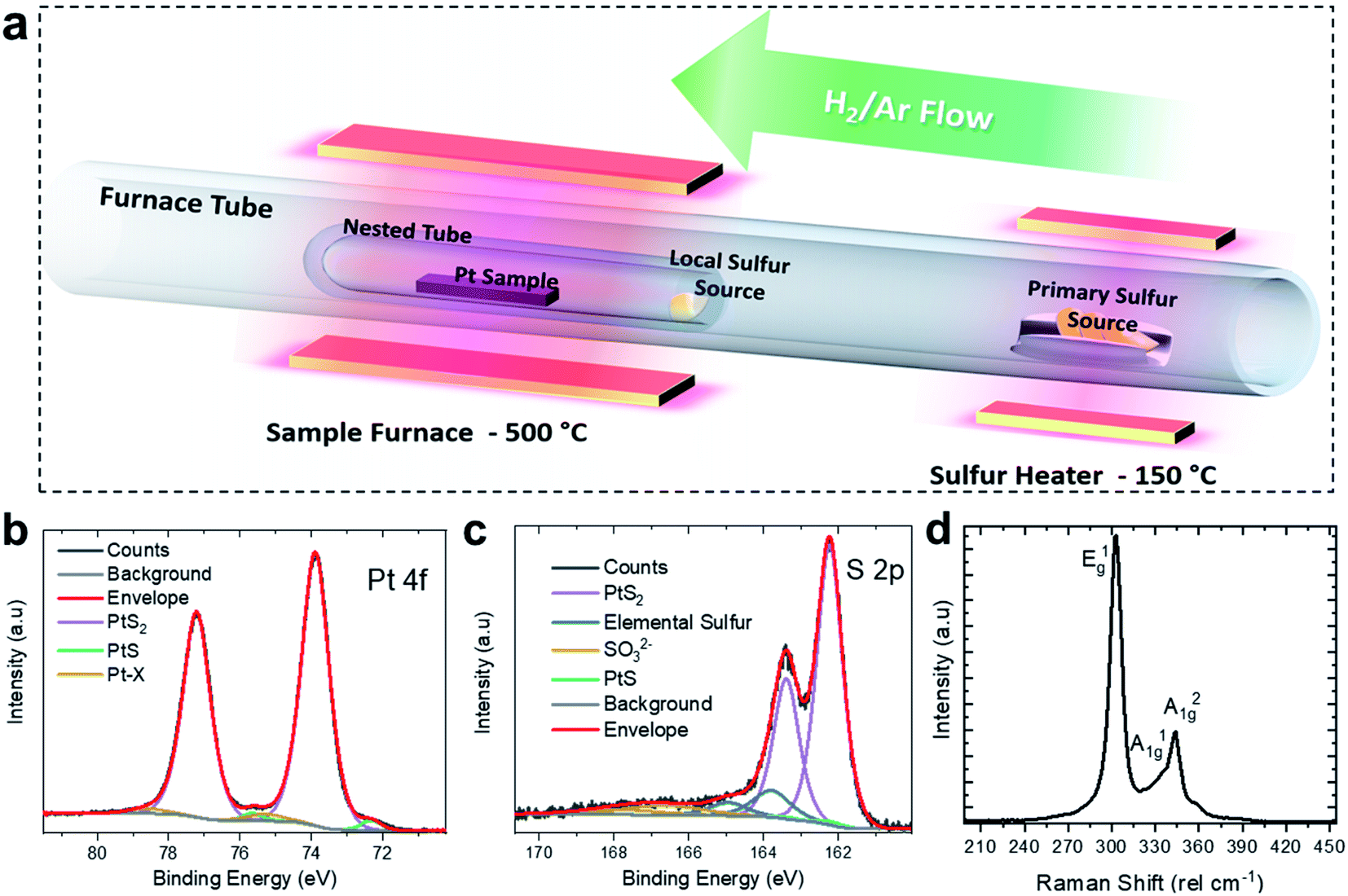 | ||
| Fig. 1 Characterization of the PtS2 film. (a) Schematic of the sulfurization process with the nested tube configuration. (b) & (c) Fitted XPS of PtS2 film demonstrating the Pt 4f and S 2p core levels respectively. (d) Raman spectrum of a PtS2 film presenting the three Raman-active vibrational modes. These two methods help to confirm the successful synthesis of PtS2. | ||
High-resolution XPS, Raman spectroscopy and X-ray diffraction (XRD) were utilised to confirm the synthesis of PtS2. The characteristic XPS core-levels for PtS2 are the Pt 4f and the S 2p (see Fig. 1(b) and (c)), both regions show dominant doublet pairs corresponding to PtS2. The Pt 4f7/2 peak is centred at 73.9 eV while the S 2p3/2 is at 162.2 eV, consistent with the expected values.48 From the fitting, the small shoulder at ∼72 eV is attributed to a low level of Pt(II) contribution. Comparing the relative peak areas of the PtS2 components yields a stoichiometry of PtS1.89.36 As noted earlier, a lack of sulfur during synthesis will result in the synthesis of PtS, but despite evidence of an excess of elemental sulfur, there are still indications of trace PtS present in the films. The formation of polycrystalline PtS2 is also supported by XRD of the thin-film, as shown in Fig. S1 of the ESI.†
Raman spectroscopy using 532 nm excitation yielded the spectrum shown in Fig. 1(d). PtS2 has three main characteristic Raman modes, all of which are clearly distinguishable in this spectrum. These are the out-of-plane E1g mode at 303 cm−1 and the in-plane modes A21g and A11g at 343 and ∼334 cm−1, respectively. The small shoulder ∼360 cm −1 is likely due to the polycrystalline nature of the film or the presence of PtS, as this feature is not observed for in the Raman spectra of exfoliated PtS2.24,31 Otherwise this spectrum is consistent with high-purity PtS2 with relatively small grain sizes yielding broader Raman peaks when compared to mechanically-exfoliated PtS2.24,31,36,49
3.2. STM and STS characterisation of 1T-PtS2
STM was used to investigate the atomic structure of the TAC-grown PtS2 film as shown in Fig. 2. The 1T atomic-structure model of PtS2 is schematically shown in Fig. 2(a) (side- and top-views). The large-area scan in Fig. 2(b) reveals that the films are polycrystalline consisting of crystalline grains (flakes) of PtS2 with approximate lateral dimensions up to 40 nm. The root-mean square (RMS) roughness of the image 2(b) is around 2.6 nm. Overall, the surface morphology is similar to that of TAC-grown PtSe2.50,51 It can be seen from Fig. 2(c) (area depicted in Fig. 2(b) by the blue square) that there are some atomically-clean areas on the surface of the flakes, as can be judged from the sharp straight edges of the flakes. This indicates the stability of the PtS2 during transfer, under ambient conditions, from the growth furnace to the STM chamber, which is in contrast with the behaviour of some 2D materials such as black phosphorous.52 However, some contamination is present on the surface, most likely due to the exposure to ambient conditions. The crystal angles observed advocate hexagonal symmetry, which implies the presence of PtS2, rather than cubic symmetry, which would suggest a significant presence of PtS.35,53 Fig. 2(d) displays an atomic-resolution image of the defect-free PtS2 surface (area indicated by the blue square in Fig. 2(c)), verifying the 1T crystal structure of the PtS2 grains.24,36 The in-plane interatomic distance and a monolayer step height for the PtS2 of 3.58 ± 0.03 Å and 5.5 ± 0.06 Å, respectively were obtained from this atomically-resolved STM images which is in good agreement with previous theoretical and experimental reports.24,27,30,32,54 The Fast Fourier Transform (FFT) of the atomically resolved STM image is presented in inset of Fig. 2(d): the surface exhibits clearly ordered structures with the (1 × 1) symmetry of PtS2. The spatial periodicity of a = 3.58 Å in the PtS2 crystal was measured from FFT. It should be noted that no surface preparation under UHV (annealing or ion sputtering) was carried out prior to STM/STS investigation.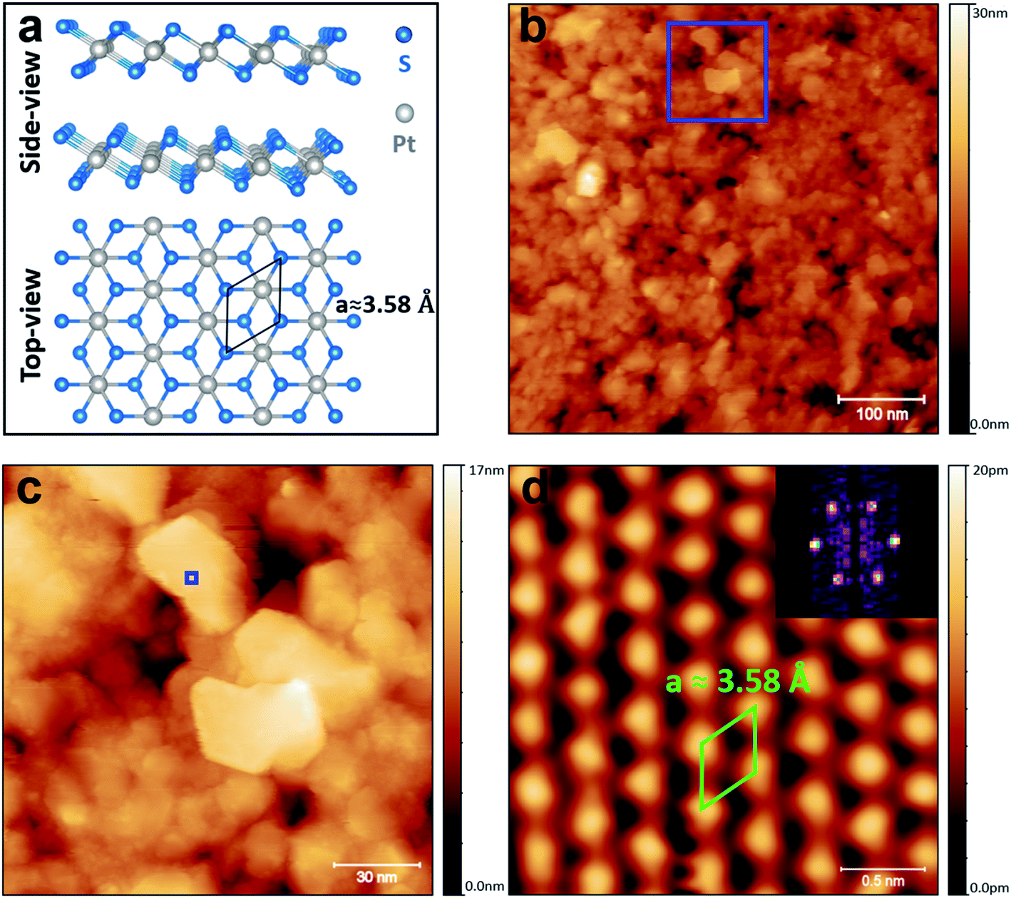 | ||
| Fig. 2 STM images of PtS2 film. (a) Structure model of 1T-PtS2 with side- and top-views. (b) Large-scale STM image of the PtS2 showing the polycrystalline film (500 × 500 nm2, V = 1.5 V and I = 120 pA). (c) STM image of the area which is depicted in (b) (blue box), demonstrating flakes of PtS2 with partially atomically-clean surface (150 × 150 nm2, V = 1.5 V and I = 120 pA). (d) Atomically-resolved STM image, with FFT inset, of the 1T-PtS2 surface indicates an interatomic distance of 3.58 ± 0.03 Å (2.5 × 2.5 nm2, V = 1.4 V and I = 400 pA). | ||
In order to understand the electronic nature of the TAC-grown PtS2, STS was used to map the local density of states (LDOS) on the pristine surface of PtS2. A large-scale STM image showing grains of PtS2 is shown in Fig. 3(a). The inset in Fig. 3(a) shows the line profile of the PtS2 flake (around 3.8 nm) where STS measurements were performed. It should be noted that thickness of the flake is an approximation since STM measures the density of states. Fig. 3(b) shows a high-resolution STM image (4 × 4 nm2) of the atomically clean PtS2 surface. Fig. 3(c) illustrates grid STS55 measurements performed on the same area as in Fig. 3(b). 40 × 40 individual I(V) measurements were conducted on the grid with dimensions of 4 × 4 nm2. At each point of the grid, the spectra were averaged over three individual I(V)-measurements. The tip was moved in constant-current mode with the scanning parameters V = 1.4 (V) and I = 400 (pA) between points. The small variation observed in the tunnelling current at different voltages is due to differences in the electronic structure. The voltage was swept between −1.45 V and + 2 V. Fig. 3(c) represents the tunnelling current from the I(V) at each spectroscopy point at a bias voltage value of −1.45 V. Slightly brighter points correspond to a higher tunnelling current value at −1.45 V. A pixelated outline of the atomically-resolved features can be observed from the grid STS in Fig. 3(c).
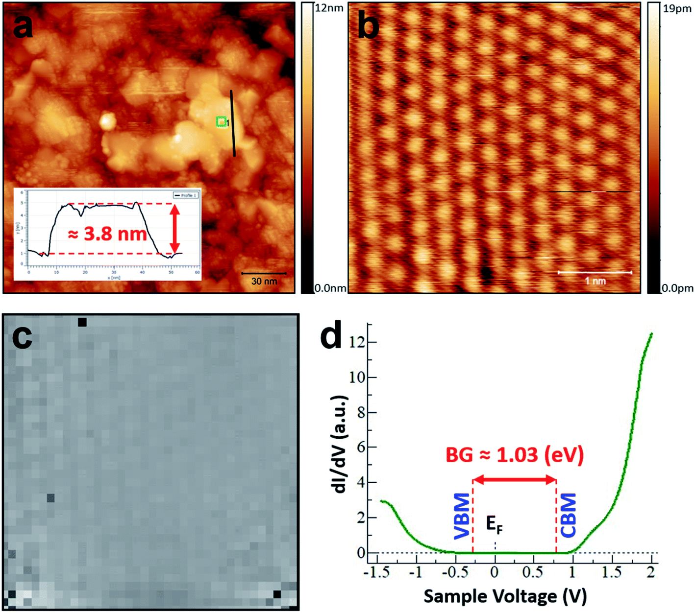 | ||
| Fig. 3 STS of PtS2 film. (a) Large-area STM image with ∼3.8 nm thick flake of PtS2 where STS analysis was performed. (b) Atomically-resolved STM image of the PtS2 surface (4 × 4 nm2, V = 1.4 V and I = 400 pA). A grid spectroscopy measurement was performed on the area depicted in (b). (c) 40 × 40 point grid spectroscopy measurement demonstrates the tunneling current value (taken from the I(V)) at each spectroscopy point on the grid at a bias voltage value of −1.45 V. (d) An averaged dI/dV spectra of the whole grid, which indicates that the bandgap is around 1.03 (eV). | ||
It is known that dI/dV spectra (numerical derivative of I(V)) are proportional to the LDOS. The averaged dI/dV spectrum, which was acquired on the pristine terrace of PtS2, is depicted in Fig. 3(d). The spectrum shown is an average of a few thousand individual spectra on the atomically clean surface. The VBM is positioned at 0.27 ± 0.02 eV below the Fermi level, and the CBM is positioned at 0.76 ± 0.02 eV above the Fermi level. Thus, the obtained bandgap of PtS2 here is around 1.03 (eV), which is slightly larger than the bandgap predicted for this thickness in theoretical studies.25,56 The LDOS of the PtS2 flake is sharp in the conduction band, while in the valence band the LDOS increases gradually. The relative location of the Fermi level with respect to the CBM and VBM reveals p-type semiconducting behaviour for our PtS2 flake.23,25 Such a bandgap would be suitable for many applications including thermoelectric devices31 and infrared photodetectors.27,28 The beauty of this material is that the bandgap can be tuned by controlling the thickness of the PtS2 film. Additionally, low-temperature synthesis of the PtS2 allows growth on diverse substrates, such as glass and polyimide,51,57 and thus broadens the potential application area. Our results establish that STM and STS are powerful techniques that can be applied to the characterisation of TAC-grown PtS2.
4. Conclusions
Our results verify that PtS2 can be preferentially grown by the TAC process and we have demonstrated that STM-based techniques can be applied to selectively investigate the atomic structure and electronic properties of polycrystalline PtS2 films synthesised in this way. XPS, XRD and Raman spectroscopy confirmed the successful growth of PtS2 with the correct stoichiometry. STM measurements allowed us to resolve the crystal structure of the TAC-grown PtS2 and determine a lattice constant of 3.58 ± 0.03 Å. The bandgap for a flake with thicknesses 3.8 nm, obtained via STS measurements, was found to be 1.03 eV. The relative position of the Fermi level indicated p-type semiconducting behaviour. These fundamental results can contribute to future studies focused on PtS2 and its application in devices.Conflicts of interest
There are no conflicts to declare.Acknowledgements
The authors appreciate the XPS assistance provided by Oliver Hartwig, Universität der Bundeswehr, and the PyC substrates supplied by Dr John McManus, Trinity College Dublin. I. V. S. acknowledges the support of SFI PI_12/IA/1264 and IRC LA (IRCLA/2019/171), G. S. D. and C. Ó C acknowledge the support of SFI under PI_15/IA/3131. N. M. acknowledges support from SFI through 15/SIRG/3329 and 12/RC/2278_P2. G. S. D acknowledges the European Commission under the project Queformal [829035] and the German Ministry of Education and Research (BMBF) under the project NobleNEMS [16ES1121]. K. Z. and A. Z. acknowledge the support of Government of Kazakhstan under the Bolashak program.References
- K. S. Novoselov, A. K. Geim, S. V. Morozov, D. Jiang, Y. Zhang, S. V. Dubonos, I. V. Grigorieva and A. A. Firsov, Electric Field Effect in Atomically Thin Carbon Films, Science, 2004, 306, 666–669 CrossRef CAS.
- C. Rubio-Verdú, A. M. García-García, H. Ryu, D.-J. Choi, J. Zaldívar, S. Tang, B. Fan, Z.-X. Shen, S.-K. Mo, J. I. Pascual and M. M. Ugeda, Visualization of multifractal superconductivity in a two-dimensional transition metal dichalcogenide in the weak disorder regime, Nano Lett., 2020, 20(7), 5111–5118 CrossRef.
- Y. Chen, W. Ruan, M. Wu, S. Tang, H. Ryu, H.-Z. Tsai, R. Lee, S. Kahn, F. Liou, C. Jia, O. R. Albertini, H. Xiong, T. Jia, Z. Liu, J. A. Sobota, A. Y. Liu, J. E. Moore, Z.-X. Shen, S. G. Louie, S.-K. Mo and M. F. Crommie, Strong correlations and orbital texture in single-layer 1T-TaSe2, Nat. Phys., 2020, 16, 218–224 Search PubMed.
- V. Yu. Aristov, A. N. Chaika, O. V. Molodtsova, S. V. Babenkov, A. Locatelli, T. O. Menteş, A. Sala, D. Potorochin, D. Marchenko, B. Murphy, B. Walls, K. Zhussupbekov and I. V. Shvets, Layer-by-Layer Graphene Growth on β-SiC/Si(001), ACS Nano, 2019, 13(1), 526–535 CrossRef CAS.
- B. Anasori, M. Lukatskaya and Y. Gogotsi, 2D metal carbides and nitrides (MXenes) for energy storage, Nat. Rev. Mater., 2017, 2, 16098 CrossRef CAS.
- V. Vyas, F. Haase and L. Stegbauer, et al., A tunable azine covalent organic framework platform for visible light-induced hydrogen generation, Nat. Commun., 2015, 6, 8508 CrossRef CAS.
- S. Goswami, S. Goswami and T. Venkatesan, An organic approach to low energy memory and brain inspired electronics, Appl. Phys. Rev., 2020, 7, 021303 CAS.
- S. Z. Butler, S. M. Hollen, L. Cao, Yi Cui, J. A. Gupta, H. R. Gutiérrez, T. F. Heinz, S. S. Hong, J. Huang, A. F. Ismach, E. J. Halperin, M. Kuno, V. V. Plashnitsa, R. D. Robinson, R. S. Ruoff, S. Salahuddin, J. han, Li Shi and M. G. Spencer, et al., Progress, Challenges, and Opportunities in Two-Dimensional Materials Beyond Graphene, ACS Nano, 2013, 7(no. 4), 2898–2926 CrossRef CAS.
- B. Schuler, D. Y. Qiu, S. Refaely-Abramson, C. Kastl, C. T. Chen, S. Barja, R. J. Koch, D. F. Ogletree, S. Aloni, A. M. Schwartzberg, J. B. Neaton, S. G. Louie and A. Weber-Bargioni, Large Spin-Orbit Splitting of Deep In-Gap Defect States of Engineered Sulfur Vacancies in Monolayer WS2, Phys. Rev. Lett., 2019, 123(7), 076801 CrossRef CAS.
- D. Edelberg, D. Rhodes, A. Kerelsky, B. Kim, J. Wang, A. Zangiabadi, C. Kim, A. Abhinandan, J. Ardelean, M. Scully, D. Scullion, L. Embon, R. Zu, E. J. G. Santos, L. Balicas, C. Marianetti, K. Barmak, X. Zhu, J. Hone and A. N. Pasupathy, Approaching the Intrinsic Limit in Transition Metal Diselenides via Point Defect Control, Nano Lett., 2019, 19(no. 7), 4371–4379 CrossRef CAS.
- S. Barja, S. Refaely-Abramson and B. Schuler, et al., Identifying substitutional oxygen as a prolific point defect in monolayer transition metal dichalcogenides, Nat. Commun., 2019, 10, 3382 CrossRef.
- L. Ansari, S. Monaghan, N. McEvoy, C. Ó Coileáin, C. P. Cullen, J. Lin, R. Siris, T. Stimpel-Lindner, K. F. Burke, G. Mirabelli, R. Duffy, E. Caruso, R. E. Nagle, G. S. Duesberg, P. K. Hurley and F. Gity, Quantum confinement-induced semimetal-to-semiconductor evolution in large-area ultra-thin PtSe2 films grown at 400 °C, npj 2D Mater. Appl., 2019, 3, 33 CrossRef.
- H. Ma, P. Chen, B. Li, J. Li, R. Ai, Z. Zhang, G. Sun, K. Yao, Z. Lin, B. Zhao, R. Wu, X. Tang, X. Duan and X. Duan, Thickness-Tunable Synthesis of Ultrathin Type-II Dirac Semimetal PtTe2 Single Crystals and Their Thickness-Dependent Electronic Properties, Nano Lett., 2018, 18(no. 6), 3523–3529 CrossRef CAS.
- S. Manzeli, D. Ovchinnikov, D. Pasquier, O. V. Yazyev and A. Kis, 2D transition metal dichalcogenides, Nat. Rev. Mater., 2017, 2, 17033 CrossRef CAS.
- Z. Pedramrazi, C. Herbig, A. Pulkin, S. Tang, M. Phillips, D. Wong, H. Ryu, M. Pizzochero, Y. Chen, F. Wang, E. J. Mele, Z.-X. Shen, S.-K. Mo, O. V. Yazyev and M. F. Crommie, Manipulating Topological Domain Boundaries in the Single-Layer Quantum Spin Hall Insulator 1T′–WSe2, Nano Lett., 2019, 19(no. 8), 5634–5639 CrossRef CAS.
- Q. Wang, K. Kalantar-Zadeh, A. Kis, J. N. Coleman and M. S. Strano, Electronics and optoelectronics of two-dimensional transition metal dichalcogenides, Nat. Nanotechnol., 2012, 7, 699–712 CrossRef CAS.
- N. Rohaizad, C. C. Mayorga-Martinez, Z. Sofer, R. D. Webster and M. Pumera, Layered platinum dichalcogenides (PtS2, PtSe2, PtTe2) for non-enzymatic electrochemical sensor, Appl. Mater. Today, 2020, 100606 CrossRef.
- J. B. McManus, D. Horvath, M. Browne, C. P Cullen, G. Cunningham, T. Hallam, K. Zhussupbekov, D. Mullarkey, C. O. Coileain, I. V. Shvets, M. Pumera, G. S. Duesberg and N. McEvoy, Low-temperature synthesis and electrocatalytic application of large-area PtTe2 thin films, Nanotechnology, 2020, 31(37), 375601 CrossRef CAS.
- R. Kempt, A. Kuc and T. Heine, Two-Dimensional Noble-Metal Chalcogenides and Phosphochalcogenides, Angew. Chem., Int. Ed., 2020, 59, 9242–9254 CrossRef CAS.
- Y.-H. Lee, X.-Q. Zhang, W. Zhang, M.-T. Chang, C.-T. Lin, K.-D. Chang, Y.-C. Yu, J. T.-W. Wang, C.-S. Chang, L.-J. Li and T.-W. Lin, Synthesis of Large-Area MoS2 Atomic Layers with Chemical Vapor Deposition, Adv. Mater., 2012, 24(no. 17), 2320–2325 CrossRef CAS.
- C.-P. Lu, G. Li, J. Mao, L.-M. Wang and E. Y. Andrei, Bandgap, Mid-Gap States, and Gating Effects in MoS2, Nano Lett., 2014, 14(no. 8), 4628–4633 CrossRef CAS.
- X. Chia, A. Adriano, P. Lazar, Z. Sofer, J. Luxa and M. Pumera, Layered Platinum Dichalcogenides (PtS2, PtSe2, and PtTe2) Electrocatalysis: Monotonic Dependence on the Chalcogen Size, Adv. Funct. Mater., 2016, 26, 4306–4318 CrossRef CAS.
- D. Zhao, S. Xie, Y. Wang, H. Zhu, L. Chen, Q. Sun and D. W. Zhang, Synthesis of large-scale few-layer PtS2 films by chemical vapor deposition, AIP Adv., 2019, 9, 025225 CrossRef.
- Y. Zhao, J. Qiao, P. Yu, Z. Hu, Z. Lin, S. P. Lau, Z. Liu, W. Ji and Y. Chai, Extraordinarily Strong Interlayer Interaction in 2D Layered PtS2, Adv. Mater., 2016, 28, 2399–2407 CrossRef CAS.
- R. A. B. Villaos, C. P. Crisostomo, Z. Huang, S.-M. Huang, A. A. B. Padama, M. A. Albao, H. Lin and F.-C. Chuang, Thickness dependent electronic properties of Pt dichalcogenides, npj 2D Mater. Appl., 2019, 3, 2 CrossRef.
- K. Iordanidou, M. Houssab and C. Perssona, Carrier-mediated ferromagnetism in two-dimensional PtS2, RSC Adv., 2020, 10, 952–957 RSC.
- L. Li, W. Wang, Y. Chai, H. Li, M. Tian and T. Zhai, Few-Layered PtS2 Phototransistor on h-BN with High Gain, Adv. Funct. Mater., 2107, 27, 1701011 CrossRef.
- J. Yuan, T. Sun, Z. Hu, W. Yu, W. Ma, K. Zhang, B. Sun, S. P. Lau, Q. Bao, S. Lin and S. Li, Wafer-Scale Fabrication of Two-Dimensional PtS2/PtSe2 Heterojunctions for Efficient and Broad band Photodetection, ACS Appl. Mater. Interfaces, 2018, 10(47), 40614–40622 CrossRef CAS.
- L. Cai, N. Zhang, B. Qiu and Y. Chai, Computational Design of Transition Metal Single Atom Electrocatalysts on PtS2 for Efficient Nitrogen Reduction, ACS Appl. Mater. Interfaces, 2020, 12(18), 20448–20455 CrossRef CAS.
- H. L. Zhuang and R. G. Hennig, Computational Search for Single-Layer Transition-Metal, J. Phys. Chem. C, 2013, 117, 20440–20445 CrossRef CAS.
- L. Pi, L. Li, X. Hu, S. Zhou, H. Li and T. Zhai, Temperature dependence of Raman responses of few-layer PtS2, Nanotechnology, 2018, 29, 505709 CrossRef.
- H. Long, C. Y. Tang, P. K. Cheng, X. Y. Wang, W. Qarony and Y. H. Tsang, Ultrafast laser pulses generation by using 2D layered PtS2 as a saturable absorber, J. Lightwave Technol., 2019, 37, 1174–1179 CAS.
- E. Davy Esq., On the combinations of sulphur and phosphorus with platina, Philos. Mag., 1812, VII, 27–39 CrossRef.
- F. Gronvold, H. Haraldsen and A. Kjekshus, On the Sulfides, Selenides and Tellurides of Platinum, Acta Chem. Scand., 1960, 14, 1879–1893 CrossRef.
- J. Huang, N. Dong, N. McEvoy, L. Wang, C. Ó. Coileáin, H. Wang, C. P. Cullen, C. Chen, S. Zhang, L. Zhang and J. Wang, Surface-State Assisted Carrier Recombination and Optical Nonlinearities in Bulk to 2D Nonlayered PtS, ACS Nano, 2019, 13(11), 13390–13402 CrossRef CAS.
- H. Xu, H.-P. Huang, H. F. Fei, J. Feng, H.-R. Fuh, J. Cho, M. Choi, Y. Chen, L. Zhang, D. Chen, D. Zhang, C. Ó. Coileáin, X. Han, C.-R. Chang and H.-C. Wu, Strategy for Fabricating Wafer-Scale Platinum Disulfide, ACS Appl. Mater. Interfaces, 2019, 11(8), 8202–8209 CrossRef CAS.
- H. P. Komsa, S. Kurasch, O. Lehtinen, U. Kaiser and A. V. Krasheninnikov, From point to extended defects in two-dimensional MoS2: evolution of atomic structure under electron irradiation, Phys. Rev. B: Condens. Matter Mater. Phys., 2013, 88, 035301 CrossRef.
- J. Hong, Z. Hu, M. Probert, K. Li, D. Lv, X. Yang, L. Gu, N. Mao, Q. Feng, L. Xie, J. Zhang, D. Wu, Z. Zhang, C. Jin, W. Ji, X. Zhang, J. Yuan and Z. Zhang, Exploring atomic defects in molybdenum disulphide monolayers, Nat. Commun., 2015, 6, 6293 CrossRef CAS.
- S. Wang, A. Robertson and J. H. Warner, Atomic structure of defects and dopants in 2D layered transition metal dichalcogenides, Chem. Soc. Rev., 2018, 47, 6764–6794 RSC.
- J. Osing and I. V. Shvets, Bulk defects in graphite observed with a scanning tunnelling microscope, Surf. Sci., 1998, 417(no. 1), 145–150 CrossRef CAS.
- H. Zheng, Y. Choi, F. Baniasadi, D. Hu, L. Jiao, K. Park and C. Tao, Visualization of point defects in ultrathin layered 1T-PtSe2, 2D Mater., 2019, 6, 041005 CrossRef CAS.
- A. S. Frolov, A. S. Frolov, J. Sánchez-Barriga, C. Callaert, J. Hadermann, A. V. Fedorov, D. Yu. Usachov, A. N. Chaika, B. C. Walls, K. Zhussupbekov, I. V. Shvets, M. Muntwiler, M. Amati, L. Gregoratti, A. Yu. Varykhalov, O. Rader and L. V. Yashina, Atomic and Electronic Structure of a Multidomain GeTe Crystal, ACS Nano, 2020 DOI:10.1021/acsnano.0c05851.
- C. Xie, S. Jiang, Y. Gao, M. Hong, S. Pan, J. Zhao and Y. Zhang, Giant Thickness-Tunable Bandgap and Robust Air Stability of 2D Palladium Diselenide, Small, 2020, 16, 2000754 CrossRef CAS.
- N. McEvoy, N. Peltekis, S. Kumar, E. Rezvani, H. Nolan, G. P. Keeley, W. J. Blau and G. S. Duesberg, Synthesis and analysis of thin conducting pyrolytic carbon films, Carbon, 2012, 50(3), 1216–1226 CrossRef CAS.
- C. Dong, G. Meng, S. E. Saji, X. Gao, P. Zhang, D. Wu, Yi Pan, Z. Yin and Y. Cheng, Simulation-guided nanofabrication of high-quality practical tungsten probes, RSC Adv., 2020, 10, 24280–24287 RSC.
- H. R. Gutiérrez, N. Perea-López, A. L. Elías, A. Berkdemir, B. Wang, R. Lv, F. López-Urías, V. H. Crespi, H. Terrones and M. Terrones, Extraordinary Room-Temperature Photoluminescence in Triangular WS2 Monolayers, Nano Lett., 2013, 13(no. 8), 3447–3454 CrossRef.
- C. Yim, K. Lee, N. McEvoy, M. O'Brien, S. Riazimehr, N. C. Berner, C. P. Cullen, J. Kotakoski, J. C. Meyer, M. C. Lemme and G. S. Duesberg, High-Performance Hybrid Electronic Devices from Layered PtSe2 Films Grown at Low Temperature, ACS Nano, 2016, 10(no. 10), 9550–9558 CrossRef CAS.
- J. Dembowski, L. Marosi and M. Essig, Platinum Disulfide by XPS, Surf. Sci. Spectra, 1993, 2, 133–137 CrossRef CAS.
- D. Caffrey, A. Zhussupbekova, R. K. Vijayaraghavan, A. Ainabayev, A. Kaisha, G. Sugurbekova, I. V. Shvets and K. Fleischer, Crystallographic Characterisation of Ultra-Thin, or Amorphous Transparent Conducting Oxides—The Case for Raman Spectroscopy, Materials, 2020, 13(no. 2), 267 CrossRef CAS.
- C. Yim, V. Passi, M. C. Lemme, G. S. Duesberg, C. Ó Coileáin, E. Pallecchi, D. Fadil and N. McEvoy, Electrical devices from top-down structured platinum diselenide films, npj 2D Mater. Appl., 2018, 2, 5 CrossRef.
- C. S. Boland, C. Ó. Coileáin, S. Wagner, J. B. McManus, C. P. Cullen, M. C. Lemme, G. S. Duesberg and N. McEvoy, PtSe2 grown directly on polymer foil for use as a robust piezoresistive sensor, 2D Materials, 2019, 6(4), 045029 CrossRef CAS.
- J. O. Island, G. A. Steele, H. S. J. van der Zant and A. Castellanos-Gomez, Environmental instability of few-layer black phosphorus, 2D Materials, 2015, 2(1), 011002 CrossRef.
- V. I. Rozhdestvina, A. A. Udovenko, S. V. Rubanov and N. V. Mudrovskaya, Structural Investigation of Cooperite (PtS) Crystals, Crystallogr. Rep., 2016, 61, 193–202 CrossRef CAS.
- S. Furuseth, K. Selte and A. Kjekshus, Redetermined crystal structures of NiTe2, PdTe2, PtS2, PtSe2, and PtTe2, Acta Chem. Scand., 1065, 19, 257–258 CrossRef.
- K. Zhussupbekov, K. Walshe, S. I. Bozhko, A. Ionov, K. Fleischer, E. Norton, A. Zhussupbekova, V. Semenov, I. V. Shvets and B. Walls, Oxidation of Nb(110): atomic structure of the NbO layer and its influence on further oxidation, Sci. Rep., 2020, 10, 3794 CrossRef CAS.
- S. Liu, H. Zhu, Z. Liu and G. Zhou, Symmetrical metallic and magnetic edge states of nanoribbon from semiconductive monolayer PtS2, Phys. Lett. A, 2018, 382(no. 11), 776–780 CrossRef CAS.
- E. Okogbue, S. S. Han, T.-J. Ko, H.-S. Chung, J. Ma, M. S. Shawkat, J. H. Kim, J. H. Kim, E. Ji, K. H. Oh, L. Zhai, G.-H. Lee and Y. Jung, Multifunctional Two-Dimensional PtSe2-Layer Kirigami Conductors with 2000% Stretchability and Metallic-to-Semiconducting Tunability, Nano Lett., 2019, 19(no. 11), 7598–7607 CrossRef CAS.
Footnote |
| † Electronic supplementary information (ESI) available. See DOI: 10.1039/d0ra07405e |
| This journal is © The Royal Society of Chemistry 2020 |