
 Open Access Article
 This Open Access Article is licensed under a
 Creative Commons Attribution 3.0 Unported Licence
Anisotropic quasi-one-dimensional layered transition-metal trichalcogenides: synthesis, properties and applications†
Abhinandan Patra
and
Chandra Sekhar Rout
 *
*
Centre for Nano and Material Sciences, Jain University, Jain Global Campus, Jakkasandra, Ramanagaram, Bangalore-562112, India. E-mail: r.chandrasekhar@jainuniversity.ac.in; csrout@gmail.com
First published on 2nd October 2020
Abstract
The strong in-plane anisotropy and quasi-1D electronic structures of transition-metal trichalcogenides (MX3; M = group IV or V transition metal; X = S, Se, or Te) have pronounced influence on moulding the properties of MX3 materials. In particular, the infinite trigonal MX6 prismatic chains running parallel to the b-axis are responsible for the manifestation of anisotropy in these materials. Several marvellous properties, such as inherent electronic, optical, electrical, magnetic, superconductivity, and charge density wave (CDW) transport properties, make transition-metal trichalcogenides (TMTCs) stand out from other 2D materials in the fields of nanoscience and materials science. In addition, with the assistance of pressure, temperature, and tensile strain, these materials and their exceptional properties can be tuned to a superior extent. The robust anisotropy and incommensurable properties make the MX3 family fit for accomplishing quite a lot of compelling applications in the areas of field effect transistors (FETs), solar and fuel cells, lithium-ion batteries, thermoelectricity, etc. In this review article, a precise audit of the distinctive crystal structures, static and dynamic properties, efficacious synthesis schemes, and enthralling applications of quasi-1D MX3 materials is made.
 Abhinandan Patra | Abhinandan Patra received his M.Sc. degree in Physics from the College of Engineering and Technology under Biju Patnaik University of Technology (BPUT), Odisha, India, in 2019. He is presently pursuing his PhD degree at the Centre for Nano and Material Sciences, Jain University. His main research interests are the synthesis and comprehensive characterization of novel functionalized layered 2D nanomaterials and their composites for electrochemical storage and conversion applications. |
 Chandra Sekhar Rout | Dr Chandra Sekhar Rout is Associate Professor at the Centre for Nano & Material Sciences, Jain University. Before joining CNMS, he was a DST-Ramanujan Fellow at IIT Bhubaneswar, India (2013–2017). He received his B.Sc. (2001) and M.Sc. (2003) degrees from Utkal University and his PhD from JNCASR, Bangalore (2008) under the supervision of Prof. C. N. R. Rao. He did postdoctoral research at National University of Singapore (2008–2009), Purdue University, USA (2010–2012), and UNIST, South Korea (2012–2013). His research interests include 2D materials for sensors, supercapacitors and energy storage devices, field emitters, and electronic devices. |
1. Introduction
The many pioneering studies based on the modern miracle material graphene1 paved the way for other monolayered and few-layered two-dimensional transition metal dichalcogenides (TMDCs) to be studied. They gained huge attention due to their strong tunable mechanical, electrical, optical, and physiochemical properties originating from the low dimensionality and quantum confinement effects. In accordance with the above excellent properties, they are useful for various optoelectronic and energy storage applications. Another noteworthy family of two-dimensional materials is transition metal trichalcogenides (MX3), which have been a source of attraction for a couple of years. These MX3 materials possess typical electrical, optical, magnetic, and physical properties that are quite anisotropic. Therefore, linking the benefits of 2D materials (elasticity, robustness, ease of synthesis, and huge surface to volume ratios) with excellent quasi-one-dimensional (1D) properties can be reasonably fruitful for application in the unexplored directions of nanoelectronics and nanotechnology.The weak van der Waals amalgamated crystal structures of MX3 architecturally and chemically constitute a very distinct family of compounds, where M (group IV, V, or VI) represents a metal atom and X is a chalcogen atom (S, Se, or Te), and the M–X bond is ionic–covalent in nature.6–9 The compact in-plane anisotropy and quasi one-dimensional properties of monolayer and few-layer MX3 contribute a huge amount to configuring every single property of these materials. The prismatic MX6 chains of MX3 are extended along the b-axis to provide strong anisotropy. Pressure, temperature, and tensile strain can tune the electronic properties, and charge density wave transportation plays a pivotal role in making metal trichalcogenides a prime material of interest in the nanoscience and materials science communities. Instead of bulk or layered MX3, monolayer metal trichalcogenides are of considerable interest in both experimental and theoretical investigations. Monolayer TiS3 and TaS3, fabricated through mechanical exfoliation, show amazing superconductivity and charge density wave phenomena. This breakthrough accounts for their pronounced, unparalleled, and plentiful applications in the field of nanoelectronics.
Wide amounts of research have been ongoing concerning the flexible fabrication of MX3 materials, and attempts to shed several layers to obtain monolayers have also been made in the past few years through many emerging top-down synthesis methods. These new-fangled methods include chemical vapour deposition (CVD), chemical vapour transport (CVT), solvothermal methods, mechanical and chemical exfoliation, etc. As far as this review is concerned, we report cumulative information regarding crystal structures, elementary properties, synthesis procedures, applications, and experimental and theoretical developments related to MX3-based materials. Firstly, emblematic crystal structures and typical electrical, optical, magnetic, and CDW transport property characteristics are thoroughly discussed. Secondly, the fabrication of these materials is looked into. Lastly, the wide variety of applications of MX3, including field emission transistors,124–126,142 solar and fuel cells,139,143–148 photo-detectors and -sensors,33,139,150,151 lithium ion batteries,134,152–155 and thermoelectricity,156–161 are discussed with proper reference to previous studies.
2. Classification and crystal structures of MX3
Layered MX3 materials have emerged as a modern development with interesting electrical and optical properties due to their in-plane anisotropy.2–4 With robust structural in-plane anisotropy, MX3 materials combine the boons of both 2D layered material properties and quasi-1D material properties. Materials in the MX3 family are fascinating candidates for this purpose due to their reduced in-plane bonding symmetry.2–4 These MX3 materials can be classified into three categories (IV–X, V–X, VI–X) based on the metal (M) position in the periodic table. Here, X is the chalcogen element (S, Se, or Te); group IV elements are Ti, Zr, Hf, and Rf; group V elements are V, Nb, Ta, and Db; and group VI elements are Cr, Mo, W, and Sg. Among these materials, VI–X materials are reported to be amorphous5 and are less reported in the literature. A brief overview of the classification, crystal structures, and properties of widely studied MX3 materials (IV–X, V–X) is provided in Table 1.| Group | Transition metal | S | Se | Te |
|---|---|---|---|---|
| IV | Ti | Monoclinic | No report | No report |
| a = 4.973 Å, b = 3.433 Å, c = 8.714 Å; β = 97.74° | ||||
| Diamagnetic; n-type semiconductor; band gap: 0.8–1 eV; Hall mobility: 30 cm2 V−1 s−1 (ref. 2 and 12) | ||||
| Zr | Monoclinic | Monoclinic | Monoclinic | |
| a = 5.06 Å, b = 3.6 Å, c = 8.95 Å; β = 98.4° | a = 5.411 Å, b = 3.749 Å, c = 9.44 Å; β = 97.45° | a = 5.863 Å, b = 3.923 Å, c = 10.089 Å; β = 97.74° | ||
| Diamagnetic; p-type semiconductor; band gap: 1.8–2.5 eV; Hall mobility: 26 cm2 V−1 s−1 (ref. 12 and 52) | Diamagnetic; n-type semiconductor; band gap: 1.1 eV; Hall mobility: 3.9 cm2 V−1 s−1 (ref. 29 and 164) | Semi-metallic; TCDW = 63 K; Tc (superconductor) = 2 K (ref. 13 and 165) | ||
| Hf | Monoclinic | Monoclinic | Monoclinic | |
| a = 5.08 Å, b = 3.58 Å, c = 8.96 Å; β = 98.4° | a = 5.31 Å, b = 3.73 Å, c = 9.525 Å; β = 97.18° | a = 5.879 Å, b = 3.902 Å, c = 10.056 Å; β = 97.98° | ||
| Diamagnetic; p-type semiconductor; band gap: 1.9–3.1 eV; Hall mobility: 26 cm2 V−1 s−1 (ref. 52 and 165) | Diamagnetic; p-type semiconductor; band gap: 1.0 eV (ref. 3 and 7) | Semi-metallic; TCDW = 93 K; Tc (superconductor) = 4.3 K (ref. 151 and 166) | ||
| V | Nb | Triclinic | Monoclinic | No report |
| a = 4.963 Å, b = 6.730 Å, c = 9.144 Å; β = 97.17° | a = 10.009 Å, b = 3.48 Å, c = 15.629 Å; β = 109.47° | |||
| Diamagnetic; semiconductor; band gap: 0.8–1.1 eV (ref. 55 and 83) | Metal; TCDW = 145 K and 59 K (ref. 75, 79, 94 and 164) | |||
| Monoclinic | ||||
| a = 9.68 Å, b = 3.37 Å, c = 14.83 Å; β = 109.9° | ||||
| Diamagnetic; semiconductor; band gap: 0.3–1.0 eV; Hall mobility: 10–2400 cm2 V−1 s−1 (ref. 12 and 13) | ||||
| Ta | Orthorhombic | Monoclinic | No report | |
| a = 36.804 Å, b = 15.173 Å, c = 3.34 Å | a = 10.402 Å, b = 3.495 Å, c = 9.829 Å; β = 106.26° | |||
| Metal8 | Metal; superconductor; Tc = 2.1 K (ref. 55, 79 and 164) | |||
| Monoclinic | ||||
| a = 9.515 Å, b = 3.3412 Å, c = 14.912 Å; β = 109.99° | ||||
| Metal166 |
In most transition metal trichalcogenides, MX6 trigonal prisms (M as the central atom and X dwelling in the prism triangular base) are stacked so as to obtain MX3 trigonal prismatic chains, and these chains (aligned parallel to the b-axis of the unit cell) are covalently bonded through van der Waals forces [Fig. 1a].6 Due to this, these chalcogenides have the tendency to show 1D characteristics along with anisotropy. Depending on the X–X bond lengths in these MX3 crystals, three types of chain arrangement are possible,2–4 which are outlined below:
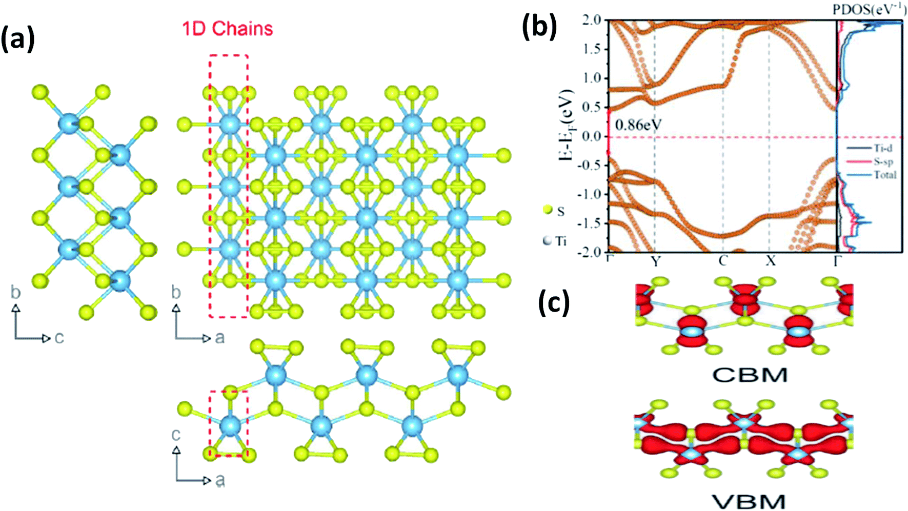 | ||
| Fig. 1 (a) The crystal structure of anisotropic TiS3 indicating the bond lengths between titanium and sulfur along the b-axis and a-axis, with shorter bonds along the b-axis; reproduced with permission from ref. 6, copyright: 2015, Springer Nature. (b) The calculated electronic energy band structure along the symmetry directions of the Brillouin zone (Γ–Y–C–X–Γ) and the projected density of states (PDOS) of the optimized structure of ML TiS3. The direct band gap Eg of ML TiS3 is indicated by the red arrows. The Fermi level is set to zero energy (the dashed line); reprinted with permission from ref. 8, copyright: 2019, American Chemical Society. (c) The charge distributions of the VBM and CBM states of monolayer TiS3; republished with permission from ref. 9, permission conveyed through Copyright Clearance Center, Inc. | ||
➢ A one-type chain arrangement is present in ZrSe3, with Se–Se bond lengths of 0.234 nm and (Se2)2− pairs forming in the trigonal base.
➢ A two-type chain arrangement is present in TaSe3, with Se–Se bond lengths of 0.258 nm and 0.291 nm (exceeding the value of ZrSe3). TiS3 crystals are an example of this type, with the arrangement: Ti4+S2−(S2)2−.
➢ A three-type chain arrangement is present in NbSe3 unit cells, with three Se–Se bonds at the base of the trigonal prismatic chains, short (III), mean (I), and long (II), having bond lengths of 0.237 nm, 0.248 nm, and 0.291 nm, respectively. The short bond length (0.237 nm) is ascribed to (Se2)2−, which supports the weakening of bonds between two Se atoms and strengthens the bonds between Nb and Se atoms. These types of arrangement create an intermediate situation with Nb4+ and Nb5+.
2.1. Crystal structures and properties of IV–X type MX3
As shown in Table 1, TiX3, ZrX3, and HfX3 (X = S, Se, or Te) are in the group-IV–X family, falling into the P21/m space group, and have been investigated for their remarkable physical and chemical properties. Of these, the crystal and band structures of TiS3 are shown in Fig. 1a–c.6,8,9 Different Ti–S bond lengths along the a (2.65 Å) and b (2.45 Å) axes consequently result in highly conducting 1D chains parallel to the b-axis and turn out to be the reason for the solid anisotropic properties.2,7 In Fig. 1b,8 the red dashed lines show the Ti one-dimensional chain, which is also covalently bonded laterally with the a-axis, materializing sheets and networks through van der Waals forces. The unit cell of monolayer TiS3 is supposed to be a rectangle, whereas for bulk TiS3, it is a monoclinic crystal with the measured lattice constants of a = 4.973 Å, b = 3.433 Å, c = 8.714 Å, and β = 97.74°.2,6 The nuclear binding energy of bulk TiS3 is ∼0.22 per unit cell.6,10,11 Significantly, there are no reports on TiSe3 and TiTe3.All members of the ZrX3 and HfX3 family take the form of monoclinic crystals, whose lattice parameters are summarized in Table 1. As discussed, the layered-type crystal structure of MX3 has the metal ion (M) in the centre of a slanted trigonal prism; stacked trigonal faces form separated columns that arrange along the b-axis, and the base triangle has a shape with two sides much longer than the third one.12–15 This criterion is satisfied by the formulation (X2−)(X22−), with the metal oxidation state being M4+ (d0), leading to empty d-block bands. Due to this fact, most MX3 compounds are reported to be semiconducting, with a band gap of ∼1–2 eV, except ZrTe3 and HfTe3, which are semi-metallic with superconducting properties at low temperatures.12–15 The crystal structure of ZrTe3 is presented in Fig. 4a and b.15
Experimental reports by Khatibi et al. showed that TiS3 emits near infrared (NIR) light centred at about 0.91 eV (1360 nm) with undeviated polarized anisotropic photoluminescence with a radiation life span of 210 ps (Fig. 2a–d).18 The dependence of emission on the excitation power and temperature demonstrated the dominant behaviour of free and bound electron–hole pairs over excitonic radiation at room and low temperature, correspondingly. TiS3 is reported to show excellent stable emission compared to other 2D materials, such as black phosphorus, MoTe2, etc.18 TiS3 is one of the appealing materials in the MX3 family due to its anisotropic optical properties. By using a force field along either the a-axis or b-axis and carrying out detection at intermediate angles between a and b, the anisotropic optical properties of 2D TiS3 are investigated.6 The anisotropic optical properties survey demonstrated strong emission anisotropy along the b-axis (25% higher emission intensity than along the a-axis). Island et al. inspected the strong in-plane anisotropy of TiS3 through angle-resolved polarization Raman spectroscopy (ARPRS).6 Compared to at room temperature, at 25 K, the in-plane conductivity in terms of anisotropy increases 2.09-fold. Fig. 2e and f6 shows Raman studies of TiS3 ribbons under different polarization conditions. Taking the b-axis as the favourable growth axis, four distinguishable Raman peaks (excluding one peak due to the silicon substrate) due to TiS3 were observed from an isolated nanoribbon on the SiO2/Si substrate. It is reported that the intensities of all the modes can be altered via changing the polarization angle, whereas the peak close to 370 cm−1 is found to be reliant on alignment between the polarization of the excitation laser and the b-axis. Furthermore, the anisotropy of the photosensitivity is verified based on the transmission of TiS3 through characteristic angles (Fig. 2h).6 The transmission reached a minimum value when the angle between the polarized excitation light source and the elongated side of the flakes was 180° (parallel to each other) in correspondence with the b-axis. The collected optical transmission data confirmed that TiS3 flakes exhibit robust linear dichroism, where the properties along the b-axis dominate those of the a-axis by as much as 30-fold, which is commendable for a 2D material.6 Compared to common semiconductors and other 2D TMDCs, TiS3 nanoribbons have a high exciton binding energy, which makes them an excellent applicant for use in optoelectronic devices and various related applications. Iyikanat et al. calculated the band gap of TiS3 using the PBE (Perdew–Burke–Ernzerhof) approximation and HSE06 (Heyd–Scuseria–Ernzerhof functional) correction to be 0.23 eV and 1.05 eV, respectively.19 The effects of S, Ti, TiS, and double S vacancies in TiS3 on its optical and electrical properties were also discussed based on DFT calculations by the above group (Fig. 3a–d).19 Of the four types of vacancies, except for S vacancies, the others lose their semiconducting properties and become metallic, resulting in a net magnetic moment. However, the low formation energy in the case of S vacancies assists in the opening of the energy gap of TiS3 monolayers. The calculated magnetic moments for the Ti, TiS, and double S vacancies of TiS3 are found to be 0.5, 0.8, and 0.3 μB per supercell, respectively.19 Kang et al. reported that the microelectronic properties of TiS3 nanoribbons strongly depend on the side, whether it is a or b.20 a-TiS3 nanoribbons are reported to have the properties of a metal, having a width-dependent band gap, whereas b-TiS3 is a semiconductor with a direct energy gap, which can be regulated by strain, is nearly self-governing, and does not hinge on the ribbon width.20
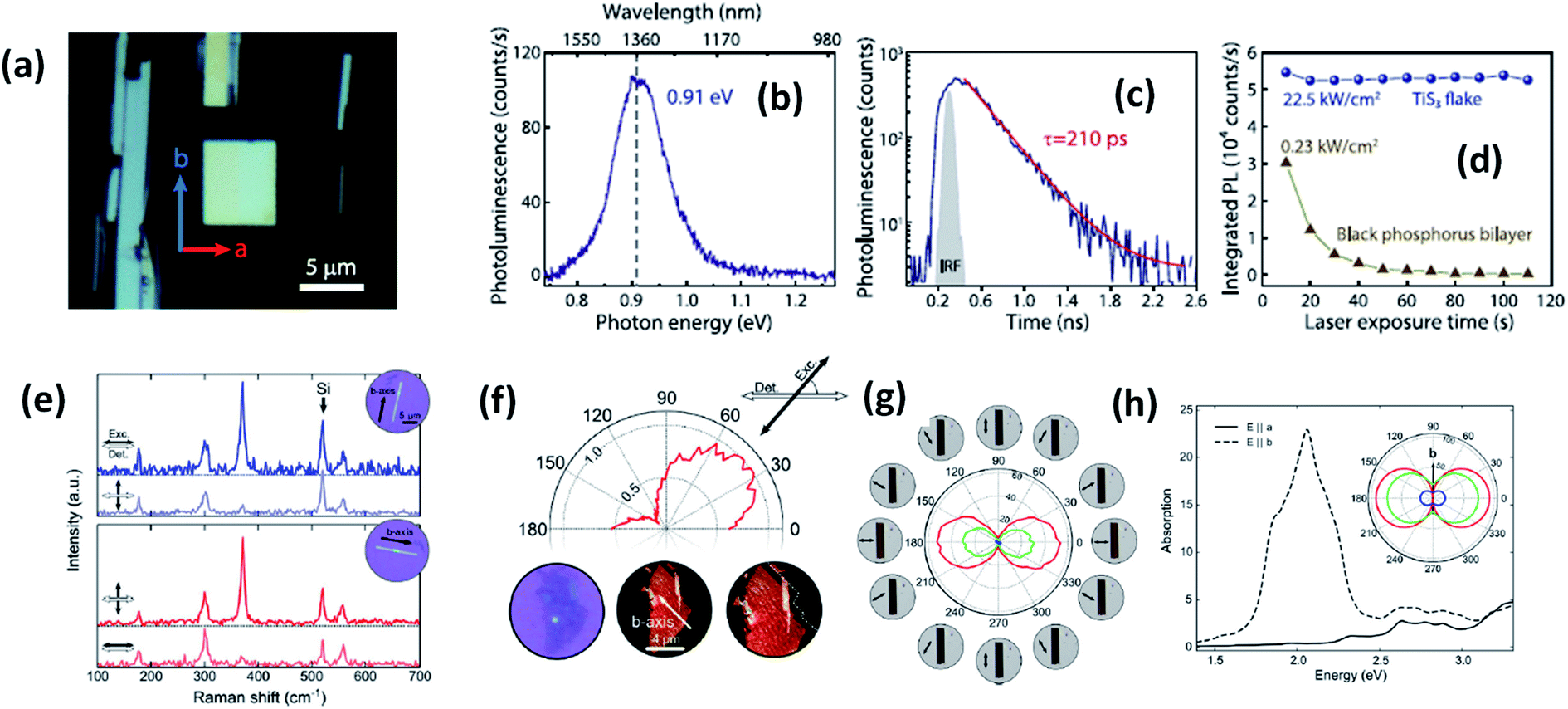 | ||
| Fig. 2 The optical properties of TiS3 flakes. (a) An optical microscope image showing the a and b axis directions and infrared light emission from TiS3. (b) Photoluminescence and (c) time-resolved photoluminescence spectra and (d) the photostability of a TiS3 flake compared to black phosphorus. Reproduced with permission from ref. 18, copyright: 2019, IOP Science. (e) Raman spectra of TiS3 ribbons with horizontal excitation and detection polarization. (f) The intensity of the 370 cm−1 Raman peak of a 3 nm-thick flake (3–4 layers) as a function of the excitation polarization angle (ref. 18). (g) The transmittance of the red, green, and blue channels as a function of the excitation polarization angle. (h) Calculated absorption spectra when the field is aligned parallel to the b-axis (dashed line) and the a-axis (solid line) with the inset showing the transmittance in the a–b plane for red (1.9 eV), green (2.4 eV), and blue (2.72 eV) excitation energies. Reproduced with permission from ref. 6; copyright: 2015, Springer Nature. | ||
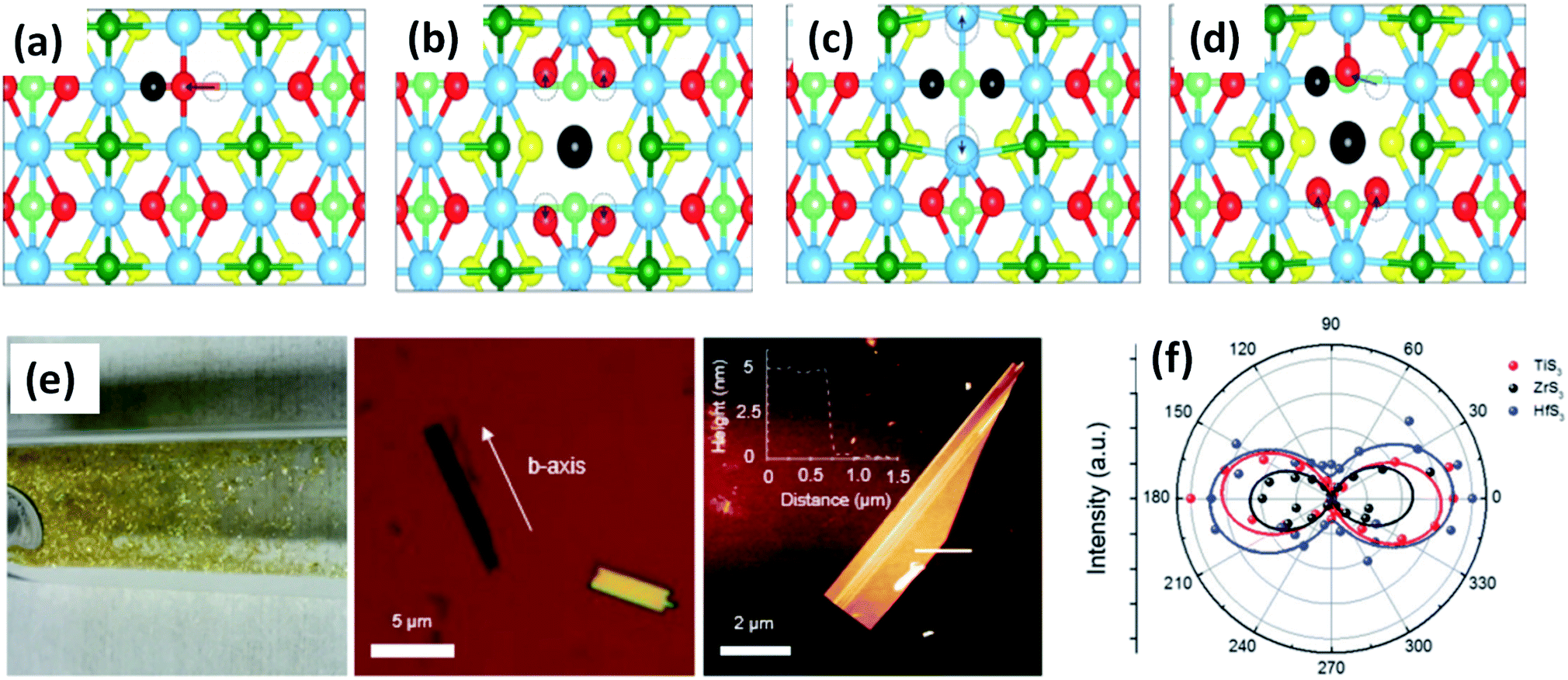 | ||
| Fig. 3 Top views of relaxed monolayer TiS3 with (a) S, (b) Ti, (c) double S, and (d) TiS vacancies. The black atoms illustrate removed atoms, and the dashed circles show the initial positions of the displaced atoms. Reproduced with permission from ref. 19, copyright: 2015, American Chemical Society. (e) An optical photograph of HfS3 needles grown on the inner walls of a quartz ampoule, an optical image of ZrS3 flakes exfoliated onto SiO2 substrates with the b-axis direction shown, and an AFM image of an exfoliated TiS3 flake with a thickness of ∼5 nm. (f) A polar plot of mode III at 372 (red), 320 (black), and 321 (blue) cm−1, which corresponds to thin TiS3, ZrS3, and HfS3 flakes, respectively. Republished with permission from ref. 24, permission conveyed through Copyright Clearance Center, Inc. | ||
ZrS3 is reported to be a p-type semiconductor, with resistivity of 15 Ω cm at room temperature, a direct optical energy gap of 1.8–2.5 eV, and two indirect optical energy gaps of 2.055 eV (when the field is along the b-axis) and 2.058 eV (when the field is normal to the b-axis) at 4.2 K.4 Angle-resolved photoemission and optical measurements of ZrX3 (X = S or Se) and HfSe3 predict that, due to spin–orbit interactions, there is splitting of the highest occupied band into two parallel bands. The split energy rises from S to Se in the above compound, and the absorption spectra are found to be highly anisotropic considering the phonon modes and electronic transitions.21 Schairer et al. evaluated the optical gap energies of ZrS3 and HfS3 to be 2.8 and 3.1 eV.12 In another report, Jandl et al. confirmed the presence of two polytypes in accordance with the recombination of phonon replicas of excitons localized in band tails.22 Pant et al. reported the indirect band gap of ZrS3 to be 1.88 eV, and angle-resolved photoluminescence (PL) spectroscopy studies of ZrS3 nanosheets demonstrated that they are highly anisotropic, which is manifested by the large PL intensity variation with polarization direction.23 Raman spectroscopy and angle-resolved studies are fast and non-destructive optical methods to probe the anisotropic nature of MX3. In this regard, Kong et al. collected Raman data from MX3 flakes (TiS3, ZrS3, and HfS3) with the longer edge (the anisotropic b-axis) aligned parallel to both the polarization direction of the laser and the polarization exposure path of the Raman spectrometer.24 To the contrary, for TiNbS3 alloy trichalcogenides, it is not possible to determine the anisotropic direction due to the loss of anisotropy and common defects present in the random distribution of quasi-1D MX6 chains.24 Wang et al. verified the anisotropic effects in ZrS3 via angle-resolved absorption and angle-resolved Raman spectroscopy, and angle-resolved photocurrent studies, which gave a vibrant impression that all the properties were boosted along the b-axis. Angle-resolved spectroscopy studies revealed dichroic ratios of 1.73 and 1.14 for the ZrS3 nanoribbons when excited by different laser source wavelengths, i.e., 450 nm and 532 nm, respectively, considering the photocurrent density.25 The change in dichroic ratio is owing to the variation of the offset angle from the b-axis. Jin et al. showed the widening and trivial shifting of peaks in the Raman spectra due to the phonon confinement effect in the cases of ZrS3 and HfS3 nanobelts.26 Likewise, TiS3 Raman spectra collected by Pawbake et al. showed the shifting of the peaks towards lower wavenumbers upon an increase in temperature (88 K to 570 K), which is attributed to thermal expansion of the lattice and anharmonic vibration.27 Apart from temperature, pressure-dependent Raman spectroscopy studies were done by Wu et al., which describe the unorthodox negative pressure dependence of the AS–Sg S–S molecular mode in contrast to the expected stiffening of other peaks. Numerous modes of TiS3 are reported to be doubly degenerate at ambient pressure, whereas at high pressure, this effect vanishes.28
Patel et al. calculated the direct and indirect energy gaps of ZrSe3 to be around 1.47 eV and 1.1 eV, respectively. They also found that by means of an escalation in temperature in the vicinity of 303–403 K, the anisotropy and resistivity could be decreased and increased, respectively.29 In agreement with quasi particle self-energy correction, Zhou et al. found the indirect band gap of ZrSe3 to be 1.63 eV.30 Felser et al. established a dependent relationship between the density of states and the shape of the Fermi surface in Te–Te interprism interactions in ZrTe3.14 Zeng et al. showed that growing strain in HfS3 resulted in a switch from an indirect to a direct band gap of 2.2 eV, whereas Tao and his group calculated the indirect and direct optical energy gaps of HfS3 nanobelts to be 1.73 and 2.19 eV, respectively.31,32 As shown by photoluminescence (PL) studies, the nanobelts displayed strong emission at 483, 540, and 600 nm in response to excitation at 400 nm.32 Likewise, Zhao et al. calculated the band gaps for Zrs3, Zrse3, Hfs3, and Hfse3 to be 1.13, 0.23, 1.08, and 0.05 eV, respectively. According to their study, the p state of the chalcogen (governing the VBM) and the d state of the transition metal (governing the CBM) combined to form the band gap of the MX3 monolayers.33
Trisulphides, for example ZrS3- and HfS3-based structures, are reported to exhibit two dozen normal modes at the centre of the Brillouin zone and belong to the C2h space group.26,34,35 Each mode is interconnected with a clutch of atomic vibrations represented by Ag, Bg, Au, and Bu. Among these, the Au and Bg vibrations are parallel to the MX6 trigonal prism chains, and the Ag and Au bands are perpendicular to the chains. Gleason et al. investigated the pressure-induced phases of ZrTe3 and also analysed the temperature-dependent Raman spectra.36 It is reported that some specific phonon modes endure a dramatic linewidth reduction near the charge density wave temperature (TCDW), indicating the strong coupling of phonons with electronic degrees of freedom concomitant with the CDW (Fig. 4). Typical Raman spectra from a ZrTe3 crystal are shown in Fig. 4c at 295 K and 6 K with normal mode displacement patterns. The lower-energy modes (ω1–ω3) and higher-energy modes (ω4–ω6) are allocated primarily to vibrations of the trigonal prismatic rods, inwardly and outwardly, respectively. Changes in the widths of the Raman bands at different temperatures (Fig. 4d and e)36 are observed, with the large reductions in the widths of ω4 and ω5 demonstrating strong coupling between these bands. Similarly, the downfall of the long-range-order (LRO) of the rods is attributed to the suppression of phonon bands allied to internal vibrations of the ZrTe3 prismatic rods at pressures above 10 kbar (Fig. 4f and g).36
 | ||
| Fig. 4 The crystal structure of ZrTe3: (a) quasi-one-dimensional trigonal prism packing along the b axis and (b) a quasi-two-dimensional ZrTe3 layer along the a–c plane; reprinted with permission from ref. 15, copyright: 2013, American Physical Society. (c) Raman spectra of ZrTe3 at 6 K and 295 K. (d and e) Temperature-dependent Raman spectra at ambient pressure and (f and g) pressure-dependent Raman spectra at T = 3 K. Reprinted with permission from ref. 36, copyright; 2013, American Physical Society. | ||
In quasi-1D conductors, the condensations of electrons into CDWs arises due to Fermi surface instability, and they form a deformable medium that affects their overall static and dynamic properties, giving rise to metallic stability and hysteresis. Low-dimensional materials, including anisotropic 2D MX3 layered structures, from time to time lose their LRO and orthodox symmetry, resulting in Fermi surface instability and forming a presumed charge density wave (CDW).38,39 ZrTe3 is one attention-grabbing material in the type IV–X MX3 family, which is reported to have anisotropic nature, with a CDW at 63 K and superconductivity at 2 K.14,15,40–42 Other reports on ZrTe3 revealed a CDW transition at 63–70 K due to resistivity inconsistency along the a-axis, but not along the conventional anisotropic b-axis.41,43 Canadell et al. predicted that ZrTe3 is a type-B structure with shorter X–X contacts between adjacent MX3 units. The type-B structure of ZrTe3 plays a crucial role in determining the semi-metallic nature of the ZrTe3 chains.13 Zhu et al. reported a comparison of the electrical and superconducting properties of ZrTe3 single crystals prepared at low (735 °C) and high (950 °C) temperatures.15 From resistive, colorimetric, and magnetic studies, bulk superconductivity is perceived in the HT-ZrTe3 crystals with the help of doping after a certain temperature, i.e., 4 K, but not in the LT-ZrTe3 crystals. The difference in electrical properties is attributed to the suppression of CDWs through growth-induced structural disorder at high temperature.15 Polarized Raman measurements and first principles calculations demonstrated that precise structural vibrational arrangements from longitudinal distortions of the Te(II)–Te(III) chains had a strong association with the conduction of electrons, leading to the formation of CDWs in ZrTe3.44–46 Pressure-dependent electrical properties investigations revealed that the CDW transition temperature (TCDW) of ZrTe3 was initially amplified, then diminished at 2 GPa, and quickly vanished at 5 GPa, but superconductivity was shown at a pressure level of up to 11 GPa.47 However, Hoesch et al. performed low-temperature and high-pressure single crystal X-ray diffraction studies along with ab initio DFT studies to show that the reported abrupt demise of the CDW phase is due to instability in the Fermi surface above 5 GPa.48 Zhu et al. reported the presence of different bands, including bands with flat and dispersive profiles, along with the amalgamation of chalcogen (high mobility) and metal (low mobility) derived bands in the Fermi surface of ZrTe3. Due to the suppression of long-range CDW order, superconductivity materialises in Se-doped ZrTe3.49 The superconductivity critical temperature (Tc) increased up to 4 K, but after that, additional Se doping caused a reduction in Tc and filamentary superconductivity in ZrTe3−xSex (0 ≤ x ≤ 0.1).49 Polycrystalline ZrTe3 is testified to show a superconducting transition temperature of 5.2 K and a TCDW value of ∼63 K, both co-existing at ambient pressure.50 The intercalation of Ag and Cu into ZrTe3 favoured an escalation in electrical conductivity and resulted in CDW anomalies, which is confirmed from DC magnetisation results, whereas it had no role on TCDW and Tc.50 Li et al. reported CDW formation at TCDW = 93 K with typical anisotropy.51 Conductivity measurements parallel to the a-axis (ρa) and b-axis (ρb) of a HfTe3 crystal gave a direct indication of the disorder-related superconductor fluctuations in ρb at 4.3 K. Also, a superconducting phase with Tc = 1.7 K co-exists with a lower TCDW value of 80 K in a polycrystalline sample, whose generation could be attributed to enriched disorder scattering or unintended carrier doping.51 A combined experimental and computational study by Hu et al. explored a new concept, which emphasizes that phonon–electron coupling helps in the construction of CDWs in ZrTe3. However, their study depicted that the breaching of fractional electronic gaps in the CDW state depends upon the phonon–electron momentum and coupling.44 The resistivity and Hall mobility at room temperature of ZrSe3 were calculated by Ikari et al. to be about 9 × 10² Ω cm and 0.45 cm2 V−1 s−1, respectively.52
Lai et al. reported a comparative investigation into the magnetic properties and tensile strain response of N-a(b)-TiS3 nanoribbons, where a-TiS3 and b-TiS3 are nanoribbons reviewed along either the a- or b-axis and N indicates the number of Ti atoms in the monoclinic cell of the ribbons.53 It was found that the magnetic ground state was a ferromagnetic (FM) metal when N was equal to an odd number, whereas it behaved like an antiferromagnetic (AFM) metal when N was equal to an even number for N-a-TiS3 nanoribbons. Tensile strain (6%) could be used to tune 9-a(b)-TiS3 nanoribbons from a FM metal to a half metal. Similarly, tensile strain (4%) also could cause an AFM to FM transition in 10-a-TiS3 nanoribbons.53
2.2. Crystal structures and properties of V–X-type MX3
Apart from IV–X-type MX3, V–X-type MX3 has its own presence in the family of metal trichalcogenides with extraordinary physical, chemical, and electrical properties. NbX3 and TaX3 materials with X = S, Se, or Te belong to the V–X family and are strongly anisotropic materials consisting of conducting chains weakly attached by van der Waals forces (Table 1).54,55 Among these MX3 materials, NbS3 is reported to have six types of polymorph, which are summarized in Table 2. NbS3-I has a monoclinic crystal structure, which was first proposed in 1960 and experimentally verified via single-crystal X-ray diffraction studies in 1978.56,57 NbS3-I is reported to be a semiconducting material with a band gap of ∼0.66–1.0 eV, and its important feature is the bond-pairing between two Nb atoms along the NbS3 primary chain axis, with a bond length of ∼3 Å and creating a 3.7 Å space.58–62 The NbS3-II polymorph was first acknowledged in 1978 following electron diffraction experiments, with weak pair satellite diffraction streaks that resolve into rows of spots upon modifications in temperature.63,64 It is proposed that NbS3-II is an elevated structure of NbS3-I with different types of chain accretion, and the rows of spots arise at random positions with analogous separation to NbS3-I (Table 2). NbS3-II is testified to have three CDWs at 150 K, 330–370 K, and 620–650 K.61 In 1982, Kikkawa and co-workers obtained monoclinic NbS3-HP via the extraordinary high-pressure modification of NbS3 synthesized at 700 °C with 2 GPa pressure.65,66 Zettl et al. produced NbS3-III in 1982, which was distinctively different from the I and II phases.67 In NbS3-III, (001) reflections from the XRD data showed a similar c-axis as that reported for NbS3-I, but the monoclinic angle was increased to 98°–99° and TCDW was ∼155 K. Zybtsev confirmed the low and high ohmic nature of NbS3, with CDW transitions at 150 K (both low and high ohmic) and 360 K (low ohmic).66 The low ohmic and high ohmic NbS3 was assigned as NbS3-II and NbS3-III, respectively, with NbS3-III designated as a sub-phase of NbS3-II. For the first time, Bloodgood et al. reported NbS3-IV and NbS3-V polymorphs of the NbS3 monoclinic crystal structure.55 The NbS3-IV structure is constructed from NbS6 trigonal prismatic chains with a bond length between Nb atoms of 3.0448 Å, and the chain axis is along the a-axis instead of the b-axis like other conventional MX3 materials. For NbS3-V, the Nb–Nb bond length is 3.358 Å. The bonds in NbS3-IV and NbS3-V are along the chains, with an AB and ABCDE recapping categorization of chain bilayers, analogous to NbS3-I. The crystal structures of NbS3-I, NbS3-IV, and NbS3-V are given in Fig. 5, with a complete overview of unit cells and layers from different perspectives. In the case of NbS3-IV, there are up to twice as many chains per unit cell compared to NbS3-I, since the c-axis is doubled, and it displays the properties of a semiconductor.55| Material | Crystal structure a, b, c (Å); α, β, γ (°) | Synthesis conditions | Nb–Nb (Å) | Ref. no. |
|---|---|---|---|---|
| NbS3-I | 4.963, 6.730, 9.144; 90, 97.17, 90 | NbS2Cl2; 588 °C (source)/569 °C (sink); 48 h; slow cooling | 3.045, 3.702 | 57 |
| NbS3-HP | 9.68, 3.37, 14.83; 90, 109.9, 90 | Nb + S; 700 °C at 2 GPa; 0.5 h | 3.370 | 131 |
| NbS3-II | 9.9, 3.4, 18.3; 90, 97, 90 | Nb + S; 600 °C (source)/580 °C; 15 days | — | 61 and 99 |
| NbS3-II | 9.1–9.6, 18.7–19.9, 3.4; 90, 97–98, 90 | Nb + S; 500 °C | — | 60 |
| NbS3-III | ∼5, —, ∼9; 90, 98–99, 90 | Nb2 + S; 550 °C; 21 days; 400 °C, 48 h (48 h, air quenching) | — | 67 |
| NbS3-IV | 6.7515(5), 4.9736(4), 18.1315(13); 90, 90.116(2), 90 | Nb + S, I2 transport, 70 °C (source)/570 °C (sink), 10 days | 3.0448(8), 3.7087(8) | 55 |
| NbS3-V | 4.950(5), 3.358(4), 9.079(10); 90, 97.35(2), 90 | Nb + S, 10% S, I2 transport, 670 °C (source)/570 °C (sink), 10 days | 3.358(4) | 55 |
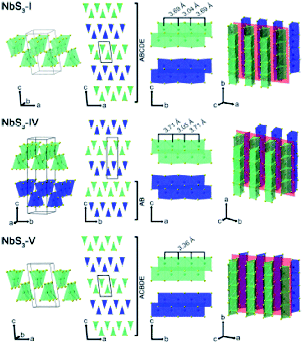 | ||
| Fig. 5 The crystal structure of NbS3-I, NbS3-IV, and NbS3-V: unit cells, chain cross-sections, layers, and perspective views. Reproduced with permission from ref. 55, copyright: 2017, Application Infrastructure Provider. | ||
In 1975, single-crystal NbSe3 was prepared by Meerschaut et al., and single-crystal XRD studies established the monoclinic structure, consisting of inestimable selenium trigonal prismatic chains loaded on top of each other with shared triangular faces.68–70 Similar to other MX3-based 2D materials, the structural arrangement with strong chemical bonding anisotropy makes NbSe3 crystals a tempting material with novel physical and chemical properties. The Se–Se bond lengths are testified to be 2.37 Å and 2.49 Å, respectively, with CDWs at 145 K and 59 K, and the Nb–Se bonds are strongly covalent–ionic in nature.70–73 From scanning tunnelling microscopy studies of NbSe3, it is clear that there are three distinguishable chains (I, II, and III) in the NbSe3 unit cell at all temperature.74 The III chains are identified by their association with the CDW modulation vector q1, and the two remaining chains are named I and II.
Among TaX3-based TMTCs, TaS3 and TaSe3 have been investigated due to their various fundamental microelectronic properties, which range from insulating to metallic conducting.65,75 TaS3 was first described by Blitz and Kocher in 1938 and later through XRD studies implemented by Jellinek in 1962.76,77 There are two commonly referenced structures of TaS3, a monoclinic state (m-TaS3) and an orthorhombic state (o-TaS3) (structure shown in Fig. 6a)104 (Table 1). Meerschaut et al. reported the complete structure of m-TaS3 with the space group P21/m, and the lattice constants are a = 9.515(2) Å, b = 3.3412(4) Å, c = 14.912(2) Å, and β = 109.99°.75 o-TaS3 forms in the space group C2221 and the lattice constants are a = 36.804 Å, b = 15.173 Å, and c = 3.340 Å.65,77 A high-pressure mhp-TaS3 phase with the identical space group to m-TaS3 has similar lattice parameters, expect there is a deviation of β by 3°.65 m-TaS3 is a low-dimensional conductor with inestimable chains of tantalum atoms along the b-axis of the primitive cell. The remarkable properties of bulk and few-layer TaS3 are directly correlated to the crystal structure, specifically the chains of tantalum atoms and the b-direction of the unit cell, which leads to quasi-1D properties. TaSe3 belongs to the V–X group of MX3 with a monoclinic crystal structure, in which the unit cell consists of stacks of Ta atoms, each of which are fused to three Se atoms above and below the b-axis.78,136 The monoclinic crystal structure of TaSe3 was first recorded by Bjerkelund and Kjekshus in 1965 with a = 10.402 Å, b = 3.495 Å, c = 9.829 Å, and β = 106.26°.79,80 The inter-planar distance (nearly 4 Å) is more than the distance between the Ta atoms (3.495 Å), which gives clear evidence for the quasi-1D properties of TaSe3.79
 | ||
| Fig. 6 (a) The orthorhombic structure of TaS3. (b and c) FESEM images of TaS3 nanobelts. (d) Temperature-dependent resistance changes of a single nanoribbon, with the inset showing a fabricated device. (e) Current–voltage curves and (f) differential conductance as a function of voltage measured at specific temperatures, with the inset of (f) showing the temperature dependence of the threshold voltage. Republished with permission from ref. 104, permission conveyed through Copyright Clearance Center, Inc. | ||
Monoclinic NbSe3 consists of three equidistantly placed metal chains with different (Se2)2− groups, and it is reported to show metallic conductivity with two charge density wave temperatures of 145 K and 59 K.69,87,88 Chaussy et al. reported two phase-transition temperatures of NbSe3 crystals at 145 K and 59 K based on electrical resistivity, magnetic susceptibility, and heat capacity measurements.87 As per their revisions, when the temperature decreased, the resistivity (ρ) decreased, showing the behaviour of a metal, and saturation was reached below 10 K. The maximum specific heat capacity was attained at 49 K and gradually decreased at T = 0 K. It was found to be diamagnetic at 4.2 K, and for fibres and powder samples of NbSe3, the magnetization values were equal to 1.35 × 10⁻⁷ emu g−1 (attributed to a parallel orientation to the magnetic field) and 5 × 10⁻⁷ emu g−1 (attributed to a random orientation to the magnetic field), respectively.87 Whiskers of NbSe3 and Fe-doped NbSe3 nanowires also showed two anomalies in resistivity that were adjunct to the CDW transitions at 140 K and 50 K.89 The successful doping of Fe atoms can be observed based on the strengthening of both the threshold fields, ET1 and ET2. Four-probe resistivity measurements of single-crystal NbSe3 nanowires showed the expected CDW transitions at T1 = 142 K and T2 = 58 K, and there was no magnetoresistance above the higher TCDW value and positive magnetoresistance below the lower TCDW value.72 Ido et al. explored the effects of pressure on CDW formation and superconductivity in NbSe3 via resistivity and diamagnetic measurements.90 It was observed that both the CDW transition temperatures T1 and T2 decreased steadily with an increase in pressure, while they later changed abruptly above 6 kbar pressure and tended to zero above Pc = 7.5 kbar (superconductivity appeared). The change in superconductivity arose from a clampdown on electron–phonon coupling.90 Latyshev et al. showed that the induction of oscillations into non-linear CDW conductivity could be attributed to columnar defects in NbSe3, which fluctuated with a magnetic field when the field was oriented parallel to the axes of the defects.73,91 Due to the CDW transitions, there were ample signs of electron–phonon scattering affecting the transport properties relating to the thermal conductivity of the lattice of NbSe3 nanowires.92 Ong et al. performed Hall measurements of NbSe3 and showed that at both TCDW values there is an increase in Hall resistivity (RH).93 But this was self-regulating below 3 K, and with an increase in the field value, it saturated at 2.3 × 10⁻⁶ m3 C−1. Surprisingly, the value of RH was 4.1 × 10⁻⁷ m3 C−1 at 2 K.93
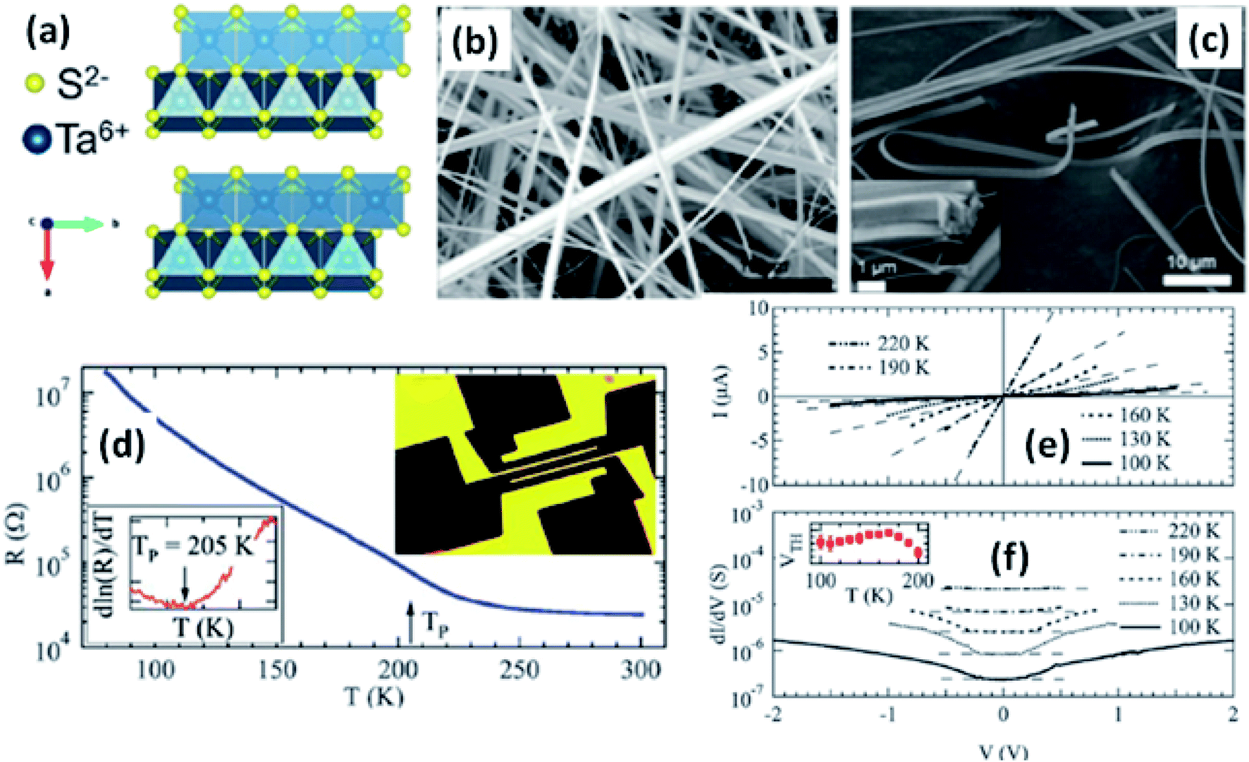
Resistivity measurements and electron diffraction studies of m-TaS3 and o-TaS3 showed two transition temperatures (240 K and 160 K), which were interpreted as succeeding Peierls transitions on the diverse chain types of TaS3.94 For o-TaS3, as the temperature dropped below the ambient temperature, the resistance gradually rose up to 230 K and then increased sharply. However, for m-TaS3, this happened in a typical manner, i.e., there was a sequential decrease and increase in resistance at 270, 220, and 180 K.94 The Peierls transition temperature, the temperature at which the slope of R vs. T attains its maximum, was also shown by Roucau et al. Peierls transitions in quasi-1D conductors are associated with intrinsic superstructures.94 Polarized Raman scattering studies of o-TaS3 demonstrated that at the Fermi surface, the formation of a CDW gap was held responsible for the reduction in free carriers.95 Thus, the scattering intensity decreased from interband processes along with an increase in the phonon energy. Nanosized TaS3 samples showed step-like conductivity as a function of strain, demonstrating the association of the steps with the quantization of the CDW wave vector.96 In o-TaS3, the asymmetrical conductivity had no dependency below a certain temperature (2 K), which was caused by soliton transport in the CDW system.97 Nichols et al. studied the frequency and voltage dependencies of voltage-induced torsional strain in o-TaS3 and concluded that the strain is allied with a divergence in the CDW instead of the CDW current.98 A change in the length, L, (depending on the electric field and time) of TaS3 samples demonstrated that hysteresis partly corresponds with resistance.99 Thermal expansion studies of o-TaS3 crystals showed the uncharacteristic behaviour of the hysteresis loop of length L below the Peierls transition temperature and at 100 K, the elastic modulus meets the Young's modulus of the CDW wave.100 Gorlova and co-workers observed electric-field-induced torsional strain corresponding to colossal shear in TaS3 whiskers.101 The threshold and hysteresis behaviour of torsion demonstrated its link with CDW deformation. Correspondingly, Nichols et al. investigated the effects of hysteretic voltage-induced torsional strain on CDW depinning in o-TaS3 using square-wave and triangular-wave voltages of dissimilar frequencies and amplitudes.102 Inagaki et al. reported the magnetoresistance of a CDW in o-TaS3 whiskers under a magnetic field up to 4.2 K. When the field was aligned with the a-axis, the maximum amplitude of angle-dependent magnetoresistance was achieved, whereas there was zero value at the b-axis.103 Electrical transport measurements of single o-TaS3 by Farley et al. discovered the depression of the Peierls transition temperature to 205 K. Below this temperature, there was depinning of the CDW, which was accredited to broadening of the electric field and surface confinement; low dimensionality and a limited size effect caused a great enhancement in the threshold voltage for the nucleation of CDW dislocations (Fig. 6).104 Wu et al. studied the pressure-dependent vibrational properties, which imply that the one and only S‖ mode (at 54 cm−1) was held accountable for the crystalline orientation of TaS3 through angle-resolved Raman spectroscopy and high-pressure diamond anvil cell studies.105 Frequency-dependent conductivity measurements showed the Drude type behaviour of the inertial feedback of TaS3, associated with damping.106
TaSe3 is reported to be superconducting below 2.1 K with anisotropic properties under the application of a magnetic field79 and Kikkawa et al. also indicated the superconductivity of TaSe3 at T = 1.9 K.65 Thickness-dependent work function variations of TaSe3 flakes confirmed the extended screening length (24 nm) at which the work function suddenly decreased, which specified its hydrophilic nature, and the Raman modes at 128 cm−1; 141, 164, 217, and 237 cm−1; 177 cm−1; and 186 cm−1 corresponded to Bg, B2, Ag, A1g modes, respectively.107 TaSe3 is reported to have a high current-carrying capacity and high current density, and it has emerged as a possible potential candidate to act as an interconnector in electronic devices due to capping with hexagonal boron nitride (h-BN).108 Experimental observations demonstrated that quasi-1D TaSe3 nanowires transmit lower levels of normalized noise spectral density, with potential for rationalized local interdependent applications.109–111 The main properties of MX3 are summed up in Fig. 7.
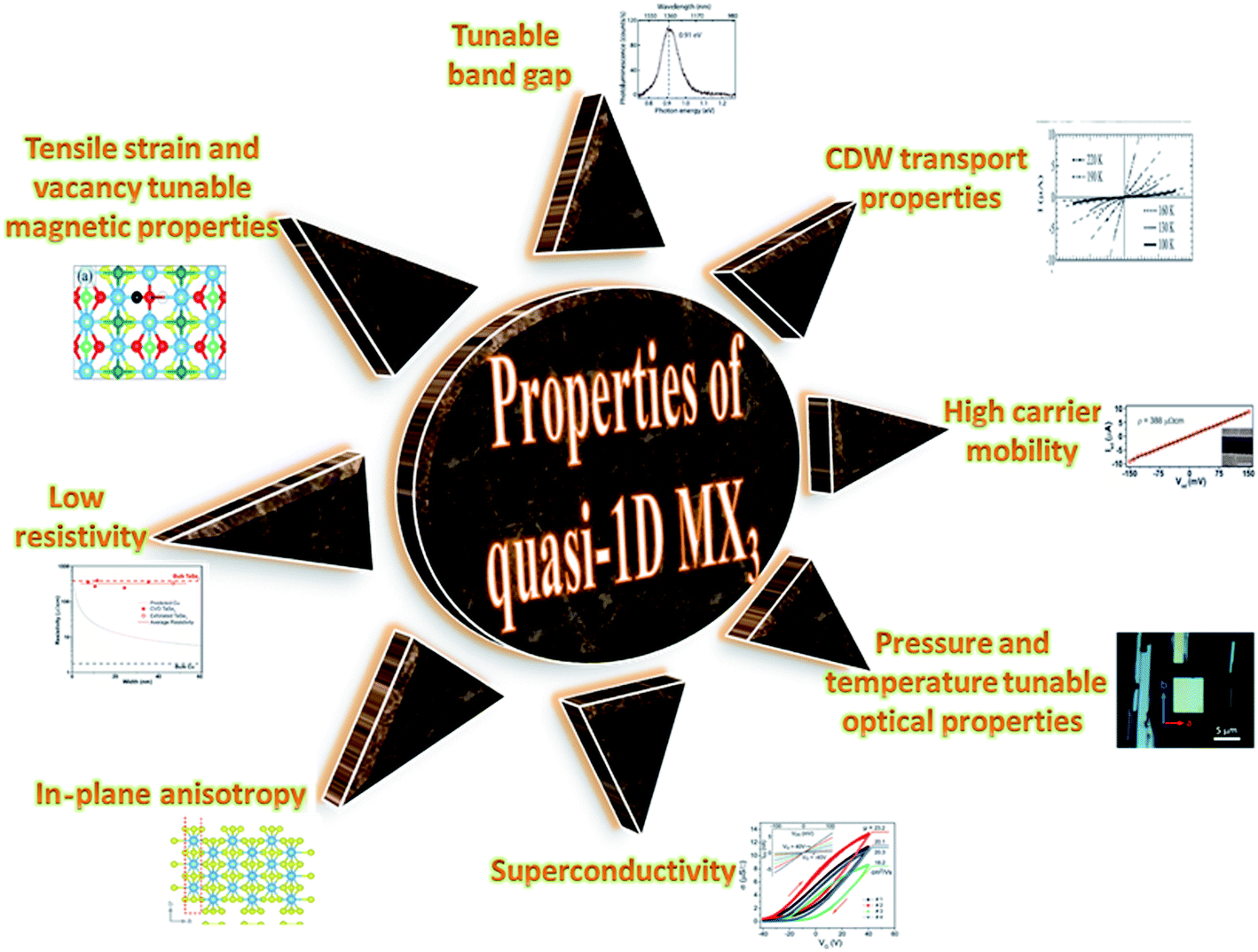 | ||
| Fig. 7 A schematic diagram showing the properties of quasi-1D MX3. Resistivity figure reprinted with permission from ref. 78, copyright: 2019, American Chemical Society; in-plane anisotropy figure republished with permission from ref. 9, permission conveyed through Copyright Clearance Center, Inc. (2016); superconductivity figure reproduced with permission from ref. 124, copyright: 2015, Royal Society of Chemistry; optical properties figure reproduced with permission from ref. 6, copyright: 2019, IOP Science; carrier mobility figure reprinted with permission from ref. 78, copyright: 2019, American Chemical Society; CDW properties figure republished with permission from ref. 104, permission conveyed through Copyright Clearance Center, Inc.; band gap figure reproduced with permission from ref. 6, copyright: 2019, IOP Science; magnetic properties figure reproduced with permission from ref. 9, copyright: 2015, American Chemical Society. | ||
3. Strategies for the growth of MX3
Synthesis approaches used for the growth of MX3 crystals and nanostructures such as nanowhiskers, nanoribbons, nanosheets, nanowires, etc. can be classified as top-down or bottom-up approaches. In this review, we have emphasized different synthesis approaches reported for MX3 development, as summarized in Table 3. Useful methods for MX3 include direct chemical reactions, chemical vapour transport (CVT), chemical vapour deposition (CVD), high-pressure evolution approaches, intercalation, mechanical and chemical exfoliation, etc. Characterization techniques such as X-ray diffraction (XRD), X-ray photoelectron spectroscopy (XPS), field-emission scanning electron microscopy (FESEM), atomic force microscopy (AFM), scanning tunnelling microscopy (STM), transmission electron microscopy (TEM), Raman spectroscopy, UV spectroscopy, and optical microscopy (angle-resolved as well as pressure- and temperature-dependent methods) are the usual procedures used to estimate the properties of MX3 materials and further help in exploring their abundant applications.112–120| Material | Starting precursors | Growth conditions | Heating temperature; substrate | Size | Ref. no. |
|---|---|---|---|---|---|
| TiS3 crystals | Ti sheets, S powder | Vacuum-sealed (10−6 torr) ampoule, 5 days | 520 °C; wall of quartz tube | Bulk crystals | 24 |
| TiS3 thin film | TiCl4, t-butyl disulfide | Vacuum heating (10−1 torr) | 260 °C; glass, and Ti and Al foil | Large-area thin film | 127 |
| TiS3 nanowhiskers | Ti metal foil, S powder | Vacuum-sealed (10−5 torr) ampoule, 3 days | 500 °C; Ti foil and wall of quartz ampoule | l = 100 μm, w = few μm, t = 0.5 μm | 28 and 124 |
| TiS3 nanoribbons | Ti disc, S powder | Vacuum-sealed (10−3 torr) ampoule, 20 h | 520 °C; wall of quartz tube | l = 100 μm, w = 1–5 μm, t = 5–200 nm | 144 |
| ZrS3 flakes | Zr metal sheets, S pellet | Vacuum-sealed (10−6 torr) ampoule, 5 days | 650 °C; wall of quartz tube | Bulk needles and mechanically exfoliated flakes | 25 and 144 |
| ZrSe3 crystals and nanobelts | Zr powder, Se powder | Vacuum-sealed (10−2 torr) ampoule, 24 h | 650 °C; wall of quartz tube | l = tens of μm, w = 20–2600 nm | 129 |
| ZrTe3 crystals | Zr powder, Te powder | Vacuum-sealed ampoule | 950 °C (source)/850 °C (sink) and 735 °C (source)/660 °C (sink); wall of quartz tube | l = 5 mm, w = 0.8 mm, t = 0.2 mm | 15 |
| HfS3 crystals and flakes | Zr metal sheets, S pellet | Vacuum-sealed (10−6 torr) ampoule, 5 days | 650 °C; wall of quartz tube | Bulk needles and mechanically exfoliated flakes | 24 |
| HfSe3 crystals and flakes | Hf powder, Se powder | Vacuum-sealed (10−2 torr) ampoule, 24 h | 650 °C; wall of quartz tube | l = tens of μm, w = 20–2600 nm | 129 |
| HfTe3 crystals and flakes | Hf powder, Te powder | Vacuum-sealed, CVT-iodine carrier | 500–540 °C; wall of quartz tube | l = 0.3 mm, w = 0.3 mm, t = 0.1 mm | 51 |
| NbS3 whiskers and flakes | Nb powder, S powder | Vacuum sealed (10−5 torr) ampoule, 7 days | 550 °C (source)/470 °C (sink); wall of quartz tube, mechanical exfoliation | Whisker-like crystals | 84 |
| NbSe3 crystals | Nb powder, Se powder | Reaction under vacuum, 15 days | 700 °C; wall of quartz tube | l = 7.0 mm, w = 0.05 mm, t = 0.01 mm | 87 |
| NbSe3 nanoribbons | Nb powder, Se powder | Reaction under vacuum, >15 days | 700 °C; wall of quartz tube | l = >10 μm to few mm, w = t = 20–700 mm | 72 |
| TaS3 crystals and flakes | Ta powder, S powder | Vacuum sealed, CVT-iodine carrier, 48 h | 760 °C; wall of quartz tube | l = several cm, w = 40–900 nm, t = 20–50 mm | 132 |
| TaSe3 crystals and flakes | Ta powder, Se powder | Vacuum sealed, CVT-iodine carrier, 10 days | 700–600 °C; wall of quartz tube | l = >10 mm, w = t = ∼200 μm | 107 and 108 |
| TaSe3 nanowires | TaCl5, Se powder | CVD growth under vacuum, Ar + H2 gas, 15 min | 400 °C; wall of quartz tube and substrate | l = >120 nm | 78 |
3.1. Bottom-up approaches
![[thin space (1/6-em)]](https://www.rsc.org/images/entities/char_2009.gif) :3).129 The powder mixture was vacuum sealed (10−2 Pa) in a quartz tube and heated at 650 °C for 24 h to achieve the growth of ZrSe3 and HfSe3 nanobelts. ZrTe3 nanoribbons could be grown via a CVD approach, in which Te and ZrCl4 powder are used as vapour sources (Fig. 8e and f).130 Through controlling the carrier gas flow (Ar: 30 sccm and H2: 35 sccm), heating temperature (650–750 °C), and growth time (20–80 min), high-quality and single-crystal nanoribbons could be grown on a SiO2/Si substrate placed downstream of the quartz tube.130
:3).129 The powder mixture was vacuum sealed (10−2 Pa) in a quartz tube and heated at 650 °C for 24 h to achieve the growth of ZrSe3 and HfSe3 nanobelts. ZrTe3 nanoribbons could be grown via a CVD approach, in which Te and ZrCl4 powder are used as vapour sources (Fig. 8e and f).130 Through controlling the carrier gas flow (Ar: 30 sccm and H2: 35 sccm), heating temperature (650–750 °C), and growth time (20–80 min), high-quality and single-crystal nanoribbons could be grown on a SiO2/Si substrate placed downstream of the quartz tube.130
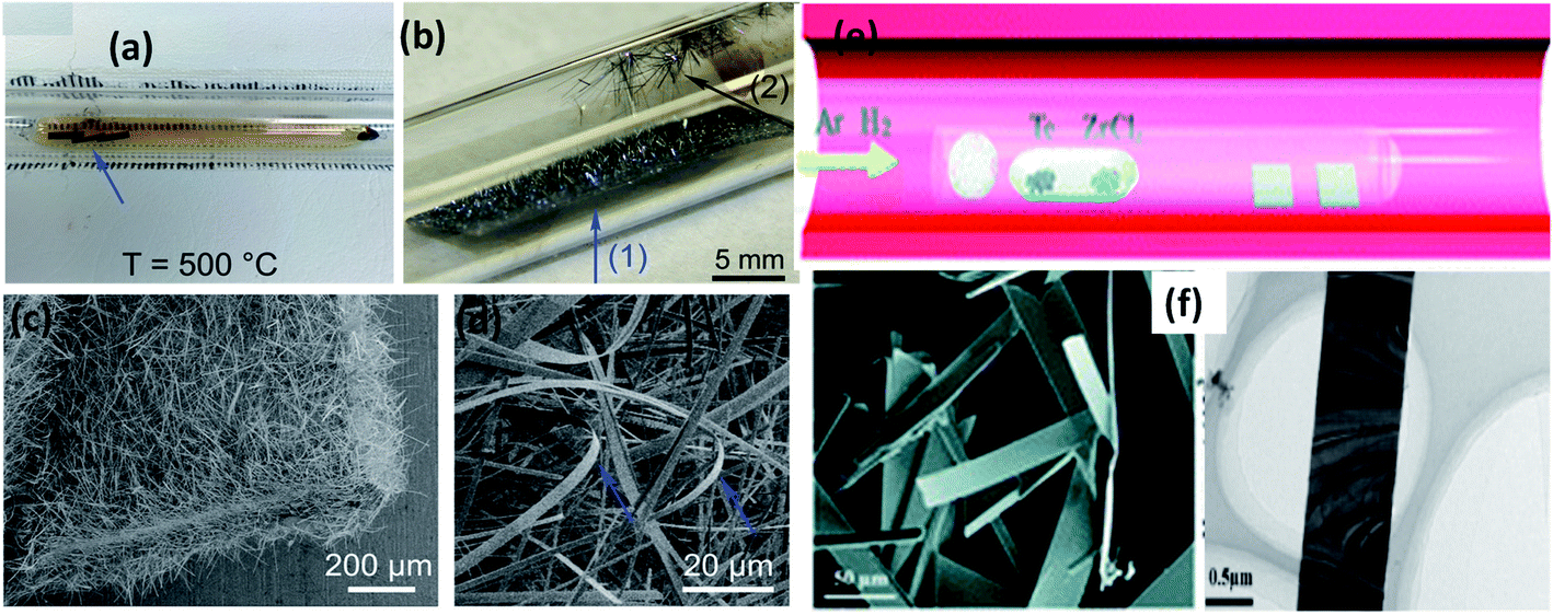 | ||
| Fig. 8 The synthesis of MX3. Optical photographs of the ampoule (a) before and (b) after the growth of TiS3 whiskers on Ti foil and the surface of quartz. (c and d) SEM images of the grown TiS3 whiskers with arrow marks indicating samples collected from the respective positions. Reproduced with permission from ref. 124, copyright: 2015, Royal Society of Chemistry. (e) The synthesis of ZrTe3 via a chemical vapour deposition approach. (f) FESEM and TEM images of ZrTe3. Republished with permission from ref. 130, permission conveyed through Copyright Clearance Center, Inc. | ||
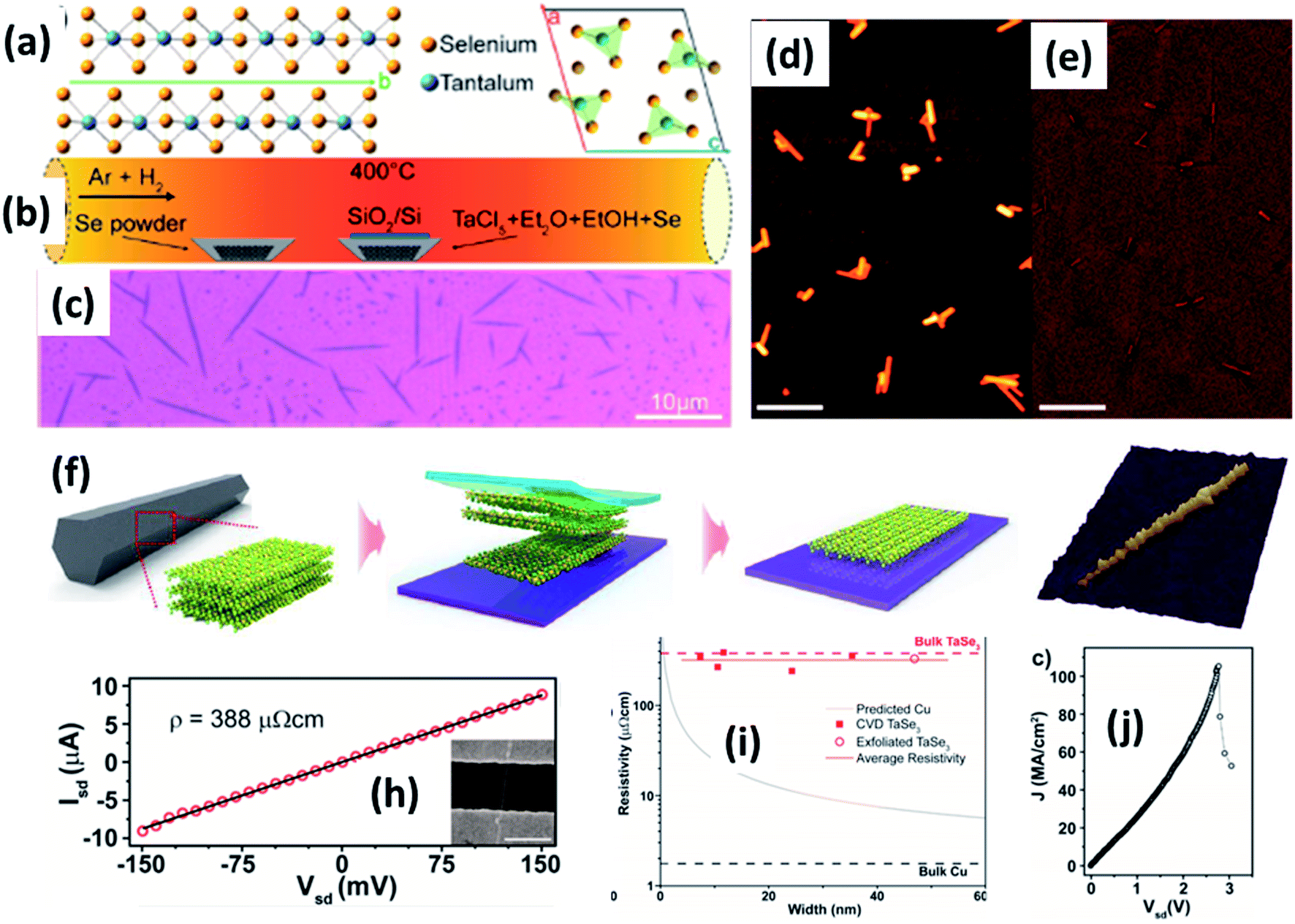 | ||
| Fig. 9 (a) The crystallographic structure of TaSe3. (b) A schematic diagram of the CVD set-up for the growth of TaSe3 nanowires. (c) An optical image and (d and e) SEM images of a population of TaSe3 nanowires. Reprinted with permission from ref. 78, copyright: 2019, American Chemical Society. (f) A schematic illustration of the mechanical exfoliation of TaSe3 flakes from bulk TaSe3. (g) A 3D representation of a quasi-1D TaSe3 nanoribbon monolayer on a SiO2/Si substrate. Reproduced with permission from ref. 107, copyright: 2019, Multidisciplinary Digital Publishing Institute. (h) Source-drain current vs. voltage for a 11.6 nm TaSe3 nanowire in a 2-electrode configuration, with the inset showing an SEM image of the device. (i) Resistivity as a function of bundle width of CVD-grown TaSe3 nanowires and a comparison with bulk Cu and exfoliated TaSe3. (j) The current density response of a 7 × 7 nm2 nanowire as a function of Vds with failure at a current density of 108 A cm−2. Reprinted with permission from ref. 78, copyright: 2019, American Chemical Society. | ||
3.2. Top-down approaches
Chemical and mechanical exfoliation methods are widespread synthesis tactics that have gained huge interest in the field of top-down approaches.137,138 Mostly, as-prepared bulk crystals are taken as a prime precursor and subsequent chemical intercalation or power-driven force approaches are applied to these. Then, through force or intercalation, the neighbouring layers get detached from adjacent layers. Weak van der Waals forces co-existing between neighbouring layers plays a vibrant role in the materialization of few- to mono-layer crystals of 2D materials upon controlling the relevant parameters. Similarly, the ultrasonication of bulk powder or crystals in solvents is widely used for liquid exfoliation to achieve single- to few-layered nanosheets.Mechanical exfoliation is a widely used method to isolate single- to few-layered MX3 nanosheets from bulk material.6 On the other hand, liquid phase exfoliation is an effective method for the large-scale production of MX3 nanosheets.139 Few-layer TiS3 material was prepared by Island et al. at a temperature of 400 °C with sheet-like morphology, and this was later mechanically exfoliated to few-layer form.6 Xie et al. reported the liquid phase exfoliation of bulk ZrS3 in n-propylamine for 30 min followed by heating at 120 °C for 3 days in a Teflon-lined autoclave.139 The obtained product was washed and ultrasonicated in 1-cyclohexyl-2-pyrrolidinone to achieve ZrS3 nanosheets. NbS3 and NbSe3 nanoparticle colloidal solutions were prepared via a top-down approach through the ultrasonication of powder in different solutions (DMF, acetone, acetonitrile, ethanol, a water–ethanol mixture, etc.) for 3 h. Li-ion intercalation is proposed as a suitable method to prepare MX3 nanoribbons, in which three lithium atoms are incorporated into an MX3 unit to yield Li3MX3.140 A mechanical exfoliation approach is employed to prepare few-layered flakes from TaSe3 crystals (Fig. 9f and g).107 A schematic diagram of the different steps used in this process is shown in Fig. 9, in which wafer dicing tape is used and stuck onto the crystal, which is then removed and adhered to the SiO2/Si substrate.
4. Advanced applications of MX3
4.1. FETs
The possible applications of TMTCs are shown in Fig. 10. Due to the direct optical band gap (∼1 eV) and ultra-high response of TiS3, it has been used as an appropriate material for field-effect transistors with high gain.125,126 FETs based on 2D sheets of TiS3 whiskers (mechanically exfoliated few-layered samples) have been fabricated on SiO2/Si substrates (Fig. 11a and b).124 n-Type electronic transport TiS3-based FETs exhibited mobilities of 18–24 cm2 V−1 s−1, and this was improved to 43 cm2 V−1 s−1 upon the addition of another substrate, i.e., Al2O3, through a conventional atomic layer deposition (ALD) procedure. Similarly, the ON/OFF ratio improved to 7000 from 300 upon the use of Al2O3 as an alternative substrate (Fig. 11c).124 The temperature-dependent transfer curves of TiS3 nanowire FETs showed a metal–insulator transition, with a cross-over temperature of 220 K and mobility of 20–30 cm2 V−1 s−1.141 To demonstrate the anisotropic electrical properties, a TiS3 nanosheet FET device was made up, with electrodes at 30° intervals.126 The fabricated FET device worked along the b-axis of the TiS3 nanosheets, which was determined via computing the transfer characteristics across the device between two opposite electrodes at variable angles. A polar plot of current vs. voltage showed the high mobility of 80 cm2 V−1 s−1 (b-axis) and low mobility of 40 cm2 V−1 s−1 (a-axis) of the nanosheets. Transfer characteristics curves showed n-type behaviour, with an ON/OFF ratio of five.126 The nanoribbons showed lower mobilities with advanced electric field and optical properties, which later can be tuneable. The multifaceted concentration of sulphur vacancies in samples grown at lower temperature played an important role in creating tuneable properties upon an intensification in the n-type dopant.126 The interfacial and contact properties of multi-layered TiS3 and metals (Au, Ag, Pd, Pt, Ir, and Ni) have been inspected via DFT and the outcomes suggested the absence of tunnelling barriers, demonstrating superior carrier injection abilities from the metal to multilayer TiS3 in FET and other electrical devices.142 The output characteristics of FETs based on HfS3 nanobelts confirmed the p-type semiconducting nature.142 Therefore, from the above data, it is quite evident that these materials are first and foremost highly suitable materials for nanoelectronics and optoelectronic devices.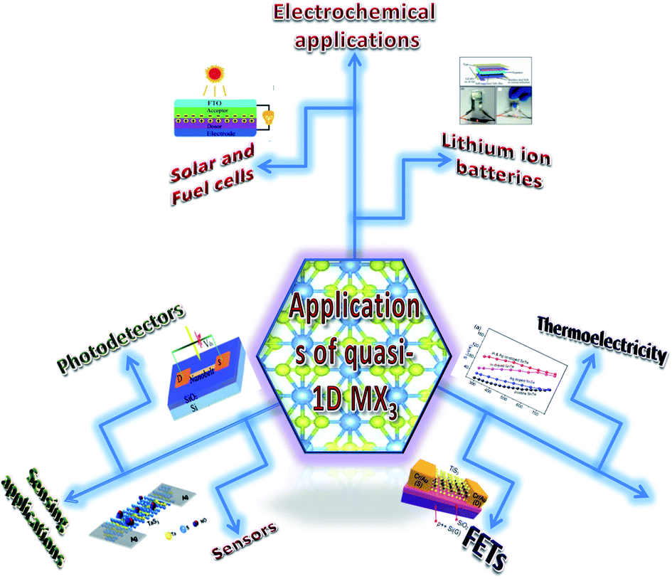 | ||
| Fig. 10 A schematic diagram showing the various applications of MX3. Solar and fuel cell figure republished with permission from ref. 33, permission conveyed through Copyright Clearance Center, Inc.; lithium-ion batteries figure reprinted with permission from ref. 134, copyright: 2015, American Chemical Society; sensors figure reprinted with permission from ref. 133, copyright: 2018, American Chemical Society; photodetectors figure republished with permission from ref. 129, permission conveyed through Copyright Clearance Center, Inc.; FETs figure reproduced with permission from ref. 124, copyright: 2015, Royal Society of Chemistry; thermoelectricity figure republished with permission from ref. 157, permission conveyed through Copyright Clearance Center, Inc.; central figure reproduced with permission from ref. 6, copyright: 2015, Springer Nature. | ||
 | ||
| Fig. 11 Few-layered TiS3 FETs. (a) A schematic diagram and (b) an SEM image of a typical FET. (c) Conductivity vs. gate voltage dependencies of four different fabricated FETs, with the inset showing drain source current vs. drain source voltage at different gate voltages. Reproduced with permission from ref. 124, copyright: 2015, Royal Society of Chemistry. | ||
4.2. Solar and fuel cell devices
Solar water splitting using photoelectrochemical cells is an effective and efficient way of storing solar energy in the form of hydrogen, which can be used as a fuel. For hydrogen generation via water splitting, the light absorbing material with appropriate energy band positions, i.e., the energy band levels (CB and VB), should be suitable with respect to the water reduction potential.143,163 Anisotropic MX3 materials possess the advantages of having a low band gap to absorb direct solar energy and being widely available, non-toxic, and suitable for photoelectrochemical water splitting. Fig. 12a144 shows an SEM image of TiS3 nanoribbons, which have been employed as an active material for electrochemical water splitting.144 The systematic energy level band diagram of TiS3/electrolyte (Na2SO3) is shown in Fig. 12b144 with a flat band potential (Vfb) at −0.48 VNHE, and this is used to calculate the semiconductor Fermi level. The conduction and valence band energy levels in terms of potential and energy balance, along with the redox potentials for the water splitting half reactions at pH = 9, are shown in the band diagram. Hydrogen evolution occurs on the TiS3 nanoribbons at 0 V and investigations at different bias potentials yielded a photoconversion efficiency of about 7% at a bias potential of 0.3 V (Fig. 12c and d).144 In another work, Flores et al. demonstrated the energy level schemes for an MX3/electrolyte interface, and comparable photogenerated hydrogen fluxes are reported for TiS3, ZrS3, and HfS3.145 A TiS3 photoanode is reported to generate up to 19 nmol H2 per min per cm2 at an external bias potential of 0.3 V vs. Ag/AgCl. Due to the presence of copious amounts of Se2 bonds on the surface of the ZrS3 ultrathin nanosheets, enhanced oxygen evolution reaction performance was observed compared to the bulk counterpart.139 A low onset overpotential of 244 mV and Tafel slope of 45 mV per decade are achieved using ZrS3 nanosheets in strongly alkaline solution (pH = 14), whereas in weakly alkaline solution (pH = 6.9), the onset over-potential and Tafel slope are reported to be lower.139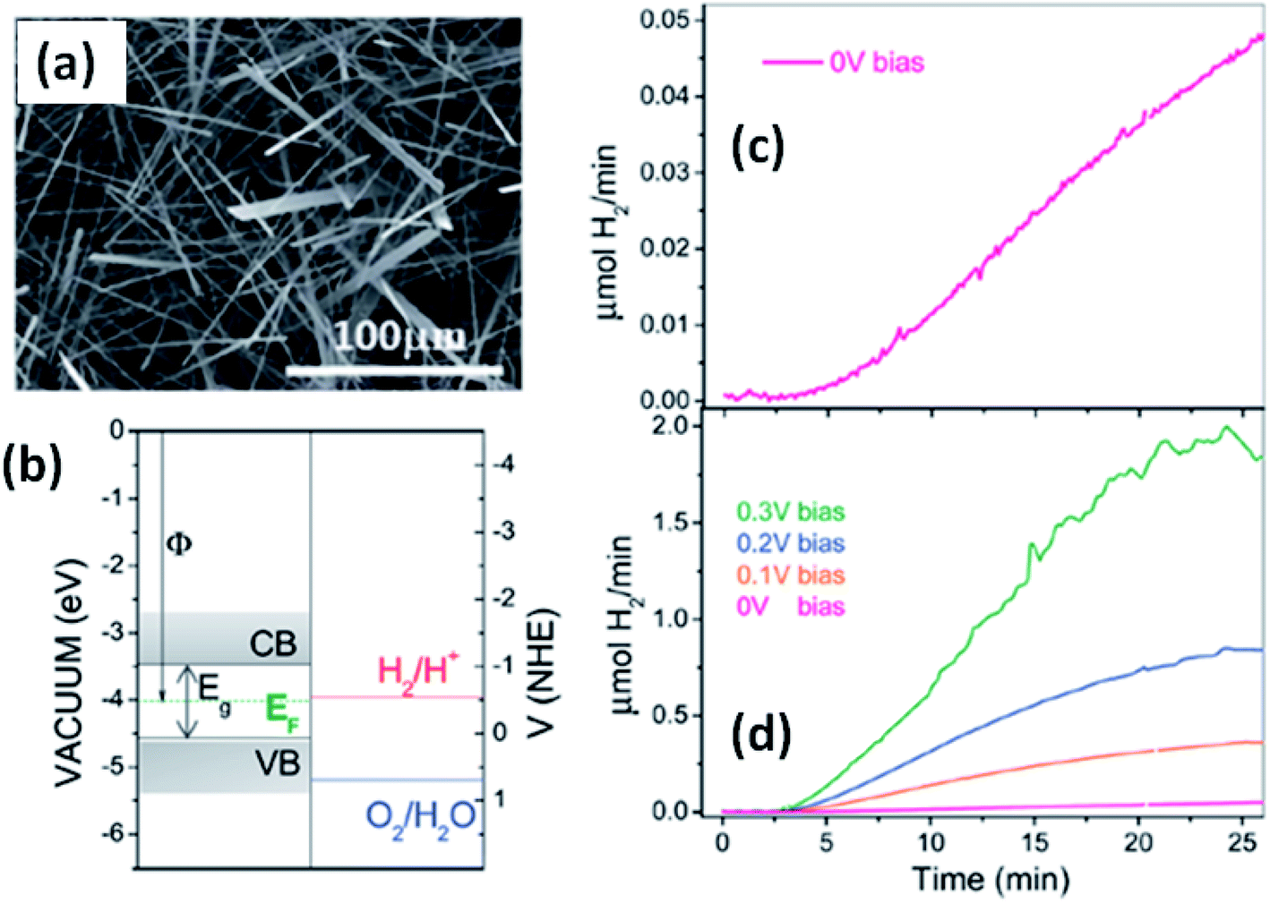 | ||
| Fig. 12 The hydrogen photogeneration properties of MX3 nanostructures. (a) An SEM image and (b) the conduction and valence band energy levels on potential (V vs. NHE) and energy (eV vs. vacuum) scales, with the redox potentials for the water-splitting half reactions at pH = 9.0 vs. NHE, of TiS3 nanoribbons. The hydrogen evolution flow of TiS3 nanoribbons (c) at 0.0 V and (d) at different bias potentials. Republished with permission from ref. 144, permission conveyed through Copyright Clearance Center, Inc. | ||
The use of 2D materials and their heterojunctions in optoelectronics and solar-correlated devices is utterly controlled by the superiority of the heterojunction formed and the band alignment to tune carriers at interfaces.33 Zhao et al. employed DFT to calculate the band superstructures and heterostructures of IV–VIA monolayers of MX3 (M = Zr, Hf; X= S, Se) and VIIB–VIA monolayer MX2 (M = Tc, Re; X = S, Se). The calculations indicated that for MX3, the valence bands are dependent on the p-states of chalcogens, whereas the d-states of the transition metals control the conduction bands. For MX2 monolayers, both the valence and conduction bands depend on the d-states of the transition metals. Considering standard water redox potentials (−4.44 eV and −5.67 eV for reduction (H+/H2) and oxidation (O2/H2O), respectively), the combination of MX3 and MX2 monolayers and their band alignment to create efficient heterostructures have been reported.33 Fig. 1333 shows the band-offset components and a contour map of power conversion efficiency (PCE) values. From calculations, it is predicted that a ZrS3/HfS3 bilayer thin-film device could achieve 16–18% efficiency, which is much higher than other reported 2D heterojunction solar cell devices. Similarly, Ahammed et al. reported that the PCEs in ZrS3/MoS2, ZrS3/WS2, ZrS3/MoSeTe, ZrS3/WSTe, and ZrS3/WSeTe heterostructured bilayers are as high as ∼12%, 8%, 16%, 14%, and 14%, respectively.146 Recently, anisotropic ZrS3 has been reported to act as an active material for perovskite light-emitting diodes and P–N junction diodes, and the results are found to be promising, which opens up pathways for further research into the area of MX3 heterojunctions for optoelectronics and solar-cell devices.147,148
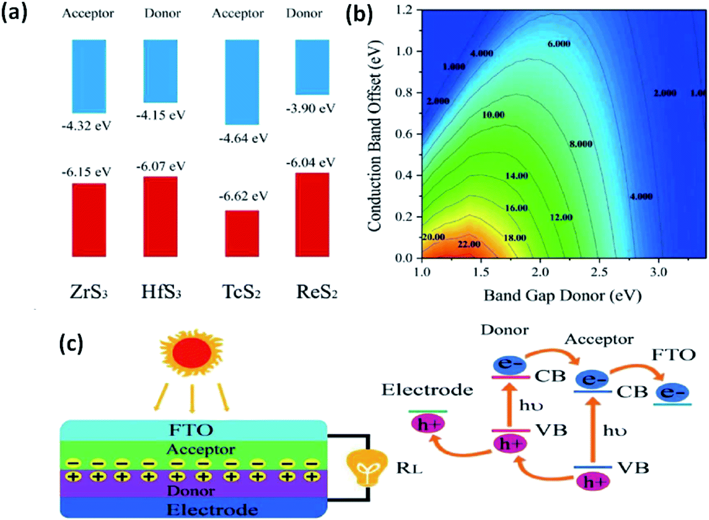 | ||
| Fig. 13 The application of MX3 heterostructures to solar cells. (a) Band offsets of ZrS3/HfS3 and TcS2/ReS2 with the vacuum level as zero reference. (b) PCE contours obtained as a function of the donor band gap and conduction band offset. (c) A schematic illustration of thin-film solar cells with the associated mechanism. Republished with permission from ref. 33, permission conveyed through Copyright Clearance Center, Inc. | ||
4.3. Photodetectors and sensors
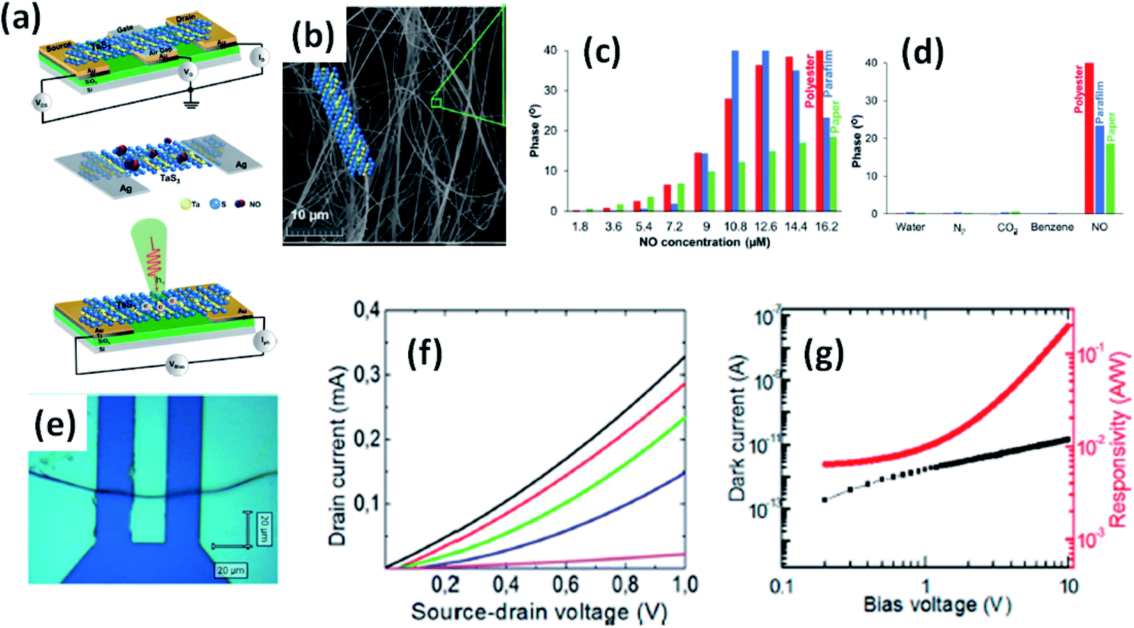
Island et al. reported the photoresponse properties of TiS3-nanoribbon-based FETs.125 TiS3 FETs showed a high photoresponse of up to 2910 A W−1, and fast switching times of ∼4 ms, with a cut-off frequency of 100 Hz, showing promise for photodetection and photovoltaic applications. Tao et al. reported flexible a visible light photodetector formed on ZrS3 nanobelt film, which showed high spectral selectivity, a wide range, and a rapid photoresponse in the visible light to near-infrared region.149 Photodetectors based on HfS3 FETs showed a huge ON/OFF ratio of 337.5, along with an ultralow dark current of 0.04 pA at 405 nm under 1.2 mW cm−2 light excitation.32,142 CVT-deposited ZrSe3 and HfSe3 were investigated for photodetection applications.129 Under excitation by 650 nm wavelength light, a ZrSe3 photodetector showed a light ON/OFF ratio of 1.92 at 50 s with a bias voltage of 5 V (Fig. 14).129 Similarly, a HfSe3 nanobelt photodetector showed an ON/OFF ratio of 2.2 with an average time of 50 s, and the photoresponse time was 0.4 s. Although HfTe3-based materials are reported to show interesting properties, including CDWs, superconductivity, and the ability to be used in quantum Hall-effect-related devices, they have been less studied to date.51,150 Wu et al. reported a photothermoelectric (PTE) detector based on NbS3 with considerable performance in the UV to terahertz range.150 Considering its immense surface-to-volume ratio and reduced magnitude, mechanically exfoliated quasi-1D NbS3 crystals prepared via a CVT approach were studied for photodetector applications (Fig. 15a–d).151 Various types of continuous-wave lasers were used to test the photoresponse performance, including UV (375 nm), near-infrared (NIR, 1064 and 1550 nm), visible (635 nm), and semiconductor lasers, a mid-infrared (MIR, 10.6 μm) CO2 laser, and a terahertz-wave-generating far-infrared gas laser (118.8 μm) (Fig. 15e).151 The photodetector based on NbS3 flakes showed good performance, with responsivities higher than 1 V W−1, a response time of ∼7 ms, and robust flexibility and stability (Fig. 15e–g).151 Via employing the interesting structural and attractive electronic properties of layered TaS3 prepared in the form of nanofibers, Pumera and co-workers reported a highly selective impedimetric NO gas sensor, FET and photodetector (Fig. 16).133 The nanofibers showed metallic character, with a metal-semiconducting transition below 210 K, prompted by CDW formation. The impedimetric gas sensor showed an excellent response towards NO when fabricated on different substrates (Fig. 16).133 A TaS3-based sensor fabricated on a polyester substrate showed the best sensing performance, with a limit of detection (LOD) of 0.48 ppb.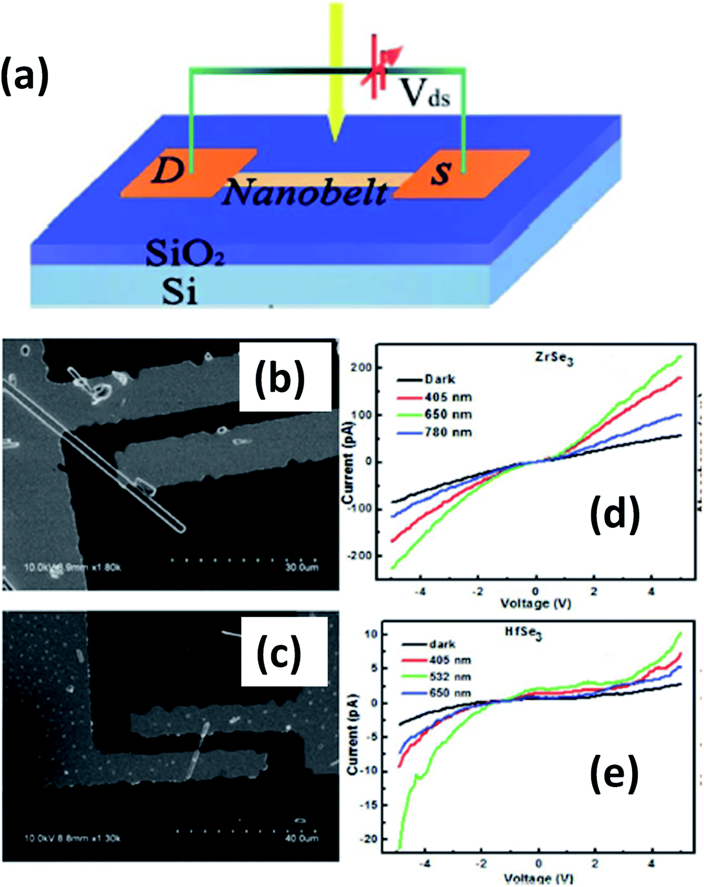 | ||
| Fig. 14 (a) A schematic illustration of a ZrSe3 and HfSe3 single nanobelt photodetector. SEM images of (b) ZrSe3 and (c) the HfSe3 photodetector. I–V characteristics of (d) ZrSe3 and (e) the HfSe3 nanobelt photodetector. Republished with permission from ref. 129, permission conveyed through Copyright Clearance Center, Inc. | ||
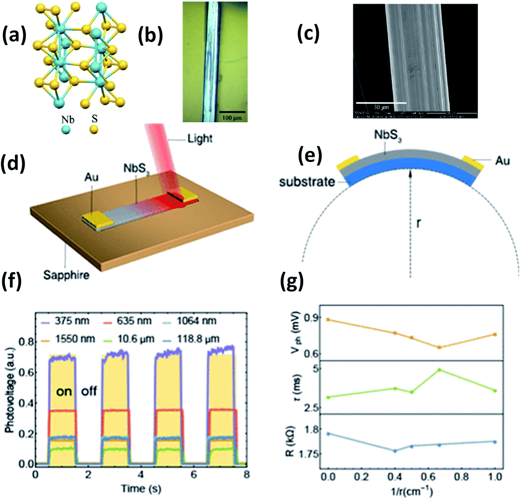 | ||
| Fig. 15 (a) The crystal structure of NbS3. (b) Optical microscopy and (c) SEM images of a NbS3 crystal. Schematic diagrams of (d) a NbS3 photodetector and (e) bending conditions. (f) ON–OFF photovoltage curves at room temperature and (g) resistance, response time, and photovoltage data under different bending conditions. Reprinted with permission from ref. 151, copyright: 2020, American Chemical Society. | ||
 | ||
| Fig. 16 (a) Schematic representations of a FET, NO gas sensor, and photodetector based on TaS3 nanofibers. (b) An SEM image of the TaS3 nanofibers. (c) The impedance phase responses of gas sensors fabricated on different substrates (polyester, parafilm, paper) as functions of NO concentrations. (d) Selectivity studies of the sensors fabricated on different substrates. (e) An optical image of a FET based on TaS3 fibers. (f) FET transistor characteristic curves at different gate voltages (pink: −1 V, blue: 0 V, green: 1 V, red: 2 V, black: 3 V). (g) Dark current (black) and responsivity (red) curves. Reprinted with permission from ref. 133, copyright: 2018, American Chemical Society. | ||
4.4. Lithium ion batteries
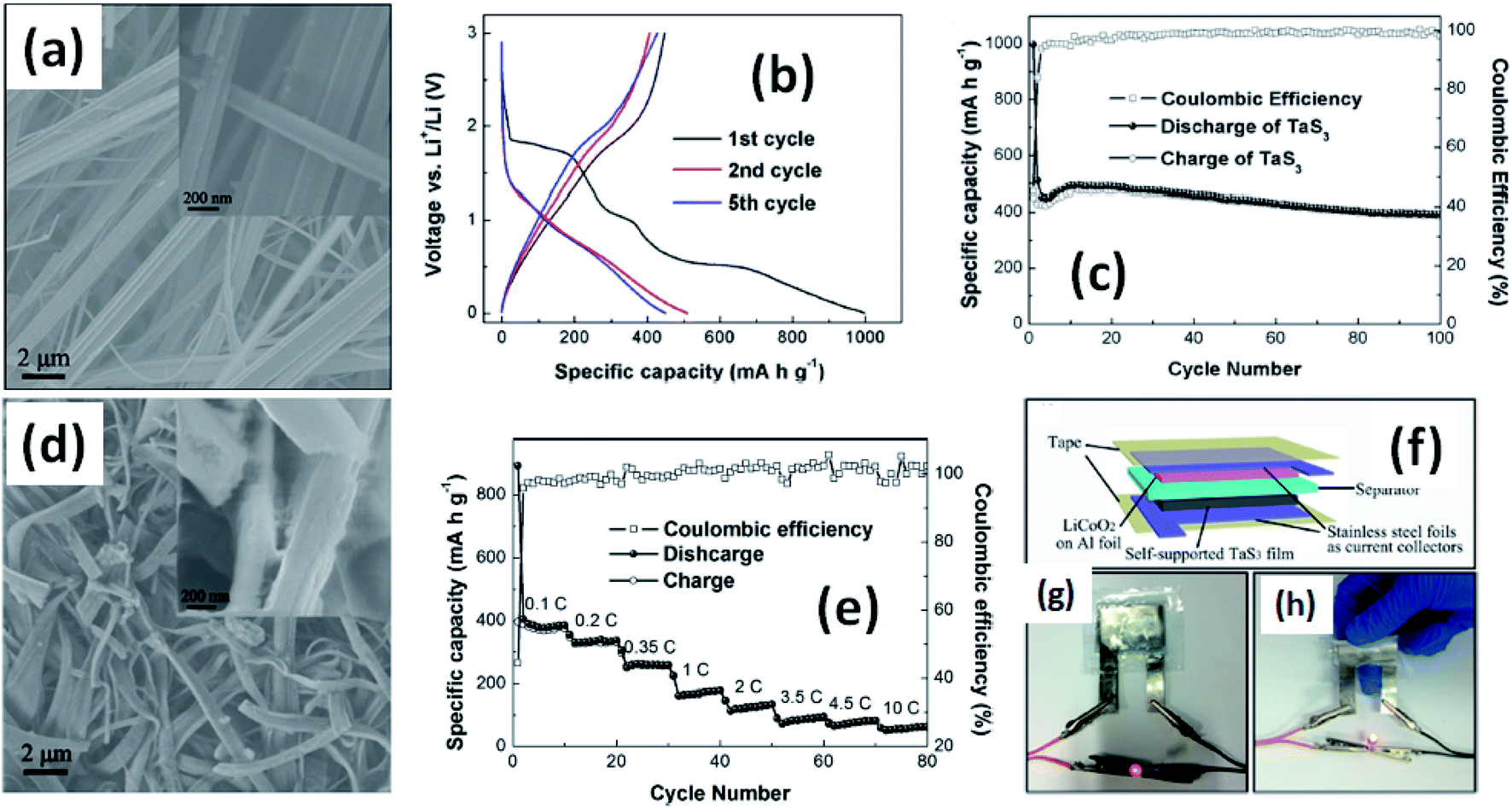
Due to their multi-electron processes with high theoretical capacity, MX3-based materials have emerged as potential active materials for lithium- and sodium-ion battery applications.152–155 Wu et al. investigated Li/Na adsorption and diffusion in bulk, few-layer, and monolayer TiS3 via studying the phase stability, electron properties, adsorption and dispersion properties, capacity, and plateaus. Charge density and Bader charge analysis studies provided information about the interactions of Li/Na with nearby atoms.152 The above-mentioned analysis methods also confirmed significant charge transfer from Li or Na atoms to surrounding sulphur atoms, and this effect was prominent in monolayer TiS3. Amorphous TiS3, prepared via the ball milling of TiS2 and S, is testified to show a capacity of 400 mA h g−1 when used as a Li-ion battery electrode material.153 Tanibata et al. reported an all-solid-state sodium cell using TiS3 as the active material, which showed a capacity of over 300 mA h g−1 during the first charge–discharge process.154 The capacity of a cell with a TiS3 electrode is reported to be three times higher than that of a cell with TiS2 crystals. Ex situ characterization (XRD and Raman spectroscopy) studies of the electrode materials after long-term cycling tests confirmed that TiS3 maintained its amorphous nature and local structure. Considering the advantages of its metallic nature and the high surface area of NbSe3, Li et al. demonstrated its application as an anode material in lithium-ion batteries.155 Pure and NbSe3 nanobelts wrapped with reduced graphene oxide (rGO) were prepared via a chemical approach (Fig. 17a–c).155 The wrapped rGO utilized strain from NbSe3 structural distortion to suppress impairment induced by volume alterations in the structure of NbSe3 nanobelts during charge–discharge cycles (Fig. 17g).155 NbSe3@rGO showed a discharge capacity of 300 mA h g−1 after 250 cycles at a current density of 100 mA g−1, which was four times greater than that of untainted NbSe3 nanobelts. Li et al. demonstrated self-supported and flexible lithium ion battery anode electrodes based on TaS3 nanowires with a good reversible capacity of ∼400 mA h g−1 after 100 cycles at 0.1C with 0.1% decay (Fig. 18).134 Due to the continuous and interconnected nature of the TaS3 nanowires, binder-free and self-supported electrodes could be fabricated, which not only enabled fast electron and ion access but also provided high mechanical flexibility in the fabricated cells.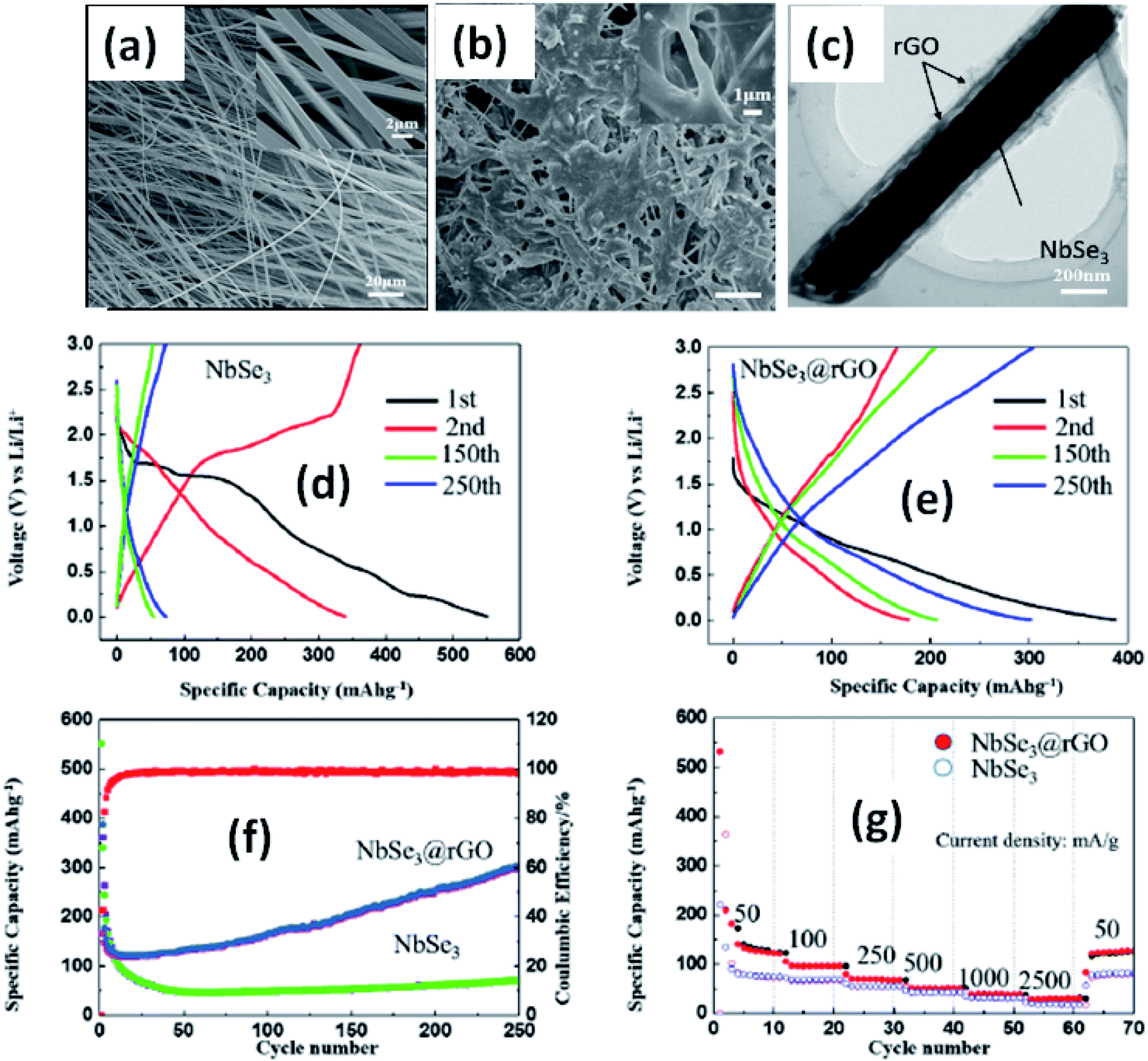 | ||
| Fig. 17 SEM images of (a) NbSe3 and (b) NbSe3@rGO. (c) A TEM image of NbSe3@rGO. The electrochemical performance of NbSe3 and NbSe3@rGO in the voltage range of 0.005–3 V vs. Li/Li+. Discharge and charge curves of (d) NbSe3 and (e) nanobelts. (f) The cycling performance of NbSe3@rGO and NbSe3 nanobelts at a current density of 100 mA g−1. (g) The rate performances of NbSe3@rGO and NbSe3 nanobelts. Reprinted from ref. 155, copyright: 2017, with permission from Elsevier. | ||
 | ||
| Fig. 18 (a) An SEM image of TaS3 nanowires. (b) Voltage profiles of a lithium-ion battery based on TaS3 nanowires cycled between 0.001 and 3 V vs. Li+/Li at a cycling rate of 0.1C. (c) Capacity and coulombic efficiency as a function of cycle number for a TaS3 nanowire electrode at a cycling rate of 0.1C. (d) An SEM image of nanowires after long-term cycling tests. (e) Rate performance and coulombic efficiency as a function of cycle number for TaS3 electrodes and as a function of discharge rate (0.1–10C). (f–h) A schematic diagram of a fabricated flexible lithium-ion battery with photographs showing a glowing LED powered by flat and bent states. Reprinted with permission from ref. 134, copyright: 2015, American Chemical Society. | ||
4.5. Thermoelectricity
The thermoelectric effect is mainly a translation between temperature gradients in a material and electronic voltage, and it also works contrariwise. Thermoelectric constituents convert heat into electric power and they have been used to design eco-friendly and sustainable energy sources.156,157 The efficiency of thermoelectric materials is estimated based on the figure of merit parameter, ZT = S2σT/k, where S, σ, T, and k are the Seebeck co-efficient, electrical conductivity, absolute temperature, and thermal conductivity, respectively. The thermal conductivity component includes both electronic (ke) and phonon (lattice, kl) parts. Hence, a proper combination of S, σ, and k is expected to lead to high-performance thermoelectric materials. Some strategies, such as using low-dimensional structures, alloy defects, band engineering, etc., have been employed for this purpose.158–161 The thermoelectric properties of MX3 materials are reported to show robust anisotropic behaviour in bulk, few-layer, and monolayer form.162 Wang et al. reported that the power factor (S2σ) along the Y-direction is increased compared to that along the X-direction for ZrS3.162 Phonon transport findings also demonstrate large anisotropy characteristics induced by unlike scattering from layered ZrS3 along the X and Z directions and different group velocities along the X and Y directions. DFT studies of ZrSe3 monolayers reveal that corrugated conduction levels can result in solid anisotropy of the electric transport characteristics.30 It has also been reported that heat transference in ZrSe3 monolayers is completely under-controlled by superficial Se atoms. The large bond lengths of the Zr–Se1 and Zr–Se2 chains confine their influence on heat transference and unswervingly lead to low levels of lattice thermal conductivity.5. Summary and future directions
Thorough experimental and theoretical studies of quasi-1D MX3 have shown their wide range of applications in the fields of condensed matter physics and nanotechnology due to their various outstanding electrical, optical, magnetic, and CDW properties, and strong in-plane anisotropy with a quasi-1D nature. The dynamic crystal structures and new fabrication techniques of these materials are well depicted in this work. Also, novel applications based on these materials can be expanded to countless conceivable concepts, which can be viewed perfectly based on the above details.Weak van der Waals forces of attraction between layers and anisotropy along the chain axis (b-axis) provide MX3 materials with the advantages of both structural (2D layered material and quasi-1D) and electrical (CDW phenomena) properties. In MX3, the chalcogen atoms (S, Se, Te) are considered to be electron reservoirs, thus providing exceptional electronic properties, arising from bulk and nanostructured materials. The M atom presents at the centres of all prismatic chains of MX6, which are linked to each other in an infinite chain manner and run parallel to the b-axis. At the base of the prism of MX3, one bond is shorter compared to the others, so more research needs to be carried out in this direction utilizing the advantages of this property, so that new applications of these materials can be explored. Even TiS3 shows strong dichroism in agreement with systematic anisotropy. Similarly, the creation of different types of vacancies in the TiS3 system leads to the induction of a definite magnetic moment. Spin–orbit interactions in the case of ZrX3 materials result in an increase in the energy split from S to Se atoms. Certain phonon modes undergo a dramatic linewidth reduction near TCDW, representing the strong coupling of phonons with electronic degrees of freedom associated with the CDW for ZrTe3. However, huge attention and focus should be given to the interesting property of MX3, i.e., the CDW, so that the shift in the CDW transition can be well-understood and numerous unexplored applications can be instigated in this direction. High-end techniques and better qualitative practical methods, like solid-state NMR, photon correlation spectroscopy, X-ray diffraction topography (XRT), in situ and ex situ characterization (XRD, SEM, and TEM), muon-spectroscopy, terahertz spectroscopy, etc., can be engaged to study and visualize the LRO pyramid in few-layer or monolayer MX3. The properties are quite poor along the a-axis, and they can be tuned via the application of external pressure, strain, etc. More and more focus should be given to studying the anisotropy in the a-axis direction, which is somewhat present in some metal tri-tellurides and will be helpful for outstanding applications in the field of nanotechnology. Therefore, these properties open up the endless possibility for spectacular applications. In contrast, 2D layered material characteristics are somehow not properly shown by the materials due to the quasi-1D nature.
Synthesis approaches for MX3 materials are quite cost-effective and environmentally friendly and less time-consuming in comparison to other 2D material families, like MXenes. These methods include direct chemical reactions, chemical vapour transport (CVT), chemical vapour deposition (CVD), mechanical and chemical exfoliation, etc. Subsequently, other atoms can be intercalated into the layers of MX3 in line with the feeble van der Waals forces. Characterization techniques such as X-ray diffraction (XRD), X-ray photoelectron spectroscopy (XPS), field-emission scanning electron microscopy (FESEM), electron-dispersive X-ray analysis (EDAX), atomic force microscopy (AFM), scanning tunnelling microscopy (STM), transmission electron microscopy (TEM), Raman spectroscopy, UV-visible spectroscopy, and optical microscopy are typical methods used to appraise the properties of MX3 materials. Mostly, CVD and CVT methods are used for producing bulk as well as nanostructured materials with layers of few mm to nm thickness. As monolayer materials show interesting and research-driven properties, innovative and scalable exfoliation techniques can be used to form thin monolayers.
Most materials are fabricated via taking both precursors at a particular stoichiometry, placing them into a vacuum-sealed ampule, and heating them at a certain temperature for a precise amount of time. Later, after the system cools down, the prepared samples are removed. Via these methods, nanowhiskers, nanoribbons, nanosheets, etc. of MX3 (TiS3, ZrX3, HfX3, NbX3) are prepared, and their characterization is carried out via the above-stated techniques. However, these methods are exceedingly time consuming, and some experiments take 15 days. Therefore, more effective strategies should be implemented for the growth of bulk as well as monolayered MX3. Upgraded CVD and CVT systems with high-end programming for the skillful flow of inert gases (Ar, H2, N2, or a mixture of any two) and proper temperature maintaining tools should be prearranged to control the number of layers and their thickness.
MX3 materials show a wide range of applications, e.g., FETs, solar and fuel cells, lithium-ion batteries, photodetectors, photosensors, and thermoelectrics. The higher mobilities and greater ON/OFF ratios of MX3-based FETs are worth noting in the present day. MX3 materials possess the advantages of having a low band gap to absorb direct solar energy, and being low-cost, plentiful, and appropriate for photoelectrochemical water splitting, making them suitable candidates for use in solar and fuel cells. The maximum efficiency reached is about 16–20%. The high photoresponse, fast switching time, and high cut-off frequency make MX3 the best material for use in sensors and photodetectors. MX3 can also be used in converting heat into electrical power due to its transport properties. Despite all the merits possessed by MX3, these materials are well behind in terms of real-world applications, like in supercapacitors, sodium-ion batteries, etc. These materials can be fused with carbon-based materials (single-walled and multiwalled carbon nanotubes and rGO) for supercapacitor applications due to their high surface areas. The efficiencies of solar cells can be improved via the incorporation and doping of active elements, which can allow more focus on the real-world applications of MX3. Work should be done to increase the capacities of lithium-ion batteries based on MX3 via the strong intercalation of other atoms into the layers of MX3. The photoresponse can be enhanced along with the switching time in photodetectors. MX3 materials can be used for building biosensors, as they are non-toxic and eco-friendly in nature.
This review article highlights the significance of the in-plane anisotropy and quasi-1D nature of MX3 materials, with a complete study of the atomic structures, physical and chemical properties, intrinsic modulations in CDW states, cost- and time-effective synthesis methodologies, and related plausible applications. We contemplate optimistically that this fragment of work on quasi-1D MX3 materials, the evolution of their primary properties, and their related applications will have contemporary significance, leading to novel and fresh research.
Conflicts of interest
There are no conflicts to declare.Acknowledgements
This work was financially supported by the Department of Science and Technology (DST)-SERB Early Career Research project (Grant No. ECR/2017/001850), DST (DST/NM/NT/2019/205(G); DST/TDT/SHRI-34/2018), and Karnataka Science and Technology Promotion Society (KSTePS/VGST-RGS-F/2018-19/GRD No. 829/315).References
- J. Xu, J. Zhang, W. Zhang and C.-S. Lee, Adv. Energy Mater., 2017, 7, 1700571 CrossRef.
- J. O. Island, A. J. Molina-Mendoza, M. Barawi, R. Biele, E. Flores, J. M. Clamagirand, J. R. Ares, C. Sánchez, H. S. J. van der Zant, R. D'Agosta, I. J. Ferrer and A. Castellanos-Gomez, 2D Materials, 2017, 4, 022003 CrossRef.
- J. Dai, M. Li and X. C. Zeng, Wiley Interdiscip. Rev.: Comput. Mol. Sci., 2016, 6, 211–222 CAS.
- S. K. Srivastava and B. N. Avasthi, J. Mater. Sci., 1992, 27, 3693–3705 CrossRef CAS.
- J. Gopalakrishnan and K. S. Nanjundaswamy, Bull. Mater. Sci., 1983, 5, 287–306 CrossRef CAS.
- J. O. Island, R. Biele, M. Barawi, J. M. Clamagirand, J. R. Ares, C. Sánchez, H. S. J. van der Zant, I. J. Ferrer, R. D'Agosta and A. Castellanos-Gomez, Sci. Rep., 2016, 6, 1–7 CrossRef.
- F. Iyikanat, R. T. Senger, F. M. Peeters and H. Sahin, ChemPhysChem, 2016, 17, 3985–3991 CrossRef CAS.
- R. Sun, Y. Gu, G. Yang, J. Wang, X. Fang, N. Lu, B. Hua and X. Yan, J. Phys. Chem. C, 2019, 123, 7390–7396 CrossRef CAS.
- J. Kang and L.-W. Wang, Phys. Chem. Chem. Phys., 2016, 18, 14805–14809 RSC.
- J. Dai and X. C. Zeng, Angew. Chem., 2015, 127, 7682–7686 CrossRef.
- Y. Aierken, D. Çakır and F. M. Peeters, Phys. Chem. Chem. Phys., 2016, 18, 14434–14441 RSC.
- W. Schairer and M. W. Shafer, Phys. Status Solidi A, 1973, 17, 181–184 CrossRef CAS.
- E. Canadell, Y. Mathey and M. H. Whangbo, J. Am. Chem. Soc., 1988, 110, 104–108 CrossRef CAS.
- C. Felser, E. W. Finckh, H. Kleinke, F. Rocker and W. Tremel, J. Mater. Chem., 1998, 8, 1787–1798 RSC.
- X. Zhu, B. Lv, F. Wei, Y. Xue, B. Lorentz, L. Deng, Y. Sun and C.-W. Chu, Phys. Rev. B, 2013, 87, 024508 CrossRef.
- A. J. Molina-Mendoza, M. Barawi, R. Biele, E. Flores, J. R. Ares, C. Sánchez, G. Bollinger, N. Agraït, R. D'Agosta, I. J. Ferrer and A. Castellanos-Gomez, Adv. Electron. Mater., 2015, 1, 1500126 CrossRef.
- R. Biele, E. Flores, J. R. Ares, C. Sanchez, I. J. Ferrer, G. Rubio-Bollinger, A. Castellanos-Gomez and R. D'Agosta, Nano Res., 2017, 11, 225–232 CrossRef.
- A. Khatibi, R. H. Godiksen, S. B. Basuvalingam, D. Pellegrino, A. A. Bol, B. Shokri and A. G. Curto, 2D Materials, 2019, 7, 015022 CrossRef.
- F. Iyikanat, H. Sahin, R. T. Senger and F. M. Peeters, J. Phys. Chem. C, 2015, 119, 10709–10715 CrossRef CAS.
- J. Kang, H. Sahin, H. D. Ozaydin, R. T. Senger and F. M. Peeters, Phys. Rev. B: Condens. Matter Mater. Phys., 2015, 92, 075413 CrossRef.
- D. Pacilé, M. Papagno, M. Lavagnini, H. Berger, L. Degiorgi and M. Grioni, Phys. Rev. B: Condens. Matter Mater. Phys., 2007, 76, 155406 CrossRef.
- A. Ait-Ouali and S. Jandl, Phys. Rev. B: Condens. Matter Mater. Phys., 1996, 53, 9852–9858 CrossRef CAS.
- A. Pant, E. Torun, B. Chen, S. Bhat, X. Fan, K. Wu, D. P. Wright, F. M. Peeters, E. Soignard, H. Sahin and S. Tongay, Nanoscale, 2016, 8, 16259–16265 RSC.
- W. Kong, C. Bacaksiz, B. Chen, K. Wu, M. Blei, X. Fan, Y. Shen, H. Sahin, D. Wright, D. S. Narang and S. Tongay, Nanoscale, 2017, 9, 4175–4182 RSC.
- X. Wang, K. Wu, M. Blei, Y. Wang, L. Pan, K. Zhao, C. Shan, M. Lei, Y. Cui, B. Chen, D. Wright, W. Hu, S. Tongay and Z. Wei, Adv. Electron. Mater., 2019, 5, 1900419 CrossRef.
- H. Jin, D. Cheng, J. Li, X. Cao, B. Li, X. Wang, X. Liu and X. Zhao, Solid State Sci., 2011, 13, 1166–1171 CrossRef CAS.
- A. S. Pawbake, J. O. Island, E. Flores, J. R. Ares, C. Sanchez, I. J. Ferrer, S. R. Jadkar, H. S. J. van der Zant, A. Castellanos-Gomez and D. J. Late, ACS Appl. Mater. Interfaces, 2015, 7, 24185–24190 CrossRef CAS.
- K. Wu, E. Torun, H. Sahin, B. Chen, X. Fan, A. Pant, D. Parsons Wright, T. Aoki, F. M. Peeters, E. Soignard and S. Tongay, Nat. Commun., 2016, 7, 1–7 Search PubMed.
- K. Patel, J. Prajapati, R. Vaidya and S. G. Patel, Bull. Mater. Sci., 2005, 28, 405–410 CrossRef CAS.
- Z. Zhou, H. Liu, D. Fan, G. Cao and C. Sheng, ACS Appl. Mater. Interfaces, 2018, 10, 37031–37037 CrossRef CAS.
- M. Li, J. Dai and X. Cheng Zeng, Nanoscale, 2015, 7, 15385–15391 RSC.
- Y.-R. Tao, J.-Q. Chen, J.-J. Wu, Y. Wu and X.-C. Wu, J. Alloys Compd., 2016, 658, 6–11 CrossRef CAS.
- Q. Zhao, Y. Guo, Y. Zhou, Z. Yao, Z. Ren, J. Bai and X. Xu, Nanoscale, 2018, 10, 3547–3555 RSC.
- A. Zwick, M. A. Renucci and A. Kjekshus, J. Phys. C: Solid State Phys., 1980, 13, 5603–5614 CrossRef CAS.
- P. Poltarak, A. Poltarak, S. Artemkina, T. Podlipskaya, I. Asanov and V. Fedorov, Colloids Surf., A, 2019, 579, 123667 CrossRef CAS.
- S. L. Gleason, Y. Gim, T. Byrum, A. Kogar, P. Abbamonte, E. Fradkin, G. J. MacDougall, D. J. Van Harlingen, X. Zhu, C. Petrovic and S. L. Cooper, Phys. Rev. B: Condens. Matter Mater. Phys., 2015, 15, 155124 CrossRef.
- I. G. Gorlova, S. G. Zybtsev, V. Y. Pokrovskii, N. B. Bolotina, I. A. Verin and A. N. Titov, Phys. B, 2012, 407, 1707–1710 CrossRef CAS.
- T. Ritschel, J. Trinckauf, K. Koepernik, B. Büchner, M. v. Zimmermann, H. Berger, Y. I. Joe, P. Abbamonte and J. Geck, Nat. Phys., 2015, 11, 328–331 Search PubMed.
- H. Feng, Z. Xu, J. Zhuang, L. Wang, Y. Liu, X. Xu, L. Song, W. Hao and Y. Du, Adv. Funct. Mater., 2019, 29, 1900367 CrossRef.
- S. Takahashi, T. Sambongi, J. W. Brill and W. Roark, Solid State Commun., 1984, 49, 1031–1034 CrossRef CAS.
- H. Nakajima, K. Nomura and T. Sambongi, Physica B+C, 2002, 143, 240–242 CrossRef.
- M. Hoesch, X. Cui, K. Shimada, C. Battaglia, S. Fujimori and H. Berger, Phys. Rev. B: Condens. Matter Mater. Phys., 2009, 80, 075423 CrossRef.
- D. J. Eaglesham, J. W. Steeds and J. A. Wilson, J. Phys. C: Solid State Phys., 1984, 17, L697–L698 CrossRef CAS.
- Y. Hu, F. Zheng, X. Ren, J. Feng and Y. Li, Phys. Rev. B: Condens. Matter Mater. Phys., 2015, 91, 144502 CrossRef.
- K. Yamaya, S. Takayanagi and S. Tanda, Phys. Rev. B: Condens. Matter Mater. Phys., 2012, 85, 184513 CrossRef.
- M. Hoesch, A. Bosak, D. Chernyshov, H. Berger and M. Krisch, Phys. Rev. Lett., 2009, 102, 086402 CrossRef.
- R. Yomo, K. Yamaya, M. Abliz, M. Hedo and Y. Uwatoko, Phys. Rev. B: Condens. Matter Mater. Phys., 2005, 71, 132508 CrossRef.
- M. Hoesch, G. Garbarino, C. Battaglia, P. Aebi and H. Berger, Phys. Rev. B, 2016, 93, 125102 CrossRef.
- X. Zhu, W. Ning, L. Li, L. Ling, R. Zhang, J. Zhang, K. Wang, Y. Liu, L. Pi, Y. Ma, H. Du, M. Tian, Y. Sun, C. Petrovic and Y. Zhang, Sci. Rep., 2016, 6, 26974 CrossRef CAS.
- C. S. Yadav and P. L. Paulose, J. Phys.: Condens. Matter, 2012, 24, 235702 CrossRef CAS.
- J. Li, J. Peng, S. Zhang and G. Chen, Phys. Rev. B, 2017, 96, 174510 CrossRef.
- T. Ikari, R. Provencher, S. Jandl and M. Aubin, Solid State Commun., 1983, 45, 113–116 CrossRef CAS.
- S. Lai and Y. Du, Materials, 2019, 12, 3501 CrossRef CAS.
- V. Y. Pokrovskii, S. G. Zybtsev, M. V. Nikitin, I. G. Gorlova, V. F. Nasretdinova and S. V. Zaitsev-Zotov, Phys.-Usp., 2013, 56, 29–48 CrossRef CAS.
- M. A. Bloodgood, P. Wei, E. Aytan, K. N. Bozhilov, A. A. Balandin and T. T. Salguero, APL Mater., 2018, 6, 026602 CrossRef.
- F. Jellinek, G. Brauer and H. Müller, Nature, 1960, 185, 376–377 CrossRef CAS.
- J. Rijnsdorp and F. Jellinek, J. Solid State Chem., 1978, 25, 325–328 CrossRef CAS.
- D. W. Bullett, J. Solid State Chem., 1980, 33, 13–16 CrossRef CAS.
- M. E. Itkis, F. Y. Nad', S. V. Zaitsev-Zotov and F. Lévy, Solid State Commun., 1989, 71, 895–898 CrossRef CAS.
- M. E. Itkis, F. Y. Nad' and F. Levy, Synth. Met., 1991, 43, 3969–3972 CrossRef CAS.
- Z. Z. Wang, P. Monceau, H. Salva, C. Roucau, L. Guemas and A. Meerschaut, Phys. Rev. B: Condens. Matter Mater. Phys., 1989, 40, 11589–11593 CrossRef CAS.
- J. W. Brill, H. Zhang and J. Nichols, Phys. B, 2012, 407, 1737–1740 CrossRef CAS.
- T. Cornelissens, G. Van Tendeloo, J. Van Landuyt and S. Amelinckx, Phys. Status Solidi A, 1978, 48, K5–K9 CrossRef CAS.
- E. Zupanič, H. J. P. van Midden, M. A. van Midden, S. Šturm, E. Tchernychova, V. Y. Pokrovskii, S. G. Zybtsev, V. F. Nasretdinova, S. V. Zaitsev-Zotov, W. T. Chen, W. W. Pai, J. C. Bennett and A. Prodan, Phys. Rev. B, 2018, 98, 174113 CrossRef.
- S. Kikkawa, N. Ogawa, M. Koizumi and Y. Onuki, J. Solid State Chem., 1982, 41, 315–322 CrossRef CAS.
- S. G. Zybtsev, V. Y. Pokrovskii, V. F. Nasretdinova, S. V. Zaitsev-Zotov, V. V. Pavlovskiy, A. B. Odobesco, W. W. Pai, M.-W. Chu, Y. G. Lin, E. Zupanič, H. J. P. van Midden, S. Šturm, E. Tchernychova, A. Prodan, J. C. Bennett, I. R. Mukhamedshin, O. V. Chernysheva, A. P. Menushenkov, V. B. Loginov, B. A. Loginov, A. N. Titov and M. Abdel-Hafiez, Phys. Rev. B, 2017, 95, 035110 CrossRef.
- A. Zettl, C. M. Jackson, A. Janossy, G. Grüner, A. Jacobsen and A. H. Thompson, Solid State Commun., 1982, 43, 345–347 CrossRef CAS.
- A. Meerschaut and J. Rouxel, J. Less-Common Met., 1975, 39, 197–203 CrossRef CAS.
- P. Monçeau, N. P. Ong, A. M. Portis, A. Meerschaut and J. Rouxel, Phys. Rev. Lett., 1976, 37, 602–606 CrossRef.
- J. L. Hodeau, M. Marezio, C. Roucau, R. Ayroles, A. Meerschaut, J. Rouxel and P. Monceau, J. Phys. C: Solid State Phys., 1978, 11, 4117–4134 CrossRef CAS.
- R. M. Fleming, D. E. Moncton and D. B. McWhan, Phys. Rev. B: Solid State, 1978, 18, 5560–5563 CrossRef CAS.
- Y. S. Hor, Z. L. Xiao, U. Welp, Y. Ito, J. F. Mitchell, R. E. Cook, W. K. Kwok and G. W. Crabtree, Nano Lett., 2005, 5, 397–401 CrossRef CAS.
- R. E. Thorne, W. G. Lyons, J. W. Lyding, J. R. Tucker and J. Bardeen, Phys. Rev. B: Condens. Matter Mater. Phys., 1987, 35, 6348–6359 CrossRef CAS.
- C. Brun, Z.-Z. Wang and P. Monceau, Phys. Rev. B: Condens. Matter Mater. Phys., 2009, 80, 045423 CrossRef.
- A. Meerschaut, L. Guemas and J. Rouxel, J. Solid State Chem., 1981, 36, 118–123 CrossRef CAS.
- F. Jellinek, J. Less-Common Met., 1962, 4, 9–15 CrossRef.
- E. Bjerkelund and A. Kjekshus, Z. Anorg. Allg. Chem., 1964, 328, 235–242 CrossRef CAS.
- T. A. Empante, A. Martinez, M. Wurch, Y. Zhu, A. K. Geremew, K. Yamaguchi, M. Isarraraz, S. Rumyantsev, E. J. Reed, A. A. Balandin and L. Bartels, Nano Lett., 2019, 19, 4355–4361 CrossRef CAS.
- T. Sambongi, M. Yamamoto, K. Tsutsumi, Y. Shiozaki, K. Yamaya and Y. Abe, J. Phys. Soc. Jpn., 1977, 42, 1421–1422 CrossRef CAS.
- E. Bjerkelund, A. Kjekshus, G. Widmark, P. H. Nielsen, B. Sjöberg and E. Larsen, Acta Chem. Scand., 1965, 19, 701–710 CrossRef CAS.
- E. M. Dizhur, M. A. Il'ina and S. V. Zaĭtsev-Zotov, JETP Lett., 2007, 86, 132–134 CrossRef CAS.
- V. E. Fedorov, S. B. Artemkina, E. D. Grayfer, N. G. Naumov, Y. V. Mironov, A. I. Bulavchenko, V. I. Zaikovskii, I. V. Antonova, A. I. Komonov and M. V. Medvedev, J. Mater. Chem. C, 2014, 2, 5479–5486 RSC.
- S. B. Artemkina, E. D. Grayfer, M. N. Kozlova, S. G. Kozlova, M. R. Ryzhikov, I. R. Shein and V. E. Fedorov, Spectrochim. Acta, Part A, 2017, 179, 46–50 CrossRef CAS.
- K. Wu, M. Blei, B. Chen, L. Liu, H. Cai, C. Brayfield, D. Wright, H. Zhuang and S. Tongay, Adv. Mater., 2020, 32, 2000018 CrossRef CAS.
- H. M. McConnell and R. Lynden-Bell, J. Chem. Phys., 1962, 36, 2393–2397 CrossRef CAS.
- C. Sourisseau, R. Cavagnat, M. Fouassier and P. Maraval, J. Raman Spectrosc., 1990, 21, 337–349 CrossRef CAS.
- J. Chaussy, P. Haen, J. C. Lasjaunias, P. Monceau, G. Waysand, A. Waintal, A. Meerschaut, P. Molinié and J. Rouxel, Solid State Commun., 1976, 20, 759–763 CrossRef CAS.
- S. van Smaalen, J. L. de Boer, A. Meetsma, H. Graafsma, H.-S. Sheu, A. Darovskikh, P. Coppens and F. Levy, Phys. Rev. B: Condens. Matter Mater. Phys., 1992, 45, 3103–3106 CrossRef CAS.
- H. Shi, H. Yang, H. Tian, Z. Wang, Y. Qin, Y. Song, M. Luo, W. Wang and J. Li, J. Nanosci. Nanotechnol., 2013, 13, 4123–4128 CrossRef CAS.
- M. Ido, Y. Okayama, T. Ijiri and Y. Okajima, J. Phys. Soc. Jpn., 1990, 59, 1341–1347 CrossRef CAS.
- Y. I. Latyshev, O. Laborde, P. Monceau and S. Klaumünzer, Phys. Rev. Lett., 1997, 78, 919–922 CrossRef CAS.
- L. Yang, Y. Tao, J. Liu, C. Liu, Q. Zhang, M. Akter, Y. Zhao, T. T. Xu, Y. Xu, Z. Mao, Y. Chen and D. Li, Nano Lett., 2018, 19, 415–421 CrossRef.
- N. P. Ong and P. Monceau, Solid State Commun., 1978, 26, 487–491 CrossRef CAS.
- C. Roucau, R. Ayroles, P. Monceau, L. Guemas, A. Meerschaut and J. Rouxel, Phys. Status Solidi A, 1980, 62, 483–493 CrossRef CAS.
- S. Sugai, Phys. Rev. B: Condens. Matter Mater. Phys., 1984, 29, 953–965 CrossRef CAS.
- S. G. Zybtsev and V. Y. Pokrovskii, Phys. Rev. B, 2016, 94, 115140 CrossRef.
- K. Inagaki, T. Toshima and S. Tanda, J. Phys. Chem. Solids, 2005, 66, 1563–1566 CrossRef CAS.
- J. Nichols, D. Dominko, L. Ladino, J. Zhou and J. W. Brill, Phys. Rev. B: Condens. Matter Mater. Phys., 2009, 79, 241110 CrossRef.
- S. Hoen, B. Burk, A. Zettl and M. Inui, Phys. Rev. B: Condens. Matter Mater. Phys., 1992, 46, 1874–1877 CrossRef CAS.
- A. V. Golovnya, V. Y. Pokrovskii and P. M. Shadrin, Phys. Rev. Lett., 2002, 88, 246401 CrossRef CAS.
- V. Pokrovskii, S. Zybtsev and I. Gorlova, Phys. Rev. Lett., 2007, 98, 206404 CrossRef.
- J. Nichols, C. Sandamali Weerasooriya and J. W. Brill, J. Phys.: Condens. Matter, 2010, 22, 334224 CrossRef CAS.
- K. Inagaki, T. Matsuura, M. Tsubota, S. Uji, T. Honma and S. Tanda, Phys. Rev. B, 2016, 93, 075423 CrossRef.
- K. E. Farley, Z. Shi, G. Sambandamurthy and S. Banerjee, Phys. Chem. Chem. Phys., 2015, 17, 18374–18379 RSC.
- K. Wu, B. Chen, H. Cai, M. Blei, J. Bennett, S. Yang, D. Wright, Y. Shen and S. Tongay, J. Phys. Chem. C, 2017, 121, 28187–28193 CrossRef CAS.
- S. Sridhar, D. Reagor and G. Gruner, Phys. Rev. Lett., 1985, 55, 1196–1199 CrossRef CAS.
- B. J. Kim, B. J. Jeong, S. Oh, S. Chae, K. H. Choi, T. Nasir, S. H. Lee, H. K. Lim, I. J. Choi, M.-K. Hong, H. K. Yu, J.-H. Lee and J.-Y. Choi, Materials, 2019, 12, 2462 CrossRef CAS.
- M. A. Stolyarov, G. Liu, M. A. Bloodgood, E. Aytan, C. Jiang, R. Samnakay, T. T. Salguero, D. L. Nika, S. L. Rumyantsev, M. S. Shur, K. N. Bozhilov and A. A. Balandin, Nanoscale, 2016, 8, 15774–15782 RSC.
- G. Kumagai, T. Matsuura, K. Ichimura, K. Yamaya, K. Inagaki and S. Tanda, Phys. Rev. B: Condens. Matter Mater. Phys., 2010, 81, 184506 CrossRef.
- G. Liu, S. Rumyantsev, M. A. Bloodgood, T. T. Salguero, M. Shur and A. A. Balandin, Nano Lett., 2016, 17, 377–383 CrossRef.
- A. Nomura, K. Yamaya, S. Takayanagi, K. Ichimura, T. Matsuura and S. Tanda, Europhys. Lett., 2017, 119, 17005 CrossRef.
- Y.-H. Chang, W. Zhang, Y. Zhu, Y. Han, J. Pu, J.-K. Chang, W.-T. Hsu, J.-K. Huang, C.-L. Hsu, M.-H. Chiu, T. Takenobu, H. Li, C.-I. Wu, W.-H. Chang, A. T. S. Wee and L.-J. Li, ACS Nano, 2014, 8, 8582–8590 CrossRef CAS.
- J. Zhou, J. Lin, X. Huang, Y. Zhou, Y. Chen, J. Xia, H. Wang, Y. Xie, H. Yu, J. Lei, D. Wu, F. Liu, Q. Fu, Q. Zeng, C.-H. Hsu, C. Yang, L. Lu, T. Yu, Z. Shen, H. Lin, B. I. Yakobson, Q. Liu, K. Suenaga, G. Liu and Z. Liu, Nature, 2018, 556, 355–359 CrossRef CAS.
- H. Li, Y. Li, A. Aljarb, Y. Shi and L.-J. Li, Chem. Rev., 2017, 118, 6134–6150 CrossRef.
- Z. Zhang, P. Yang, M. Hong, S. Jiang, G. Zhao, J. Shi, Q. Xie and Y. Zhang, Nanotechnology, 2019, 30, 182002 CrossRef CAS.
- S. Tongay, W. Fan, J. Kang, J. Park, U. Koldemir, J. Suh, D. S. Narang, K. Liu, J. Ji, J. Li, R. Sinclair and J. Wu, Nano Lett., 2014, 14, 3185–3190 CrossRef CAS.
- S. Wang, X. Wang and J. H. Warner, ACS Nano, 2015, 9, 5246–5254 CrossRef CAS.
- K. M. McCreary, A. T. Hanbicki, J. T. Robinson, E. Cobas, J. C. Culbertson, A. L. Friedman, G. G. Jernigan and B. T. Jonker, Adv. Funct. Mater., 2014, 24, 6449–6454 CrossRef CAS.
- Z. Chen, Y. Qi, X. Chen, Y. Zhang and Z. Liu, Adv. Mater., 2018, 31, 1803639 CrossRef.
- P. Chen, Z. Zhang, X. Duan and X. Duan, Chem. Soc. Rev., 2018, 47, 3129–3151 RSC.
- H. Haraldsen, A. Kjekshus, E. Røst, A. Steffensen and J. Munch-Petersen, Acta Chem. Scand., 1963, 17, 1283–1292 CrossRef.
- L. Brattås, A. Kjekshus, J. Krogh-Moe, J. Songstad and Å. Pilotti, Acta Chem. Scand., 1972, 26, 3441–3449 CrossRef.
- S. Kikkawa, M. Koizumi, S. Yamanaka, Y. Onuki and S. Tanuma, Phys. Status Solidi A, 1980, 61, K55–K57 CrossRef CAS.
- A. Lipatov, P. M. Wilson, M. Shekhirev, J. D. Teeter, R. Netusil and A. Sinitskii, Nanoscale, 2015, 7, 12291–12296 RSC.
- J. O. Island, M. Buscema, M. Barawi, J. M. Clamagirand, J. R. Ares, C. Sánchez, I. J. Ferrer, G. A. Steele, H. S. J. van der Zant and A. Castellanos-Gomez, Adv. Opt. Mater., 2014, 2, 641–645 CrossRef CAS.
- J. O. Island, M. Barawi, R. Biele, A. Almazán, J. M. Clamagirand, J. R. Ares, C. Sánchez, H. S. J. van der Zant, J. V. Álvarez, R. D'Agosta, I. J. Ferrer and A. Castellanos-Gomez, Adv. Mater., 2015, 27, 2595–2601 CrossRef CAS.
- H. S. W. Chang and D. M. Schleich, J. Solid State Chem., 1992, 100, 62–70 CrossRef CAS.
- H. Yi, S. J. Gilbert, A. Lipatov, A. Sinitskii, J. Avila, J. Abourahma, T. Komesu, M. C. Asensio and P. A. Dowben, J. Phys.: Condens. Matter, 2020, 32, 29LT01 CrossRef CAS.
- W.-W. Xiong, J.-Q. Chen, X.-C. Wu and J.-J. Zhu, J. Mater. Chem. C, 2015, 3, 1929–1934 RSC.
- X. Yu, X. Wen, W. Zhang, L. Yang, H. Wu, X. Lou, Z. Xie, Y. Liu and H. Chang, CrystEngComm, 2019, 21, 5586–5594 RSC.
- T. Pham, S. Oh, P. Stetz, S. Onishi, C. Kisielowski, M. L. Cohen and A. Zettl, Science, 2018, 361, 263–266 CrossRef CAS.
- X. Wu, Y. Tao, Y. Hu, Y. Song, Z. Hu, J. Zhu and L. Dong, Nanotechnology, 2005, 17, 201–205 CrossRef.
- C. C. Mayorga-Martinez, Z. Sofer, J. Luxa, Š. Huber, D. Sedmidubský, P. Brázda, L. Palatinus, M. Mikulics, P. Lazar, R. Medlín and M. Pumera, ACS Nano, 2017, 12, 464–473 CrossRef.
- W. Li, L. Yang, J. Wang, B. Xiang and Y. Yu, ACS Appl. Mater. Interfaces, 2015, 7, 5629–5633 CrossRef CAS.
- S. Kikkawa, K. Shinya and M. Koizumi, J. Solid State Chem., 1982, 41, 323–328 CrossRef CAS.
- E. Canadell, I. E. I. Rachidi, J. P. Pouget, P. Gressier, A. Meerschaut, J. Rouxel, D. Jung, M. Evain and M. H. Whangbo, Inorg. Chem., 1990, 29, 1401–1407 CrossRef CAS.
- T. Lu, S. Dong, C. Zhang, L. Zhang and G. Cui, Coord. Chem. Rev., 2017, 332, 75–99 CrossRef CAS.
- Z. Lei, J. Zhan, L. Tang, Y. Zhang and Y. Wang, Adv. Energy Mater., 2018, 8, 1703482 CrossRef.
- J. Xie, R. Wang, J. Bao, X. Zhang, H. Zhang, S. Li and Y. Xie, Inorg. Chem. Front., 2014, 1, 751–756 RSC.
- R. R. Chianelli and M. B. Dines, Inorg. Chem., 1975, 14, 2417–2421 CrossRef CAS.
- M. Randle, A. Lipatov, A. Kumar, C.-P. Kwan, J. Nathawat, B. Barut, S. Yin, K. He, N. Arabchigavkani, R. Dixit, T. Komesu, J. Avila, M. C. Asensio, P. A. Dowben, A. Sinitskii, U. Singisetti and J. P. Bird, ACS Nano, 2018, 13, 803–811 CrossRef.
- W.-W. Xiong, J.-Q. Chen, X.-C. Wu and J.-J. Zhu, J. Mater. Chem. C, 2014, 2, 7392–7395 RSC.
- X. Chen, S. Shen, L. Guo and S. S. Mao, Chem. Rev., 2010, 110, 6503–6570 CrossRef CAS.
- M. Barawi, E. Flores, I. J. Ferrer, J. R. Ares and C. Sánchez, J. Mater. Chem. A, 2015, 3, 7959–7965 RSC.
- E. Flores, J. R. Ares, I. J. Ferrer and C. Sánchez, Phys. Status Solidi RRL, 2016, 10, 802–806 CrossRef CAS.
- R. Ahammed, A. Rawat, N. Jena, Dimple, M. K. Mohanta and A. De Sarkar, Appl. Surf. Sci., 2020, 499, 143894 CrossRef CAS.
- P. He, X.-X. Wang, Y.-Z. Cai, J.-C. Shu, Q.-L. Zhao, J. Yuan and M.-S. Cao, Nanoscale, 2019, 11, 6080–6088 RSC.
- R. Späh, M. Lux-Steiner, E. Bucher and S. Wagner, Appl. Phys. Lett., 1984, 45, 744–745 CrossRef.
- Y.-R. Tao, X.-C. Wu and W.-W. Xiong, Small, 2014, 10, 4905–4911 CrossRef CAS.
- Y.-Q. Wang, X. Wu, Y.-L. Wang, Y. Shao, T. Lei, J.-O. Wang, S.-Y. Zhu, H. Guo, L.-X. Zhao, G.-F. Chen, S. Nie, H.-M. Weng, K. Ibrahim, X. Dai, Z. Fang and H.-J. Gao, Adv. Mater., 2016, 28, 5013–5017 CrossRef CAS.
- W. Wu, Y. Wang, Y. Niu, P. Wang, M. Chen, J. Sun, N. Wang, D. Wu and Z. Zhao, ACS Appl. Mater. Interfaces, 2020, 12, 14165–14173 CrossRef CAS.
- J. Wu, D. Wang, H. Liu, W.-M. Lau and L.-M. Liu, RSC Adv., 2015, 5, 21455–21463 RSC.
- A. Hayashi, T. Matsuyama, A. Sakuda and M. Tatsumisago, Chem. Lett., 2012, 41, 886–888 CrossRef CAS.
- N. Tanibata, T. Matsuyama, A. Hayashi and M. Tatsumisago, J. Power Sources, 2015, 275, 284–287 CrossRef CAS.
- J. Li, Q. Sun, Z. Wang, J. Xiang, B. Zhao, Y. Qu and B. Xiang, Appl. Surf. Sci., 2017, 412, 113–120 CrossRef CAS.
- K. Biswas, J. He, I. D. Blum, C.-I. Wu, T. P. Hogan, D. N. Seidman, V. P. Dravid and M. G. Kanatzidis, Nature, 2012, 489, 414–418 CrossRef CAS.
- A. Banik, S. Roychowdhury and K. Biswas, Chem. Commun., 2018, 54, 6573–6590 RSC.
- J. Sun, H. Shi, T. Siegrist and D. J. Singh, Appl. Phys. Lett., 2015, 107, 153902 CrossRef.
- J. Shen, X. Zhang, S. Lin, J. Li, Z. Chen, W. Li and Y. Pei, J. Mater. Chem. A, 2016, 4, 15464–15470 RSC.
- Y. Pei, X. Shi, A. LaLonde, H. Wang, L. Chen and G. J. Snyder, Nature, 2011, 473, 66–69 CrossRef CAS.
- S. Lin, W. Li, X. Zhang, J. Li, Z. Chen and Y. Pei, Inorg. Chem. Front., 2017, 4, 1066–1072 RSC.
- C. Wang, C. Zheng and G. Gao, J. Phys. Chem. C, 2020, 124, 6536–6543 CrossRef CAS.
- D. Zhao, S. Budhi, A. Rodriguez and R. T. Koodali, Int. J. Hydrogen Energy, 2010, 35, 5276–5283 CrossRef CAS.
- D. W. Bullett, J. Phys. C: Solid State Phys., 1979, 12, 277–281 CrossRef CAS.
- M. Abdulsalam and D. P. Joubert, Phys. Status Solidi B, 2016, 253, 868–874 CrossRef CAS.
- F. Lévy and H. Berger, J. Cryst. Growth, 1983, 61, 61–68 CrossRef.
Footnote |
| † Electronic supplementary information (ESI) available. See DOI: 10.1039/d0ra07160a |
| This journal is © The Royal Society of Chemistry 2020 |