
 Open Access Article
 This Open Access Article is licensed under a Creative Commons Attribution-Non Commercial 3.0 Unported Licence
Facile synthesis of picenes incorporating imide moieties at both edges of the molecule and their application to n-channel field-effect transistors†
Yuxin Guoa,
Kaito Yoshiokaa,
Shino Hamaob,
Yoshihiro Kubozono *b,
Fumito Tanic,
Kenta Gotoc and
Hideki Okamoto*a
*b,
Fumito Tanic,
Kenta Gotoc and
Hideki Okamoto*a
aDivision of Earth, Life, and Molecular Sciences, Graduate School of Natural Science and Technology, Okayama University, Okayama 700-8530, Japan. E-mail: hokamto@okayama-u.ac.jp
bResearch Institute for Interdisciplinary Science, Okayama University, Okayama 700-8530, Japan
cInstitute for Materials Chemistry and Engineering, Kyushu University, Fukuoka 819-0395, Japan
First published on 26th August 2020
Abstract
Picene derivatives incorporating imide moieties along the long-axis direction of the picene core (Cn-PicDIs) were conveniently synthesized through a four-step synthesis. Photochemical cyclization of dinaphthylethenes was used as the key step for constructing the picene skeleton. Field-effect transistor (FET) devices of Cn-PicDIs were fabricated by using ZrO2 as a gate substrate and their FET characteristics were investigated. The FET devices showed normally-off n-channel operation; the averaged electron mobility (μ) was evaluated to be 2(1) × 10−4, 1.0(6) × 10−1 and 1.4(3) × 10−2 cm2 V−1 s−1 for C4-PicDI, C8-PicDI and C12-PicDI, respectively. The maximum μ value as high as 2.0 × 10⁻¹ cm2 V−1 s−1 was observed for C8-PicDI. The electronic spectra of Cn-PicDIs in solution showed the same profiles irrespective of the alkyl chain lengths. In contrast, in thin films, the UV absorption and photoelectron yield spectroscopy (PYS) indicated that the lowest unoccupied molecular orbital (LUMO) level of Cn-PicDIs gradually lowered upon the elongation of the alkyl chains, suggesting that the alkyl chains modify intermolecular interactions between the Cn-PicDI molecules in thin films. The present results provide a new strategy for constructing a high performance n-channel organic semiconductor material by utilizing the electronic features of phenacenes.
1 Introduction
Development of organic semiconductors, that enables the fabrication of high performance electronic devices, namely, organic field-effect transistors (FETs), is critical for the production of electronics in the near future.1 By replacing the conventional silicon-based semiconductors with organic materials, the energy and cost of fabricating electronic devices can be reduced, and light-weight and flexible devices will be attained. For the realization of full-organic electronics, hole-transporting (p-channel) and electron-transporting (n-channel) materials are desired because such materials provide complementary metal-oxide-semiconductor (CMOS) logic circuits2,3 and organic/polymer photovoltaics.4–6In the last two decades, a huge number of p-channel organic small-molecule FETs were studied from the aspects of both preparing suitable materials and device fabrication techniques.7–9 Thus, organic molecules achieving a hole mobility exceeding 10 cm2 V−1 cm−1 have been reported, e.g., [1]benzothieno[3,2-b][1]benzothiophene (BTBT)10 and related thiophene-fused polycyclic aromatics.11–15 The present authors have investigated phenacene-based organic FETs to demonstrate that phenacenes are promising p-type semiconductors.16,17 Namely, single-crystal FETs of [9]phenacene and thin-film FETs of 3,10-ditetradecylpicene ((C14H29)2-picene) displayed carrier mobility (μ) as high as 18 and 21 cm2 V−1 cm−1, respectively.18,19 Additionally, they have demonstrated that complementary logic circuits, such as a flexible CMOS inverter by using phenacenes as p-channel materials, were realized.20,21
In contrast to the successful developments and applications of p-channel materials, those of high-performance n-channel organic semiconductors are still a challenging task because appropriate molecular design is necessary to stabilize both the molecule and radical anion under the device operation conditions. Conventionally, n-channel materials were designed by introducing strongly electron-withdrawing moieties into π-extended aromatic molecules.22,23 3,4:9,10-Perylenetetracarboxylic diimides (PTCDIs) and naphthalene-1,8:4,5-tetracarboxylic diimides (NDIs) are representative n-channel organic semiconductors and their chemical modifications are being continued to obtain air-stable and high-mobility materials.24–26 Heteroacenes are an another approach to n-channel material, thus, tetraazapentacene derivatives were reported to display electron mobility as high as 27.8 cm2 V−1 cm−1.27 Also, for benzodifurandione-oligo-(p-phenylenevinylene) (BDOPV) derivatives, the highest electron mobility exceeding 10 cm2 V−1 s−1 was recorded.28
Phenacenes are quite stable polycyclic aromatic hydrocarbons. Large phenacenes, having imide moieties in the branching directions along the long molecular axis and the related polycyclic aromatic diimides were previously synthesized.29–31 Wang et al. reported that the diimide derivatives of dibenzo[a,h]anthracene and phenanthro[1,2-b]chrysene served as active layers of n-channel FET devices displaying electron mobility up to 0.054 cm2 V−1 cm−1.29 However, few literature on n-channel FET application of phenacene diimides is available. Furthermore, little information either on synthesis of phenacene derivatives incorporating imide moieties in the long-axis directions of the molecules or on their n-channel semiconductor application has so far been available.
Therefore, it would be of interest to construct an n-channel material based on the unique electronic frameworks of phenacene and evaluate the FET properties to develop a new n-channel organic semiconductor. In the present study, we prepared picene derivatives, Cn-PicDIs (n = 4, 8 and 12, see Fig. 1 for the chemical structures), as the first imide-incorporating picenes at the both edges of the molecule and evaluated their n-channel FET characteristics.
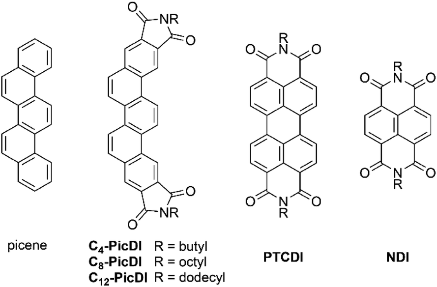 | ||
| Fig. 1 Chemical structures of parent picene, Cn-PicDIs and related aromatic diimides (PTCDI, NDI). | ||
2 Results and discussion
2.1 Synthesis of Cn-PicDIs
The synthetic route to Cn-PicDIs is shown in Scheme 1. The structures of the new compounds were determined by NMR and IR spectra as well as elemental analysis or high-resolution mass spectrometry. The full characterization data and the NMR spectra are deposited in ESI.† Conventionally, phenacene frameworks have been constructed by the Mallory photoreaction.32 Because the photochemical strategy is one of the most convenient and reliable pathways toward phenacene frameworks, we used the photoreaction in the final step.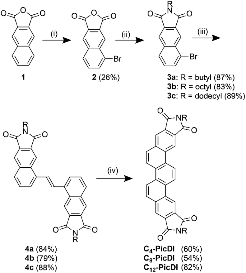 | ||
Scheme 1 Synthetic route to Cn-PicDIs. Reagents and conditions: (i) Br2, NaOH, H2O. (ii) RNH2, AcOH. (iii) (E)-Bu3SnCH![[double bond, length as m-dash]](https://www.rsc.org/images/entities/char_e001.gif) CHSnBu3, Pd(PPh3)4, toluene. (iv) hν (352 nm), I2, air, CH2Cl2. CHSnBu3, Pd(PPh3)4, toluene. (iv) hν (352 nm), I2, air, CH2Cl2. | ||
Bromo-substituted naphthalimides 3a–c were obtained in two steps from commercially available 2,3-naphthalenedicarboxylic anhydride 1. Bromonaphthalimides 3 were efficiently converted to diarylethenes 4 through a Stille coupling reaction with (E)-1,2-bis(tributylstannyl)ethene using Pd(PPh3)4 as a catalyst. Diarylethenes 4a–c were then subjected to Mallory photoreaction, thus, they were irradiated with black-light lamps (352 nm, 6 × 15 W) in the presence of 10 mol% of I2 to afford desired Cn-PicDIs in moderate to good yields. In the photoreaction, the (E)-form of 4 photochemically isomerized to the corresponding (Z)-form which subsequently cyclized to afford Cn-PicDIs.
2.2 Electronic spectra in solution and crystalline states
Fig. 2 shows UV-vis and fluorescence emission spectra of Cn-PicDIs in CHCl3 with those of parent picene as the reference. Parent picene showed absorption bands at λAbsmax 376 nm with small intensity and at 329 nm with moderate intensity. Fluorescence band of picene was observed at λFLmax 378 nm with clear vibrational structure. Cn-PicDIs displayed absorption bands at λAbsmax 408 and 358 nm and fluorescence one at λFLmax 415 nm irrespective of the alkyl chain length at the imide moieties. Therefore, the alkyl chain length little affected the electronic features of Cn-PicDIs in solution. The absorption and fluorescence spectra of Cn-PicDIs red-sifted by 30 nm and 37 nm, respectively, compared to those of parent picene. These results suggest effective conjugation between the picene π system and the two imide moieties. Additionally, the spectral red-shift could be due to contribution from intramolecular charge transfer between the picene core and the imide moieties. As seen from Fig. 3, HOMO of Cn-PicDIs locates on the central picene moiety while LUMO extends over the entire molecule including the imide moieties.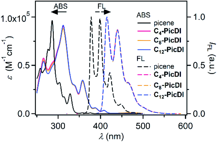 | ||
| Fig. 2 Absorption and fluorescence spectra of Cn-PicDIs and parent picene in CHCl3. | ||
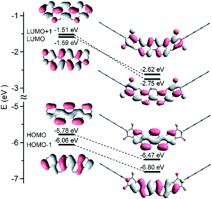 | ||
| Fig. 3 Molecular orbital diagrams for picene (left) and C8-PicDI (right) calculated at the B3LYP/6-31+G(d) level. | ||
Fluorescence emission spectra of Cn-PicDIs were measured in the crystalline state to obtain an insight into their solid state electronic features (Fig. S1 of ESI†). C4-PicDI showed a broad emission band with a maximum at λFLmax 486 nm. C12-PicDI showed an emission profile (λFLmax 473 nm) similar to that of C4-PicDI. In the case of C8-PicDI the emission wavelength region was the same as that of C4- and C12-PicDIs, however, the profile of the emission band was different from that of C4- and C12-PicDIs. These results may indicate that intramolecular interactions were affected by the alkyl chain length of the imide part in the solid state. Unfortunately, single crystals of Cn-PicDIs suitable for X-ray crystallographic analysis were not obtained, we are currently unable to discuss details on the specific intermolecular interactions in solid state.
2.3 Theoretical analysis for the electronic features
Theoretical calculations were performed to investigate electronic features of Cn-PicDIs. The molecular geometries of Cn-PicDIs were optimized by density functional theory (DFT) at the B3LYP/6-31+G(d) level of theory and the optimized atomic coordinates are deposited in Tables S3–S6 of ESI.† Also, the optimized molecular structure of C8-PicDI was shown in Fig. S4 of ESI† as the representative result. The picenediimide core was calculated to be in a flat geometry.Fig. 3 shows molecular orbital (MO) diagrams of C8-PicDI and parent picene. The LUMO energy levels of C8-PicDI (−2.75 eV) was much lower than that of picene (−1.59 eV) suggesting that the charge-transporting state was stabilized by the strongly electron withdrawing imide moieties. The imide moieties effectively interact with the electronic core of picene in C8-PicDI to modify the molecular orbital levels. As a result, the LUMO and LUMO+1 levels are inverted between parent picene and C8-PicDI. C4-PicDI and C12-PicDI showed the same electronic features as C8-PicDI. The LUMO of C8-PicDI has less nodal planes along the long axis of the molecule compared to the case of parent picene. It is, thus, expected that such an electronic nature facilitates efficient overlapping of the molecular orbitals resulting in strong interactions between Cn-PicDI molecules in the charge-transporting state in solid state.13
2.4 Structures and electronic properties in thin films
Fig. 4(a) shows X-ray diffraction (XRD) patterns of thin films of Cn-PicDIs exhibiting only 00l Bragg reflections; the process of fabrication of the thin films is the same as that for the thin films for FET devices (see ESI†). The 1/|c*| values were determined to be 22.94(7) Å, 31.0(1) Å and 37.1(6) Å, respectively, for n = 4, 8 and 12; c* refers to the reciprocal lattice of lattice constant, c. The increase in 1/|c*| against n is reasonable because the long-axis length of Cn-PicDIs extends with n, i.e., the long axis of Cn-PicDI molecules stands with almost normal to the substrate. Actually, as seen from Fig. 4(b), the long axis of Cn-PicDIs (n = 4, 8 and 12) are inclined by 30°, 29° and 32°, respectively, with respect to c* axis. This inclined angle (θ) is almost the same as that, ca. 30°, of (C14H29)2-picene.19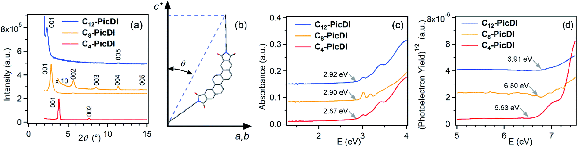 | ||
| Fig. 4 (a) XRD patterns of thin films of Cn-PicDIs formed on an SiO2 substrate. (b) Orientation of the long axis of the Cn-PicDI molecule with respect to c* axis (normal to ab plane) in the thin film formed on an SiO2 substrate. (c) Electronic absorption spectra of thin films of Cn-PicDIs formed on quartz glass. (d) PYS spectra of thin films of Cn-PicDIs formed on SiO2/Si substrate. | ||
As seen from Fig. 4(c), the electronic absorption spectra of thin films of Cn-PicDIs show that the onset energy changes slightly from 2.87 eV to 2.92 eV with an increase in n, indicating that the HOMO–LUMO gap does not vary significantly with extended alkyl chains. On the other hand, the photoelectron yield spectroscopy (PYS) (Fig. 4(d)) shows that the onset energy increases gradually from 6.63 eV to 6.91 eV with an increase in n. This implies that the HOMO level lowers with n.
Fig. 5 shows the energy levels of HOMO and LUMO determined experimentally for Cn-PicDIs in comparison to parent picene and N,N′-dioctyl-3,4:9,10-perylenedicarboximide (PTCDI-C8, see Fig. 1 for structure, R = octyl) as the reference materials. The LUMO levels are located in an energy range of −3.76 eV to −3.99 eV, indicating that the LUMO level lies in the lower energy range than the LUMO levels (−2.2 eV to −2.9 eV) of parent phenacene molecules33 which have provided good p-channel FET operation. The energy (−3.76 eV to −3.99 eV) for the LUMO levels of Cn-PicDIs suggests a potential n-channel FET operation.
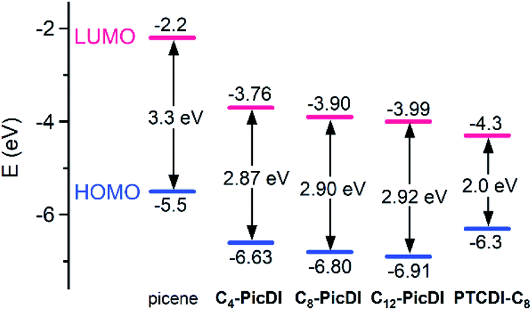 | ||
| Fig. 5 Energy diagrams for HOMO and LUMO of picene, Cn-PicDIs, and PTCDI-C8 experimentally determined by PYS and electronic absorption spectra in thin films. The data for picene and PTCDI-C8 are taken from ref. 16 and 34, respectively. | ||
It is important to reveal structure-mobility relationship to design a novel n-channel material. For CnPicDIs, single crystals appropriate for X-ray crystallographic analysis were not obtained in this study. Detailed structural analysis for Cn-PicDIs in crystalline and thin films are underway.
2.5 n-Channel FET characteristics
Fig. 6(a) shows a device structure of Cn-PicDI thin-film FET with a ZrO2 gate dielectric; the commercially available ZrO2 thin film prepared by RF sputtering was used in this study. The device structure corresponds to a typical top-contact bottom-gate type. Details of device fabrication procedure are described in experimental section of ESI.† A 3 nm thick 2,3,5,6-tetrafluorotetracyanoquinodimethane (F4TCNQ) layer was inserted to reduce contact resistance between the active layer and source (S)/drain (D) electrodes (Fig. 6(a)). Here, it should be stressed that F4TCNQ is not doped to the channel region but underneath the electrodes. Namely, only contact resistance is decreased by the F4TCNQ doping. The transfer and output characteristics of C8-PicDI thin-film FET measured under an argon atmosphere are shown in Fig. 6(b) and (c), respectively, which show typical n-channel normally-off FET characteristics. Thus, as expected from the energy diagram shown in Fig. 5, a clear n-channel operation was obtained.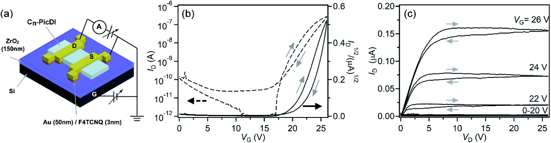 | ||
| Fig. 6 (a) Device structure of Cn-PicDI FETs. (b) Transfer and (c) output curves of C8-PicDI thin-film FETs with ZrO2 gate dielectric. This FET refers to device #5 in Table 1. | ||
The FET parameters for seven C8-PicDI thin-film FET devices are listed in Table 1. The values of averaged μ (〈μ〉) and Vth (〈Vth〉) are 1.0(6) × 10−1 cm2 V−1 s−1 and 20(2) V, respectively. All measurements of FET properties were done in Ar atmosphere (see ESI†). The maximum field-effect mobility (μ) was determined to be 2.0 × 10⁻¹ cm2 V−1 s−1 from the transfer curve (Fig. 6(b)) in the saturation regime with normal formula.35 The above μ value is relatively high in n-channel organic thin-film FETs, i.e., the value is almost the same as that in PTCDI-C8 thin-film FET which is normally employed for n-channel FET.24–26 Also the relatively low voltage operation (Vth = 20.4 V) is achieved in C8-PicDI thin-film FET because of the usage of high-k gate dielectric (ZrO2), but the Vth value is a little higher in comparison with that (Vth ∼ 2.9 V) of PTCDI-C8 thin film FET using ZrO2 gate dielectric (evaluated in this study, data not shown). This is due to higher LUMO level of Cn-PicDIs than that of PTCDI-C8 as seen from Fig. 4. Herein, we comment a little large hysteresis observed in transfer and output curves (Fig. 6(b) and (c)). The hysteresis may be due to the bias stress effect, which is observed in non-hydrophobic surface of gate dielectric. Therefore, a parylene-coating of ZrO2 employed in this study may not provide a sufficient hydrophobic surface. This must be further ameliorated.
| Sample | μ (cm2 V−1 s−1) | VTH (V) | on/off | S (V per decade) |
|---|---|---|---|---|
| a The parameters were determined from the forward transfer curves. | ||||
| #1 | 0.64 × 10⁻¹ | 18.8 | 2.0 × 10⁴ | 1.87 |
| #2 | 1.4 × 10⁻¹ | 17.2 | 6.4 × 10⁴ | 1.08 |
| #3 | 0.95 × 10⁻¹ | 17.5 | 3.7 × 10⁴ | 1.24 |
| #4 | 0.22 × 10⁻¹ | 20.0 | 1.0 × 10⁴ | 1.78 |
| #5 | 2.0 × 10⁻¹ | 20.4 | 2.6 × 10⁴ | 0.890 |
| #6 | 0.98 × 10⁻¹ | 21.5 | 1.5 × 10⁴ | 1.05 |
| #7 | 1.0 × 10⁻¹ | 21.5 | 1.7 × 10⁴ | 1.00 |
| Average | 1.0(6) × 10−1 | 20(2) | 3(2) × 104 | 1.3(4) |
The FET characteristics of C4-PicDI and C12-PicDI thin-film FETs with ZrO2 gate dielectric also showed n-channel normally-off FET properties (see Fig. S2 and S3 of ESI† for the transfer and output curves). Tables S1 and S2 of ESI† list the FET parameters of four C4-PicDI thin-film FETs and eight C12-PicDI thin-film FETs, respectively. The highest μ values for C4-PicDI and C12-PicDI thin-film FETs were 2.7 × 10⁻⁴ cm2 V−1 s−1 and 1.9 × 10⁻² cm2 V−1 s−1, respectively. Thus, the μ value for C4-PicDI thin-film FET was two-three orders of magnitude lower than that for C8-PicDI and C12-PicDI. At the present stage, C8-PicDI provides the highest μ value among the Cn-PicDIs investigated. The reason is still unclear, but the higher energy level of LUMO (−3.76 eV) might provide the poorer FET properties of C4-PicDI. In addition, the difference in μ between C8-PicDI and C12-PicDI may not be due to the energy levels of LUMO (−3.90 eV for C8-PicDI and −3.99 eV for C12-PicDI) but the crystallinity of thin films i.e., poorer crystallinity in C12-PicDI thin film as seen from the XRD patterns (Fig. 4(a)). As a consequence, the best material for n-channel FET operation is C8-PicDI among the Cn-PicDI molecules. Such suitable alkyl chains for active layers of FET devices are reported for various organic semiconductor compounds.10,36 Admittedly, C8-PicDI would be a promising material for n-channel FET operation owing to the high μ value as high as 2.0 × 10⁻¹ cm2 V−1 s−1. In addition, the FET properties were not recorded in ambient atmosphere, but it would be very important because n-channel operation drastically degrades under air. This would be a future significant work.
Finally, we briefly comment FET properties of Cn-PicDI thin-film FETs with an SiO2 gate dielectric. n-Channel properties were found for the C4-PicDI and C8-PicDI thin-film FETs by applying higher voltage than 90 V, but the observed Id value was lower than 10−9 A above 120 V; the Vth values were 110 V for C4-PicDI and 98 V for C8-PicDI. The results indicate that high-k gate dielectric is required for stable n-channel operation in Cn-PicDI thin-film FETs. From these points, the Vth value of 20(2) V in C8-PicDI thin-film FET with ZrO2 gate dielectric may be prominent.
3 Conclusions
Picene derivatives bearing imide moieties at the both edges of the molecule (Cn-PicDIs) were successfully synthesized by using the Mallory photoreaction as the key step. Cn-PicDIs are, to the best of our knowledge, the first phenacene derivatives possessing imide moieties in the long-axis direction of the framework. It was revealed that Cn-PicDIs served as the active layer of n-channel FET devices with high electron mobility. The highest μ value recorded for C8-PicDI (2.0 × 10⁻¹ cm2 V−1 s−1) was comparable to μ values of PTCDIs which were benchmark molecules of n-channel FET materials. Moreover, we point out that the usage of Ag metal for source/drain electrodes may lead to the higher value of μ owing to the reduction of carrier injection barrier height. This would be a future task. The present results would contribute to molecular design of new n-channel organic semiconductors which are highly desired in the current organic electronics.Conflicts of interest
There are no conflicts to declare.Acknowledgements
The present study was partly supported by Grants-in-Aid for Scientific Research, KAKENHI, from MEXT (26105004, 17K05976, 17K05500, 18K04940, 18K18736, 19H02676 and 20K05648) and by the Cooperative Research Program of the ‘Network Joint Research Center for Materials and Devices’ from MEXT, Japan. This work was the result of using research equipment shared in MEXT Project for promoting public utilization of advanced research infrastructure (program for supporting introduction of the new sharing system) Grant Number JPMXS0422300120.Notes and references
- S. R. Forrest, Nature, 2004, 428, 911–918 CrossRef CAS PubMed.
- G. Schweicher, G. Garbay, R. Jouclas, F. Vibert, F. Devaux and Y. H. Geerts, Adv. Mater., 2020, 1905909 CrossRef CAS PubMed.
- Y. Xu, C. Liu, D. Khim and Y.-Y. Noh, Phys. Chem. Chem. Phys., 2015, 17, 26553–26574 RSC.
- J. Yang, B. Xiao, A. Tang, J. Li, X. Wang and E. Zhou, Adv. Mater., 2019, 31, 1804699 CrossRef CAS PubMed.
- C. Zhao, J. Wang, J. Jiao, L. Huang and J. Tang, J. Mater. Chem. C, 2020, 8, 28–43 RSC.
- C. Lee, S. Lee, G.-U. Kim, W. Lee and B. J. Kim, Chem. Rev., 2019, 119, 8028–8086 CrossRef CAS PubMed.
- C. Wang, H. Dong, L. Jiang and W. Hu, Chem. Soc. Rev., 2018, 47, 422–500 RSC.
- J. Mei, Y. Diao, A. L. Appleton, L. Fang and Z. Bao, J. Am. Chem. Soc., 2013, 135, 6724–6746 CrossRef CAS PubMed.
- Y. Yuan, G. Giri, A. L. Ayzner, A. P. Zoombelt, S. C. B. Mannsfeld, J. Chen, D. Nordlund, M. F. Toney, J. Huang and Z. Bao, Nat. Commun., 2014, 5, 3005 CrossRef PubMed.
- K. Takimiya, I. Osaka, T. Mori and M. Nakano, Acc. Chem. Res., 2014, 47, 1493–1502 CrossRef CAS PubMed.
- H. Iino, T. Usui and J. Hanna, Nat. Commun., 2015, 6, 6828 CrossRef CAS PubMed.
- K. Nakayama, Y. Hirose, J. Soeda, M. Yoshizumi, T. Uemura, M. Uno, W. Li, M. J. Kang, M. Yamagishi, Y. Okada, E. Miyazaki, Y. Nakazawa, A. Nakao, K. Takimiya and J. Takeya, Adv. Mater., 2011, 23, 1626–1629 CrossRef CAS PubMed.
- C. Mitsui, T. Okamoto, M. Yamagishi, J. Tsurumi, K. Yoshimoto, K. Nakahara, J. Soeda, Y. Hirose, H. Sato, A. Yamano, T. Uemura and J. Takeya, Adv. Mater., 2014, 26, 4546–4551 CrossRef CAS PubMed.
- A. Yamamoto, Y. Murata, C. Mitsui, H. Ishii, M. Yamagishi, M. Yano, H. Sato, A. Yamano, J. Takeya and T. Okamoto, Adv. Sci., 2018, 5, 1700317 CrossRef PubMed.
- T. Okamoto, C. P. Yu, C. Mitsui, M. Yamagishi, H. Ishii and J. Takeya, J. Am. Chem. Soc., 2020, 142, 9083–9096 CrossRef CAS PubMed.
- H. Okamoto, N. Kawasaki, Y. Kaji, Y. Kubozono, A. Fujiwara and M. Yamaj, J. Am. Chem. Soc., 2008, 130, 10470–10471 CrossRef CAS PubMed.
- Y. Kubozono, X. He, S. Hamao, K. Teranishi, H. Goto, R. Eguchi, T. Kambe, S. Gohda and Y. Nishihara, Eur. J. Inorg. Chem., 2014, 3806–3819 CrossRef CAS.
- Y. Shimo, T. Mikami, S. Hamao, H. Goto, H. Okamoto, R. Eguchi, S. Gohda, Y. Hayashi and Y. Kubozono, Sci. Rep., 2016, 6, 21008 CrossRef CAS PubMed.
- H. Okamoto, S. Hamao, H. Goto, Y. Sakai, M. Izumi, S. Gohda, Y. Kubozono and R. Eguchi, Sci. Rep., 2014, 4, 5048 CrossRef CAS PubMed.
- E. Pompei, C. Turchetti, S. Hamao, A. Miura, H. Goto, H. Okamoto, A. Fujiwara, R. Eguchi and Y. Kubozono, J. Mater. Chem. C, 2019, 7, 6022–6033 RSC.
- Y. Shimo, T. Mikami, H. T. Murakami, S. Hamao, H. Goto, H. Okamoto, S. Gohda, K. Sato, A. Cassinese, Y. Hayashi and Y. Kubozono, J. Mater. Chem. C, 2015, 3, 7370–7378 RSC.
- Y. Sakamoto, T. Suzuki, M. Kobayashi, Y. Gao, Y. Fukai, Y. Inoue, F. Sato and S. Tokito, J. Am. Chem. Soc., 2004, 126, 8138–8140 CrossRef CAS PubMed.
- M. A. Kobaisi, S. V. Bhosale, K. Latham, A. M. Raynor and S. V. Bhosale, Chem. Rev., 2016, 116, 11685–11796 CrossRef CAS PubMed.
- X. Zhan, A. Facchetti, S. Barlow, T. J. Marks, M. A. Ratner, M. R. Wasielewski and S. R. Marder, Adv. Mater., 2011, 23, 268–284 CrossRef CAS PubMed.
- M. Gsänger, D. Bialas, L. Huang, M. Stolte and F. Würthner, Adv. Mater., 2016, 28, 3615–3645 CrossRef PubMed.
- F. Würthner and M. Stolte, Chem. Commun., 2011, 47, 5109–5115 RSC.
- M. Chu, J.-X. Fan, S. Yang, D. Liu, C. F. Ng, H. Dong, A.-M. Ren and Q. Miao, Adv. Mater., 2018, 30, 1803467 CrossRef PubMed.
- J.-H. Dou, Y.-Q. Zheng, Z.-F. Yao, Z.-A. Yu, T. Lei, X. Shen, X.-Y. Luo, J. Sun, S.-D. Zhang, Y.-F. Ding, G. Han, Y. Yi, J.-Y. Wang and J. Pei, J. Am. Chem. Soc., 2015, 137, 15947–15956 CrossRef CAS PubMed.
- R. Wang, K. Shi, K. Cai, Y. Guo, X. Yang, J.-Y. Wang, J. Pei and D. Zhao, New J. Chem., 2016, 40, 113–121 RSC.
- T. S. Moreira, M. Ferreira, A. Dall'armellina, R. Cristiano, H. Gallardo, E. A. Hillard, H. Bock and F. Durola, Eur. J. Org. Chem., 2017, 4548–4551 CrossRef CAS.
- G. Naulet, S. Huet-Exiga, H. Bock and F. Durola, Org. Chem. Front., 2019, 6, 994 RSC.
- F. B. Mallory and C. W. Mallory, Org. React., 1984, 30, 1–456 CAS.
- H. Okamoto, S. Hamao, R. Eguchi, H. Goto, Y. Takabayashi, Y.-H. Yen, L. U. Liang, C.-W. Chou, G. Hoffmann, S. Gohda, H. Sugino, Y. Liao, H. Ishii and Y. Kubozono, Sci. Rep., 2019, 9, 4009 CrossRef PubMed.
- N. Hiroshiba, R. Hayakawa, T. Chikyow, Y. Yamashita, H. Yoshikawa, K. Kobayashi, K. Morimoto, K. Matsuishi and Y. Wakayama, Phys. Chem. Chem. Phys., 2011, 13, 6280–6285 RSC.
- S. M. Sze, Semiconductor Devices: Physics and Technology, 2nd ed., John Willey & Sons, Inc., UK, 2001 Search PubMed.
- H. Inokuchi, G. Saito, P. Wu, K. Seki, T. B. Tang, T. Mori, K. Imaeda, T. Enoki, Y. Higuchi, K. Inaka and N. Yasuoka, Chem. Lett., 1986, 15, 1263–1266 CrossRef.
Footnote |
| † Electronic supplementary information (ESI) available: Experimental details, FET parameters of Cn-PicDIs, NMR spectra of new compounds, theoretical calculation results. See DOI: 10.1039/d0ra06629j |
| This journal is © The Royal Society of Chemistry 2020 |