
 Open Access Article
 This Open Access Article is licensed under a Creative Commons Attribution-Non Commercial 3.0 Unported Licence
Shape-dependent close-edge 2D-MoS2 nanobelts †
Xiaofeng Wang‡
ab,
Haiguang Yang‡ab,
Huimin Feng‡ ab,
Lei Wangc,
Shengyao Chenad,
Zhican Zhouad,
Shu Wangab and
Qian Liu*abd
ab,
Lei Wangc,
Shengyao Chenad,
Zhican Zhouad,
Shu Wangab and
Qian Liu*abd
aChinese Academy of Sciences (CAS) Key Laboratory of Nanosystem and Hierarchical Fabrication, CAS Center for Excellence in Nanoscience, National Center for Nanoscience and Technology, Beijing 100190, P. R. China. E-mail: liuq@nanoctr.cn
bUniversity of Chinese Academy of Sciences, Beijing 100049, P. R. China
cCollege of Mathematics and Physics, Shandong Advanced Optoelectronic Materials and Technologies Engineering Laboratory, Qing Dao University of Science and Technology, Qingdao 266061, China
dThe MOE Key Laboratory of Weak-Light Nonlinear Photonics and TEDA Applied Physics Institute and School of Physics, Nankai University, Tianjin 300457, China
First published on 10th September 2020
Abstract
Atomic-thin MoS2 materials have attracted increasing attention due to their potentials in numerous fields. However, in 2D-MoS2 sheets, the edge region usually has unique features differing from the interior region, which has potential application in enhancing catalysts and shape-dependent 2D-nanodevices. However, fabricating it cost-effectively is still very difficult. Here, we present one universal method to obtain various shape-dependent closed-edge 2D-MoS2 nanobelts only using one simple step, and width of the MoS2 nanobelts (minimum of 270 nm) were adjustable. Our strategy opens a new fabrication route for closed-edge 2D-MoS2 nanobelts, and in principle, this method is also suitable for other CVD-grown 2D materials.
Introduction
Two dimensional (2D) MoS2, as a star material of 2D transition metal dichalcogenide (TMD) family, has numerous potential applications in the fields of electronics,1,2 optoelectronics,3 flexible and wearable devices,4 and catalysis5 due to its unique physical and chemical properties. With the rapid development of research on MoS2, patterning MoS2 has been paid increasing attention for various shape-dependent nanodevices. Several patterned MoS2 materials have been fabricated, such as growth and etch,6 shadow mask,7 laser cutting,8 and recyclable masked growth.9 Recently, some studies found that the edge region of CVD-grown MoS2 sheets has different properties in photonics and catalysis compared to the interior region.10 This implies that the closed-edge nanobelts of MoS2 have potential applications in some shape-dependent 2D-nanodevices, particularly in enhancing catalysis, due to the edge region having a large amount of dangling bonds which are easy to be chemical modification. Therefore, it is necessary to obtain MoS2 closed-edge nanobelts. Although such edge nanobelts can be tailored by some technologies such as, FIB (focused ion beam) technology and electron beam lithography (EBL), they need expensive equipment, thus stimulating to develop more cost-effective fabrication method.In this study, we presented a very simple mechanical peeling method and successfully obtained various closed and shape-dependent MoS2 edge nanobelts. By controlling the adhesion layer covering the MoS2 sheet, we can obtain different width MoS2 closed-edge belts, having a minimum width of 270 nm. The spectra of the 2D-MoS2 show obvious differences between the edge region and the interior region. Our method opens a feasible route for fabricating numerous shape-dependent closed-edge 2D-MoS2 nanobelts, and in principle, this method is also suitable for other 2D-TMDs.
Experimental
Growth of 2D-MoS2
MoS2 was grown on a 300 nm-SiO2/Si substrate using a molten-salt-assisted CVD method. Sulfur (S) powder (10 mg), MoO3 (0.79 mg) and NaCl (0.16 mg) was used as the S source, Mo source and catalyst, respectively. The substrate faced down to both the Mo source and catalyst in a quartz boat in a tube furnace, and the S source was placed in another boat located in the upstream position of the furnace. The distance between the two boats is 18 cm. The vacuum degree of the furnace was first set to 0.1 torr, and then Ar gas (gas flow of 85 sccm) was injected into the furnace. When the pressure of the furnace was close to ambient pressure, heating was set to 800 °C and maintained for 10 min. Finally, MoS2 sheets were taken out after the furnace was cooled naturally to room temperature.Separation of MoS2 edge nanobelts
The bottom adhesion solution was prepared by putting PVP (0.75 g, Macklin, average MW 58000) into a mixed solution [1.5 ml-NVP (Aladdin, 99%), 1.5 ml-water and 7.5 ml ethanol solution], and then the mixture was spin-coated on the surface of MoS2 at a setting speed (typical for 4000 rpm). Furthermore, the sample was baked at 90 °C for 15 s to remove residual solvent. After that, a 10 wt% PVA (Aladdin, 97.5–99% hydrolysed, high molecular weight) aqueous solution was spin-coated on the sample using 4000 rpm and baked at 90 °C for 1 min. By slowly peeling off the adhesion film on the MoS2 using a tweezer, the interior region of the MoS2 sheet was peeled off and only the closed-edge nanobelt of the MoS2 sheet was left on the substrate.MoS2 transferring onto TEM lacey carbon films
MoS2 closed-edge nanobelts were spin-coated with polymethyl methacrylate (PMMA) at 1000 rpm and baked at 100 °C for 5 min. Then, the closed-edge nanobelts were put into an ultrasonic machine (YKTD-240W) with water for 5 min at 240 W. After the PMMA/MoS2 film floated on the water surface, it was transferred onto a TEM lacey carbon film and baked at 90 °C for a while to remove water. Subsequently, PMMA was removed by acetone, and the sample on the lacey carbon film was prepared for TEM test.Characterization and measurement of MoS2 edge nanobelts
The morphologies were measured using a laser scanning confocal microscope (Olympus, LEXT-OLS4000) and scanning electron microscope (SEM, Hitachi-SU8220). The height was recorded using an atomic force microscope (AFM, Bruker Multimode HR8). Raman spectra and photoluminescence spectra were recorded with a laser excitation wavelength of 532 nm at room temperature (Renishaw inVia plus). The transmission electron microscope (TEM) observations were performed at 200 kV (Tecnai G2 F20 U-TWIN).Results and discussion
Closed and shape-dependent edge nanobelts
In our experiments, we synthesized high-quality MoS2 via a molten-salt-assisted CVD method.11 Fig. 1(a) is a schematic diagram of the experimental process. Triangle single-layer monocrystal MoS2 sheets were grown on the surface of the 300 nm-SiO2/Si substrate, and their optical microscope (OM) image is displayed in Fig. 1(b). The adhesion layer composed of two different material films was in turn spin-coated on the as-grown MoS2. It should be noted that the adhesion layer has a great influence on the obtained edge nanobelts. Here, the bottom film is a mixture of N-vinylpyrrolidone (NVP), polyvinylpyrrolidone (PVP) and water (H2O) in ethanol, and the top film is 10% poly (vinyl alcohol) (PVA) solution (see Experimental for details). After baking, the adhesion layer was slowly peeled off using tweezers, while the interior region in each triangle MoS2 sheet was exfoliated along with the adhesion layer but the triangle outer closed nanobelts were left on the surface of SiO2. Fig. 1(c and d) are the OM image and SEM image of the single-layer-MoS2 closed-edge nanobelts, respectively. The enlarged SEM image in Fig. 1(d) shows that the narrowest closed-edge MoS2 nanoribbons is 270 nm. The height of MoS2 edge nanobelts is approximately 1.1 nm according to the AFM measurement, as shown in Fig. 1(e), which is slightly higher than that of the as-grown single layer MoS2 (see ESI Fig. 1†). This may be caused by tension stress generated at the edge belt, leading to a slight increase in the height due to the peeling action.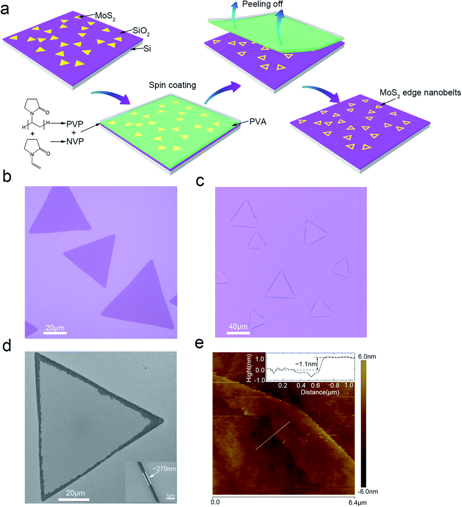 | ||
| Fig. 1 Edge nanobelt of MoS2. (a) Schematic for the separation process. (b) OM of as-grown MoS2. (c) OM of a MoS2 edge nanobelt. (d) SEM image of a MoS2 edge nanobelt (about 270 nm in inset). (e) AFM morphology of a MoS2 edge nanobelt and height (inset). | ||
Except for triangle MoS2 edge nanobelts, we can also obtain various shape-dependent MoS2 edge nanobelts by the same peeling method, such as differently shaped single-layer edge nanobelts (Fig. 2(a–j)) and bilayer-MoS2 edge nanobelts (Fig. 2(k and l)). Herein, the shape of MoS2 sheets is mainly determined by the ratio of Mo and S during the CVD growth process.12 Irrespective of the shape of MoS2 grown by the CVD process, the edge nanobelts can always be obtained via exfoliation, indicating the universality of the peeling method.
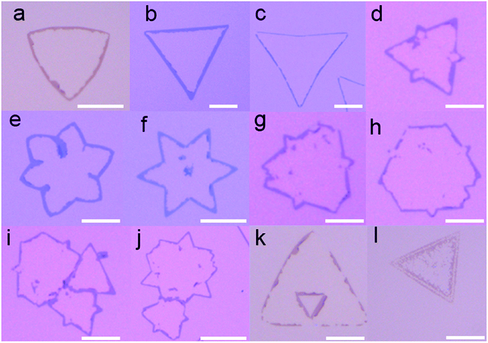 | ||
| Fig. 2 Various shape nanobelts of monocrystal and polycrystal MoS2. (a–j). Different shape nanobelts of single layer MoS2. (k and l). Nanobelts of double layer MoS2. All Scale bars are 20 μm. (The different color of background are caused by objective lens with different magnification). | ||
Crystalline feature of MoS2 edge nanobelts
Complete crystallinity is important in numerous potential applications. The mechanical separation process may affect the MoS2 edge nanobelt crystal structure because the as-grown MoS2 has very high Young's modulus (∼270 GPa13,14). To clarify the crystal structure of MoS2 edge nanobelts, wet transfer was employed (see Experimental for details) to transfer the MoS2 edge nanobelts onto the lacey carbon films. Fig. 3(a) demonstrates the complete MoS2 edge nanobelt on the carbon film. Low magnification TEM shows partial of the nanobelt in Fig. 3(b). High resolution TEM in Fig. 3(c) shows that the (100) crystal plane with a spacing of 0.27 nm agrees with the literature.15 A selected area electron diffraction (SAED) image shown in Fig. 3(d) further confirms the single crystal feature of the edge nanobelts. The monocrystal feature can also be identified in the Raman spectra on the edge nanobelt on the lacey carbon film (see ESI Fig. 2†).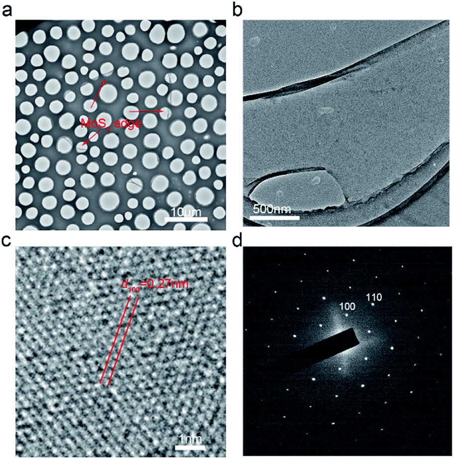 | ||
| Fig. 3 Crystal structure characterization for edge frame of MoS2. (a) Complete edge frame of MoS2 indicated by red arrows. (b and c) Low-magnification TEM and HRTEM for the edge region MoS2. (d) Corresponding electron area selective diffraction. | ||
However, during the peeling process, there is residual stress produced in the edge regions. Stress will induce different features between the edge regions and the interior regions, as shown PL spectra and Raman spectra (see ESI Fig. 3†). This will provide many new application opportunities for the 2D-MoS2 material.
Width adjustment of edge belts and mechanism of separation
In order to adjust the width of the edge nanobelts and clarify the separation mechanism of the closed-edge nanobelts. We prepared adhesion layers with different experimental conditions. Here, the PVA top film mainly provided the mechanical strength, while the bottom film composed of NVP, PVP, H2O and C2H5OH was contacted directly with the as-prepared MoS2 sheet and played an essential role in the separation process.The separation process is determined by two factors: (1) the conformal contact of the adhesion solution with the MoS2 sheet and (2) the sufficient adhesion force from the adhesion layer. NVP enables the conformal coating of the adhesion solution on the surface of MoS2,16 which can be realized by controlling the centrifugal force in the spin-coating process. Fig. 4(a–c) show the impact of different centrifugal forces on adhesion. A mixed solution of 1.5 ml-NVP, 0.4 g-PVP, 1.5 ml-water and 7.5 ml-ethanol was spin-coated on the as-grown MoS2 sheet at 3000 rpm, 4000 rpm and 5000 rpm, respectively. The higher the rotation speed, the thinner bottom film is (see ESI Fig. 4†). In addition, the edge nanobelt width has a gradual decrease with an increase in the centrifugal force, as shown in Fig. 4(d).
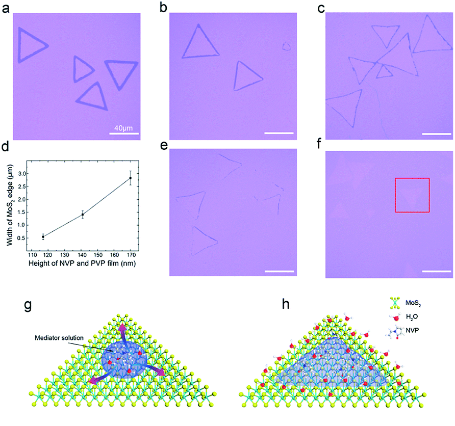 | ||
| Fig. 4 Control of the edge belts width. (a–c) The adhesion film spin-coated at 3000 rpm, 4000 rpm. 5000 rpm, respectively. The adhesion solution component was NVP (1.5 ml), PVP (0.4 g), water (1.5 ml) and ethanol (7.5 ml). (d) Edge belts width changing with the bottom-layer adhesion thickness. (e and f) The adhesion solution component was PVP (0.5 g), and PVP (0.75 g) in NVP (1.5 ml), water (1.5 ml) and ethanol (7.5 ml), respectively, and spin-coated at 4000 rpm. (g and h) Schematic of the separation mechanism. (g) Droplet before spin-coating. (h) Droplet after spin-coating. All Scale bars are 40 μm. | ||
PVP is the polymer of NVP, which mainly plays a role of strong adhesive force.17 With the increase in the PVP concentration in the solution from 0.4 g to 0.5 g and to 0.75 g, the adsorption force of the adhesion layer on MoS2 gradually increases, as shown in Fig. 4(b, e and f), thus making the edge belt width gradually decrease. When the PVP content reached 0.75 g, the as-grown MoS2 sheet could be entirely peeled off using the adhesion layer, as shown in red box in Fig. 4(f).
Different wettability between the edge and interior region in an MoS2 sheet has a decisive effect on the separation of the edge belt. The contact angle of water on the surface of the MoS2 sheet is close to 90°, displaying nearly a hydrophobic feature. Compared with the interior region, the edge belt easily adsorbs water molecules because of the higher activity of the dangling bonds existing in the edge region. It should be noted that at a low rotation speed, NVP in the adhesion solution can mainly gather in the centre of the MoS2 sheet, resulting in the edge region to uncover by the adhesion after rapid baking. With an increase in the centrifugal force, the adhesion solution is gradually spread to the edge region of the MoS2 sheet and drives water molecules in whole MoS2, aggregating to the edge region and causing the edge region to remain in a peeling action. Therefore, the edge nanobelt is narrower in a larger centrifugal force for a certain PVP solution, a schematic is shown in Fig. 4(g and h). The minimum width obtained in our experiment is about 270 nm. In addition, the edge belts of bilayer MoS2 can be also separated by utilizing wettability difference between the two layers,18 as shown in Fig. 2(k and l).
Actually, various shape-dependent monocrystal MoS2 edge belts with different shapes and number of layers, even polycrystalline MoS2 belts shown in Fig. 2(i and j) can all be obtained by our technique, indicating that the method is universal to 2D MoS2 materials. Owing to the same separation principle, our method might also be suitable for other TMD materials grown via CVD, such as WS2 (see ESI Fig. 5†). More interestingly, such nanobelts are similar to TMDs ribbons, which are commonly fabricated by CVD synthesis,19,20 water etching,21 EBL and FIB technologies22 etc. Compared with these methods, our method is simpler in spite of some limit in shape. Isolated edge nanobelts are significant for study on the difference between the edge region and interior region, including electrical, magnetic, and catalytic properties. Moreover, we look forward to emerging practical applications of various 2D materials edge belts.
Conclusions
By mechanical peeling based on different wettabilities between the edge region and interior region, a simple and universal method to separate edge nanobelts from MoS2 sheet grown via molten-salt-assisted CVD has been presented. Different number of layers and various shape-dependent width-tuning MoS2 closed-edge nanobelts (the narrowest 270 nm) have been demonstrated in the experiment, and the separation mechanism of the edge belts has also been cleared. The simple fabrication method for shape-dependent closed-edge nanobelts provides numerous new opportunities for studying the electrical and magnetic properties and catalytic performance in the edge region of various 2D-TMDs materials and various shape-dependent 2D-material nanodevices.Conflicts of interest
There are no conflicts to declare.Acknowledgements
This work was supported by the National Key Research and Development Program of China (2016YFA0200403), the National Natural Science Foundation of China (51971070, 10974037), the CAS Strategy Pilot Program (XDA 09020300), and Eu-FP7 Project (No. 247644).Notes and references
- T. Liu, S. Liu, K. H. Tu, H. Schmidt, L. Chu, D. Xiang, J. Martin, G. Eda, C. A. Ross and S. Garaj, Nat. Nanotechnol., 2019, 14, 223–226 CrossRef.
- H. M. Li, D. Lee, D. S. Qu, X. C. Liu, J. J. Ryu, A. Seabaugh and W. J. Yoo, Nat. Commun., 2015, 6, 6564 CrossRef.
- M. S. Choi, D. Qu, D. Lee, X. Liu, K. Watanabe, T. Taniguchi and W. J. Yoo, ACS Nano, 2014, 8, 9332–9340 CrossRef.
- T. Dong, J. Simões and Z. Yang, Adv. Mater. Interfaces, 2020, 7, 1901657 CrossRef.
- P. Cheng, Q. Zhou, X. Hu, S. Su, X. Wang, M. Jin, L. Shui, X. Gao, Y. Guan, R. Nozel, G. Zhou, Z. Zhang and J. Liu, ACS Appl. Mater. Interfaces, 2018, 10, 23444–23450 CrossRef.
- H. Zhou, et al., Nano Res., 2013, 6, 703–711 CrossRef.
- W. Park, et al., ACS Nano, 2014, 8, 4961–4968 CrossRef.
- L. Cao, et al., Small, 2013, 9, 2905–2910 CrossRef CAS.
- Y. Guo, et al., Proc. Natl. Acad. Sci. U.S.A, 2019, 116, 3437–3442 CrossRef CAS.
- W. Bao, N. J. Borys, C. Ko, J. Suh, W. Fan, A. Thron, Y. J. Zhang, A. Buyanin, J. Zhang, S. Cabrini, P. D. Ashby, A. Weber-Bargioni, S. Tongay, S. Aloni, D. F. Ogletree, J. Q. Wu, M. B. Salmeron and P. J. Schuck, Nat. Commun., 2015, 6, 7993 CrossRef CAS.
- J. D. Zhou, J. H. Lin, X. W. Huang, Y. Zhou, Y. Chen, J. Xia, H. Wang, Y. Xie, H. M. Yu, J. C. Lei, D. Wu, F. C. Liu, Q. D. Fu, Q. S. Zeng, C. H. Hsu, C. L. Yang, L. Lu, T. Yu, Z. X. Shen, H. Lin, B. I. Yakobson, Q. Liu, K. Suenaga, G. T. Liu and Z. Liu, Nature, 2018, 556, 355–359 CrossRef CAS.
- S. S. Wang, Y. M. Rong, Y. Fan, M. Pacios, H. Bhaskaran, K. He and J. H. Warner, Chem. Mater., 2014, 26, 6371–6379 CrossRef CAS.
- K. Liu, Q. Yan, M. Chen, W. Fan, Y. Sun, J. Suh, D. Fu, S. Lee, J. Zhou, S. Tongay, J. Ji, J. B. Neaton and J. Wu, Nano Lett., 2014, 14, 5097–5103 CrossRef CAS.
- N. Iguiniz, R. Frisenda, R. Bratschitsch and A. Castellanos-Gomez, Adv. Mater., 2019, 31, e1807150 CrossRef.
- D. Ma, J. Shi, Q. Ji, K. Chen, J. Yin, Y. Lin, Y. Zhang, M. Liu, Q. Feng, X. Song, X. Guo, J. Zhang, Y. Zhang and Z. Liu, Nano Res., 2015, 8, 3662–3672 CrossRef CAS.
- J. N. Coleman, M. Lotya, A. O'Neill, S. D. Bergin, P. J. King, U. Khan, K. Young, A. Gaucher, S. De, R. J. Smith, I. V. Shvets, S. K. Arora, G. Stanton, H. Y. Kim, K. Lee, G. T. Kim, G. S. Duesberg, T. Hallam, J. J. Boland, J. J. Wang, J. F. Donegan, J. C. Grunlan, G. Moriarty, A. Shmeliov, R. J. Nicholls, J. M. Perkins, E. M. Grieveson, K. Theuwissen, D. W. McComb, P. D. Nellist and V. Nicolosi, Science, 2011, 331, 568–571 CrossRef CAS.
- Z. X. Lu, L. F. Sun, G. C. Xu, J. Y. Zheng, Q. Zhang, J. Y. Wang and L. Y. Jiao, ACS Nano, 2016, 10, 5237–5242 CrossRef CAS.
- P. K. Chow, E. Singh, B. C. Viana, J. Gao, J. Luo, J. Li, Z. Lin, A. L. Elías, Y. Shi, Z. Wang, M. Terrones and N. Koratkar, ACS Nano, 2015, 9, 3023–3031 CrossRef CAS.
- S. Li, Y. C. Lin, W. Zhao, J. Wu, Z. Wang, Z. Hu, Y. Shen, D. M. Tang, J. Wang, Q. Zhang, H. Zhu, L. Chu, W. Zhao, C. Liu, Z. Sun, T. Taniguchi, M. Osada, W. Chen, Q. H. Xu, A. T. S. Wee, K. Suenaga, F. Ding and G. Eda, Nat. Mater., 2018, 17, 535–542 CrossRef CAS.
- C. Yang, B. Wang, Y. Xie, Y. Zheng and C. Jin, Nanotechnology, 2019, 30, 255602 CrossRef CAS.
- T. Chen, G. L. Hao, G. Wang, B. Li, L. Z. Kou, H. Yang, X. M. Zheng and J. X. Zhong, 2D Mater, 2019, 6, 025002 CrossRef CAS.
- Y. Li, E. C. Moy, A. A. Murthy, S. Hao, J. D. Cain, E. D. Hanson, J. G. DiStefano, W. H. Chae, Q. Li, C. Wolverton, X. Chen and V. P. Dravid, Adv. Funct. Mater., 2018, 28, 1704863 CrossRef.
Footnotes |
| † Electronic supplementary information (ESI) available: MoS2 edge frame transferred on lacey carbon films. AFM characterization for the bottom mediator film with different spin-coating speeds. See DOI: 10.1039/d0ra06440h |
| ‡ These authors contributed equally to the work. |
| This journal is © The Royal Society of Chemistry 2020 |