
 Open Access Article
 This Open Access Article is licensed under a Creative Commons Attribution-Non Commercial 3.0 Unported Licence
Novel post-synthesis purification strategies and the ligand exchange processes in simplifying the fabrication of PbS quantum dot solar cells†
Anju Elsa Toma,
Ajith Thomasab and
V. V. Ison *a
*a
aCentre for Nano-Bio-Polymer Science and Technology, Research and PG Department of Physics, St. Thomas College, Palai, Kerala-686574, India. E-mail: isonv@rediffmail.com; Tel: +919446126926
bResearch and Development Centre, Bharathiar University, Coimbatore, Tamil Nadu-641046, India
First published on 20th August 2020
Abstract
Quantum dots (QDs) solids with iodide passivation are a key component for most of the well-performing PbS QDs solar cells. Usually, iodide passivation of oleic acid (OA) capped PbS QDs films is achieved by a solid-state ligand exchange process using tetrabutylammonium iodide (TBAI). This ligand exchange process has generally been reported to be incomplete, especially in higher thicknesses, affecting the properties of the films adversely, producing inconsistent results in the device structures fabricated. The present study is based on a systematic investigation of the TBAI exchange on PbS QDs films and the performance of the resulting solar cells. We could achieve a complete TBAI exchange in a sufficiently thick (∼240 nm) and dense QDs film deposited by a minimum number of coating steps, through the optimization of the number of post-synthesis washing cycles on the QDs. Detailed studies were carried out investigating the effect of the number of washing cycles on the quantity of OA before and after the exchange, the ligand exchange efficiency, the development of trap states and the resulting photovoltaic device performance. A power conversion efficiency of 5.55% was obtained for a device subjected to an optimum number of washing cycles.
Introduction
Colloidal quantum dots (CQDs) are considered as the most suitable building blocks of advanced optoelectronic devices these days due to their size-tunable absorption and emission and their solution processability.1,2 Among the CQDs, the lead chalcogenides (PbS and PbSe) have captivated distinctive attention in the third-generation photovoltaic devices because of their unique features like large exciton Bohr radius, broad spectral range absorption and stability under ordinary atmospheric conditions. Also, on account of their multiple exciton generation (MEG) capability, they are expected to perform better than the conventional solar cell materials due to their large single-junction power conversion efficiency limit.3,4 The research efforts addressing materials chemistry and device architectures have resulted in a certified power conversion efficiency (PCE) of 12% in PbS QDs based solar cells.5 But the performance exhibited by these devices is much lower than the theoretical expectations despite their material-related merits. Now, a critical analysis of the performance of PbS QDs based solar cells suggests that there exist two major bottlenecks that hinder the performance of these devices. The first one is the presence of sub-bandgap trap states caused by the imperfect surface passivation of the QDs and the second one is their poor charge transport properties due to the inefficient electronic coupling between the QDs caused by the surface ligands.6In the colloidal procedures reported so far, the QDs grown are usually capped by long insulating organic ligands like oleic acid (OA), trioctylphosphine oxide (TOPO), etc., which remain on QDs surface from the time of their formation. Hence, solid films made of the as-synthesized QDs (QDs films) are insulating due to the presence of these long chain ligands and are therefore not suitable for solar cell applications. Considerable research has been done to overcome these issues that resulted in several surface chemistry modifications like the post-synthesis treatments of QDs in solution and the solid-state ligand exchange processes employed on QDs films.7 The main advancements in this direction are centred on replacing the long-chain ligands of the as grown QDs with short-chain ligands such as 1,2-ethanedithiol (EDT), benzenedithiol (BDT), 3-mercaptopropionic acid (MPA), etc. or replacing them with atomic ligands based on halides in solution or in the solid-state.1,8,9 These procedures are done without compromising the surface passivation. The solid-state ligand exchange process with halide anions on PbS QDs films created a breakthrough in quantum dot solar cells (QDSCs) via an effective surface passivation and a better charge carrier transport.10,11 The halides are superior to organic short-chain ligands with respect to their resistance to oxidation and thermal degradation.12 Now, among the halide options, the iodine passivation using the well propitious and ubiquitous tetrabutylammonium iodide (TBAI) has been found to be the most efficient in improving the stability and short-circuit current density (JSC) of the devices on account of its enhanced charge carrier mobility.13–15 A TBAI treated PbS QDs layer exhibiting an n-type behaviour has been found to be highly efficient in charge extraction when a junction with a PbS p-type QDs layer is made. Such quantum junction devices have been reported to be the most pervasive and best performing QDSCs to date.13,16
Apart from its distinctive advantages, the ligand exchange with TBAI has certain drawbacks too. The TBAI exchange process carried out on PbS QDs films to replace the OA ligands has been found to be incomplete to a remarkable extent.17–20 A considerable amount of OA still remains bonded to the QDs in the film even after carrying out the TBAI exchange, adversely affecting the charge transport properties of the QDs film. The incomplete elimination of the OA ligands has been reported to be resulting in inconsistent spacing and clustering of the QDs which can lead to cracks in the QDs films.21,22 Reducing the remaining bonded OA ligand as much as possible from the film by employing any pre or post-film treatments is therefore essential for improving the performance of the devices. Depositing layers of extremely lower thicknesses has been reported to be a suitable alternative for ensuring a complete ligand exchange but this requires more than ten layer-by-layer (LBL) deposition cycles to obtain a sufficient thickness for efficient light harvesting.13,14 Many other studies also exist in the literature targeting improvements in device performance like a post-synthesis solution-phase partial iodine exchange15,20 before the TBAI solid-state ligand exchange or a second stage solid-state ligand exchange using pyridine18 after the TBAI exchange. Reports also exist indicating the importance of processing conditions such as the ligand exchange time and the concentration of the TBAI solution in deciding the device characteristics.19
In the present study, we have investigated the effect of post-synthesis washing cycles on OA capped PbS QDs which are subjected to a solid-state ligand exchange process with TBAI in the thin film phase and the performance of the resulting solar cells fabricated. The number of post-synthesis washing cycles has been reported as a major factor that can determine the quantity of the residual OA after a solid-state ligand exchange with BDT on PbS QDs films.23 The number of washing cycles controls the initial amount of OA on the QDs surface, which further determines the amount of OA residue on the QDs films after the solid-state ligand exchange.
A typical washing process consists of dissolving the QDs in solvents like hexane, chloroform, etc. followed by precipitating them in non-solvents like acetone, ethanol, methanol, etc.24–26 Since the precipitation utilizing methanol alone could lead to a significant reduction of OA on the QDs surface after a few washing cycles, affecting its solubility adversely,23,27 we have carried out the washing procedure using an ethanol–methanol mixture in our study. This in turn has helped us to optimize the tunability of OA amount on the QDs surface before and after solid-state ligand exchange and thereby improving the film quality for an enhanced device performance. We have comprehensively investigated the effect of the number of QDs washing cycles on the amount of OA bonded to QDs before and after the solid-state ligand exchange, the ligand exchange efficiency, evolution of surface states and the performance of the devices fabricated. Through the optimization of number of washing cycles, we could achieve an efficient ligand exchange in a comparatively thick (∼40 nm) QDs film that led to a reduction in the number of coating cycles required for the device fabrication without sacrificing the ligand exchange quality.
The reduction in the amount of OA on the QDs surface after each washing cycle was analysed by thermogravimetric analysis (TGA). Removal of OA and the degree of iodine exchange on the QDs surface was analysed by Fourier Transform Infrared Spectroscopy (FTIR) and X-Ray Photoelectron Spectroscopy (XPS) respectively. The outcome of the number of washing cycles on the QDs were analysed by fabricating planar heterojunction solar cells employing TBAI treated QDs film as the active layer. The dark J–V characteristics of the devices were measured to analyse the conductivity of the PbS QDs films. Insights into the recombination mechanism in the cells were obtained by studying the dependence of open-circuit voltage (VOC) and JSC on the illumination intensity.
Experimental
Materials
Lead(II) oxide (PbO, 99.999%, trace metals basis), hexamethyldisilathiane (TMS, synthesis grade), oleic acid (OA, technical grade 90%), 1-octadecene (1-ODE, technical grade 90%), tetrabutylammonium iodide (TBAI, reagent grade 98%), zinc acetate dihydrate (ACS reagent, ≥ 98%), potassium hydroxide (≥85%, KOH basis), and indium-tin-oxide (ITO) coated glass substrates (8–12 Ω sq−1) were purchased from Sigma Aldrich. The solvents (anhydrous) hexane, acetone, ethanol and methanol were purchased from Merck. All the chemicals were used as received without further purification.Synthesis of ZnO nanoparticles
ZnO nanoparticles were synthesized utilizing a previously reported procedure.24 In brief, 1.515 g (6.9 mmol) of zinc acetate dihydrate was dissolved in 65 ml of methanol and heated to 60 °C. At this temperature, 0.726 g (13 mmol) of KOH in 34 ml methanol was added drop wise to the reaction flask under vigorous stirring. The solution turned translucent during the injection and turned back to transparent after some time. After an hour, the solution became turbid indicating the precipitation of ZnO nanoparticles. The reaction was continued for an hour more under constant heating and stirring and finally cooled down to room temperature. The solution was held at room temperature for six hours for the ZnO nanoparticles to sediment at the bottom. After removing the supernatant, the ZnO nanoparticles were mixed with 30 ml methanol and precipitated by centrifuging at 1000 rpm for 4 minutes. The process was repeated once again and the final purified nanoparticles were dispersed in chloroform at a weight concentration of 50 mg ml−1. The solution was filtered through a 0.2 μm polytetrafluoroethylene (PTFE) filter before spin coating.Synthesis of OA capped PbS QDs
OA capped PbS QDs were synthesized following a reported procedure with necessary modifications.24 The Pb precursor was prepared by mixing 1.20 g (5.4 mmol) of PbO, 11 ml (34.9 mmol) of OA and 32.3 ml (101 mmol) of ODE in a three-necked round bottom (RB) flask. The mixture was degassed by applying vacuum for 5 minutes followed by purging with argon gas and repeating the steps five times to ensure an inert condition inside the RB flask. The mixture was then heated gradually to 100 °C and the degassing was performed three more times to remove any water content or gases getting evolved during heating. The temperature was further raised to 150 °C and kept steady for an hour to form lead oleate in the solution. After this, the temperature was reduced to 130 °C and a solution of 540 μl TMS (2.4 mmol) in 19 ml ODE (59.4 mmol) was swiftly injected into the oleate solution under vigorous stirring. A rapid colour change of the solution to dark indicated the formation of PbS QDs. After keeping the QDs solution at a constant temperature for a minute more, the heating source was replaced with an ice bath to arrest any further growth of the nanocrystals.QDs washing procedure
10 ml of hexane was added to the crude solution containing the QDs and was extracted to centrifuge tubes for further studies. The crude solution containing the QDs was centrifuged first to separate any undissolved matter and was then divided into seven equal samples in separate centrifuge tubes. Excess acetone was added to each of them and centrifuged at 4000 rpm for 3 minutes for the precipitation of the QDs. The supernatant was removed as much as possible from each tube and the washing procedure was repeated once again. Now, the QDs in one of the tubes was taken, vacuum dried for 30 minutes and kept ready for further studies (named QD0). The rest of the six QDs samples were dissolved in hexane again and were then precipitated by adding an ethanol–methanol mixture (3![[thin space (1/6-em)]](https://www.rsc.org/images/entities/char_2009.gif) :2 v/v) followed by centrifugation. Again, as before, one of the QDs sample tubes was taken, dried under vacuum and named QD1. The dissolution/precipitation steps with hexane/ethanol–methanol mixture were continued on the remaining samples with a progressive number of times (2, 3, 4, 5 and 6) followed by drying and the tubes were named QD2, QD3, QD4, QD5 and QD6, corresponding to the number of times the washing cycles were repeated. For the film fabrication, the dried QDs were dissolved in hexane at a concentration of 50 mg ml−1 and were filtered through a 0.2 μm PTFE filter before spin coating.
:2 v/v) followed by centrifugation. Again, as before, one of the QDs sample tubes was taken, dried under vacuum and named QD1. The dissolution/precipitation steps with hexane/ethanol–methanol mixture were continued on the remaining samples with a progressive number of times (2, 3, 4, 5 and 6) followed by drying and the tubes were named QD2, QD3, QD4, QD5 and QD6, corresponding to the number of times the washing cycles were repeated. For the film fabrication, the dried QDs were dissolved in hexane at a concentration of 50 mg ml−1 and were filtered through a 0.2 μm PTFE filter before spin coating.
Device fabrication
Patterned ITO coated glass plates were ultrasonically cleaned with soap, de-ionized (DI) water, acetone and 2-propanol sequentially. After the cleaning steps, a ZnO layer was grown by spin coating the filtered ZnO nanoparticle solution at an rpm of 3000 for 30 s to achieve a thickness of 80 nm. The film was then annealed at a temperature of 240 °C for 20 min in ambient atmosphere and afterwards it was allowed to cool down to room temperature. The active layer of PbS QDs was deposited on the ZnO layer through a LBL spin coating procedure. For each layer, the PbS QDs solution in hexane was spin-coated at an rpm of 2500 for 15 s to obtain a QDs film of thickness about 40 nm. It was followed by the ligand exchange process, carried out by covering the QDs film with TBAI solution (10 mg ml−1 in ethanol) for 40 s and then spun dry. Ethanol was then applied on the dry film to wash off the excess ligands and spun dry and the process was repeated thrice. Finally, hexane was applied on the film and again spun dry to complete the fabrication of a single layer of PbS QDs film exchanged with TBAI. The entire PbS layer fabrication and the ligand exchange steps were repeated six times to get a ∼240 nm thick active layer. The active layer was then annealed at a temperature of 80 °C for 10 min and was stored in air overnight before the gold (Au) electrode deposition by thermal evaporation. For the conductivity measurements, devices were made in a similar manner except for the substrate preparation. Au was evaporated on the patterned ITO glass plate through a shadow mask. After coating the QDs layer as in the case of solar cells, a 4 mm2 (2 mm × 2 mm) Au electrode was evaporated on the top. For fabricating a reference device, the solution concentration was set to 20 mg ml−1 and the coating cycles were repeated eleven times. Rest of the procedures were similar to the one mentioned previously. The active area of a device corresponds to the area of overlap of the bottom patterned ITO and the top Au electrodes, which in our case was 9 mm2.Characterizations
The High-Resolution Transmission Electron Microscopy (HR-TEM) images of the QDs were taken using a JEOL JEM-2100 microscope. The TGA of the QDs samples were performed under N2 flow with a ramp rate of 10 °C min using a PerkinElmer STA 6000 system. 12 mg of dried QDs were placed in an alumina crucible for each analysis. The absorption spectra of the QDs dispersions in hexane were recorded using an Agilent Cary 5000 UV-Vis-NIR spectrophotometer. The absorption spectra of the TBAI treated QDs films were taken from a single layer of QDs film on a glass substrate coated in a manner similar to the device active layer. The FTIR spectra of the QDs films were obtained using a Nicolet iS20 FTIR spectrometer in the ATR mode by growing six layers of TBAI treated QDs films. The spectra were curve-fitted using a Fityk 1.3.1 software for better clarity due to the large noise in the spectra at lower intensity. The Cross-sectional Scanning Electron Microscope (Cr-SEM) images of the devices were recorded using a Zeiss Sigma 300 SEM. The current density–voltage (J–V) characteristics of the devices were recorded in ambient conditions using a Keithley 2400 source meter. A 100 mW cm−2 light illumination was provided by an Oriel Sol3A Class AAA solar simulator. A series of neutral density filters were used to vary the light intensity for the study of illumination intensity dependence of JSC and VOC. The XPS studies of the TBAI treated QDs films were performed on a Kratos AXIS ULTRA system equipped with an Al Kα radiation source. The samples for the analysis were prepared by coating two layer of TBAI treated QDs films on silicon wafers and kept overnight before the measurements.Results and discussion
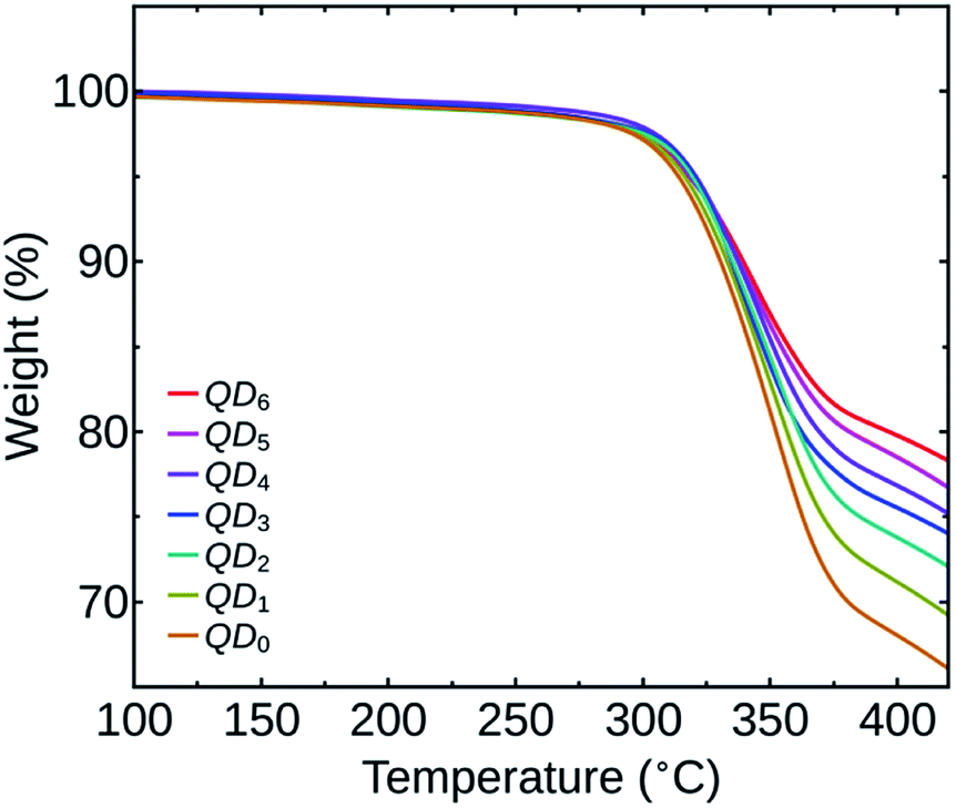
PbS QDs of about 3 nm size were synthesized for the study. The HR-TEM image of the nanocrystals confirming the size, crystallinity and monodispersity is shown in the ESI (Fig. S1†). The optical bandgap of the QDs was determined from the first excitonic peak (960 nm) in the optical absorption spectrum and was found to be 1.29 eV (Fig. S2 in the ESI†). We have prepared seven PbS QDs samples, numbered as QD0 to QD6 based on the number of washing cycles, as mentioned before.To quantify the variation in the amount of OA ligands on the QDs surface based on the number of washing cycles performed, we have carried out a TGA analysis of all the QDs samples. Fig. 1 shows the TGA spectra of the samples QD0 to QD6. The spectra show that the OA content on the QDs surface started decomposing at around 300 °C and from 400 °C onwards the curve takes a linear nature for all the samples. We have compared the relative weight loss of the QDs samples at 400 °C.
 | ||
| Fig. 1 TGA spectra of the QDs samples QD0 to QD6. | ||
For the sample QD0, the decomposition of the OA ligand resulted in a reduction of 32.0% of its initial weight and for the sample QD6, the observed weight loss was only 20.2%. As the number of washing cycles were increased, there was a reduction in the amount of OA on the QDs as indicated by a decrease in weight loss. The relative weight losses of the different samples (in percentage) are listed in Table 1.
| Sample name | Relative weight loss at 400 °C (in percentage) |
|---|---|
| QD0 | 32.0 |
| QD1 | 28.8 |
| QD2 | 26.2 |
| QD3 | 24.5 |
| QD4 | 23.2 |
| QD5 | 21.5 |
| QD6 | 20.2 |
We can also observe that the relative decrease in the amount of OA is significantly higher between the initial washing cycles. The initial weight loss is attributed to the removal of weakly adsorbed OA ligands on the QDs surface during washing.14 The remaining strongly bound OA ligands attached as Pb-oleates in the QDs are less susceptible to further washing, resulting in a reduced ligand loss during the last numbers of washing cycles.
To appreciate the effect of the number of post-synthesis washing cycles on the QDs films, we fabricated QDs films having thickness around 40 nm using the seven QDs samples and were then ligand exchanged with TBAI. The films were grown on glass substrates and for TBAI exchange, they were treated with TBAI in ethanol and rinsed with ethanol thrice. Ethanol was used here because it is considered as a better solvent than the commonly used methanol. During the TBAI exchange, the intrusive nature of the methanol could result in unpassivated Pb sites leading to an increased trap state density deteriorating the overall device performance, as reported earlier.28 Some reports also suggests that rinsing with methanol could result in the removal of Pb atom along with OA as Pb-oleates inducing stoichiometric unbalance in the QDs,29 which can mislead the present investigation. Detailed film fabrication and ligand exchange procedures are provided in the experimental section. The TBAI treated films were named TBAI0, TBAI1, … and TBAI6 respectively, corresponding to the QDs samples QD0, QD1, … and QD6. The Cr-SEM images of the devices made with TBAI0 and TBAI6 are shown in Fig. 2, suggesting that the number of washing cycles has practically no effect on the PbS QDs film thickness.
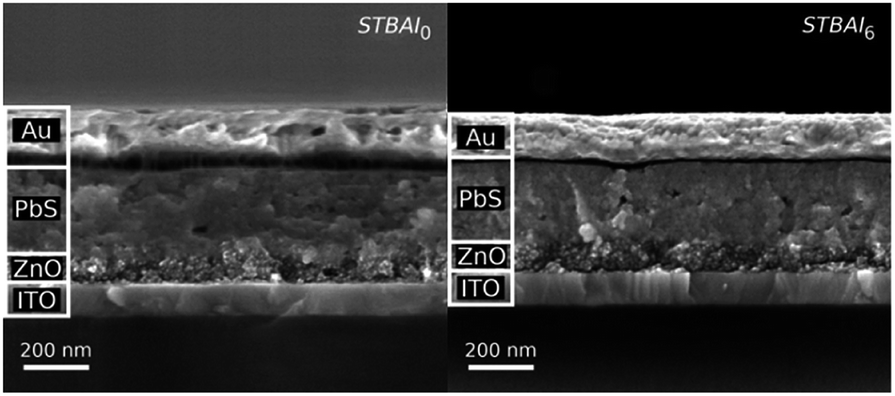 | ||
| Fig. 2 Cr-SEM images of the devices STBAI0 and STBAI6 (naming is introduced later in the manuscript). | ||
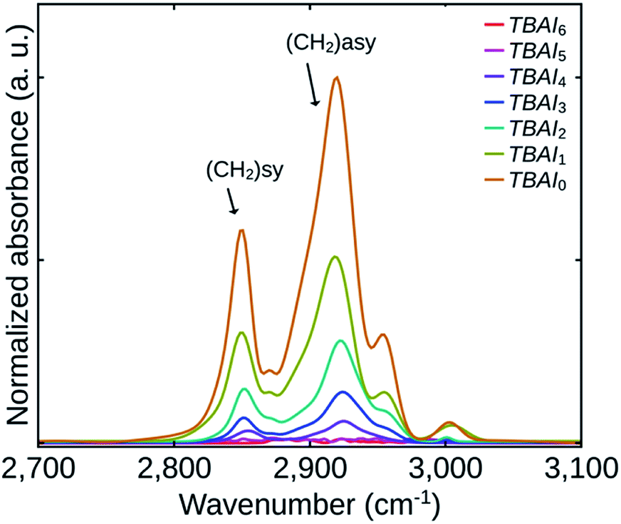
To get a quantitative estimate of the variation of the residual OA on the TBAI exchanged QDs in the films, FTIR analysis of all the films were done. Fig. 3 shows the FTIR spectra of the films indicating asymmetric (2920 cm−1) and symmetric stretching (2850 cm−1) vibrations of CH2 group of OA.18,19
 | ||
| Fig. 3 FTIR spectra of the samples TBAI0 to TBAI6. | ||
Since the QDs loading could be different for the TBAI exchanged films for the same thickness, the individual FTIR spectra were normalized with respect to the absorbance of first excitonic peak of the respective samples. The absorbances of the films depend on their QDs loading and its effect is evident from the absorption spectra shown in Fig. 4. The FTIR spectra demonstrates that the amount of residual OA was reducing in the films up to TBAI4 with the two samples TBAI5 and TBAI6 not showing any signs of OA. This means that in TBAI5 and TBAI6, the OA is totally replaced by TBAI in the ligand exchange process. Now correlating the FTIR results with the TGA data explained previously, we can confirm that the residual OA on the QDs films after the TBAI exchange is decided by the number of post-synthesis washing cycles carried out on the QDs samples. The observations are in close agreement with the previous reports on the ligand exchange using BDT.23 One can therefore conclude that, by suitably adjusting the OA component in the QDs with the number of washing cycles, we can control the residual OA on the TBAI treated films. The method appears to be efficient in making the TBAI exchange effective, a factor that is important in the performance of photovoltaic devices, which is discussed later in this manuscript.
 | ||
| Fig. 4 Absorption spectra of the samples TBAI0 to TBAI6. | ||
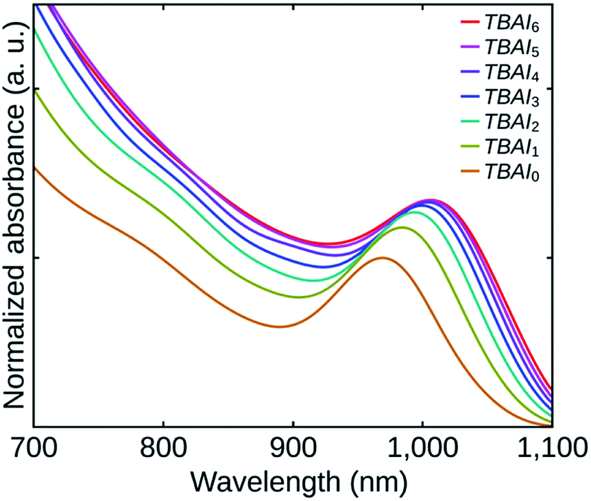
Fig. 4 shows the absorption spectra of the TBAI treated QDs films. Though the film thicknesses were practically the same, the absorbances of the films can be found to be increasing from TBAI0 to TBAI6 which can be attributed to an increase in the QDs packing density in the films (QDs loading effect). The removal of the OA through post-synthesis washing cycles and the following TBAI exchange make the QDs closer to each other, increasing the packing density of the films. Note that, the variation in absorbance (hence the packing density) is noticeable only in the initial samples and afterwards, the effects become feeble to differentiate. A significant red shift can also be observed with an increase in the number of washing cycles. This change is ascribed to the strengthened electronic coupling between the QDs, which in turn is related to the distance between the individual QDs in the films.30,31 The conductivity of the TBAI treated films is expected to increase with increase in the number of washing cycles, as it is directly related to the electronic coupling between the QDs.5,13,19,31,32 The results are also reflected in the performance of cell structures fabricated, which is discussed later in this paper.
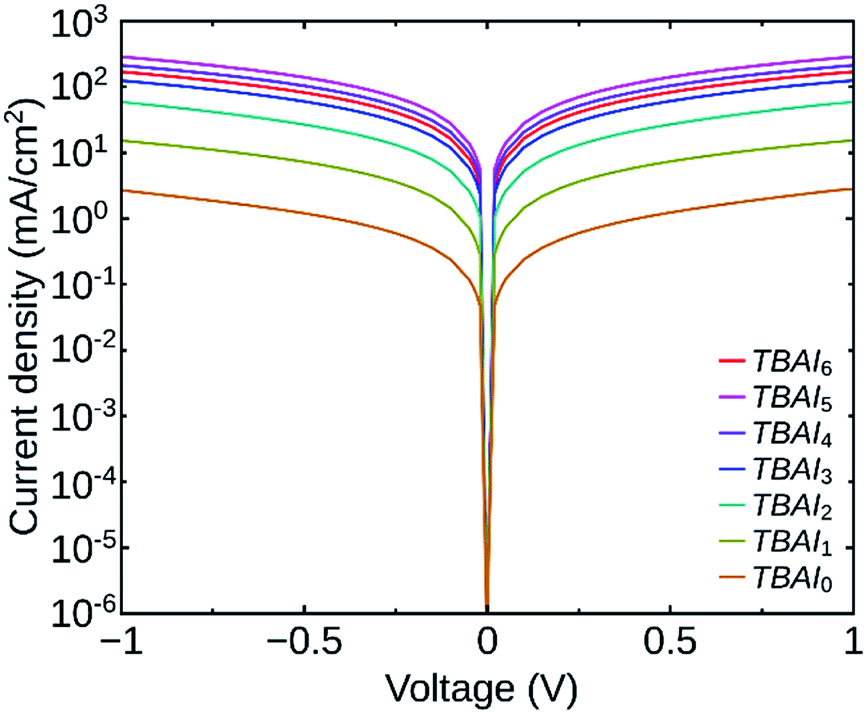
In order to investigate the impact of the number of washing cycles on the conductivity of the PbS QDs film, we have analysed the dark J–V characteristics of devices having the structure ITO/Au/PbS(TBAI)/Au. Fig. 5 shows the J–V curves of the devices having QDs with different number of washing cycles. We can see that the QDs film with minimum washing cycles (TBAI0) has the minimum conductivity (5.7 × 10⁻⁸ S cm−1) as expected and the conductivity increases up to TBAI5 (6.7 × 10⁻⁶ S cm−1). The trend reverses for TBAI6 (3.9 × 10⁻⁶ S cm−1) and its value is lower than that for TBAI5. It is clear that a higher number of washing cycles can lead to deterioration of the film quality.
 | ||
| Fig. 5 Dark J–V curves of the devices TBAI0 to TBAI6. | ||
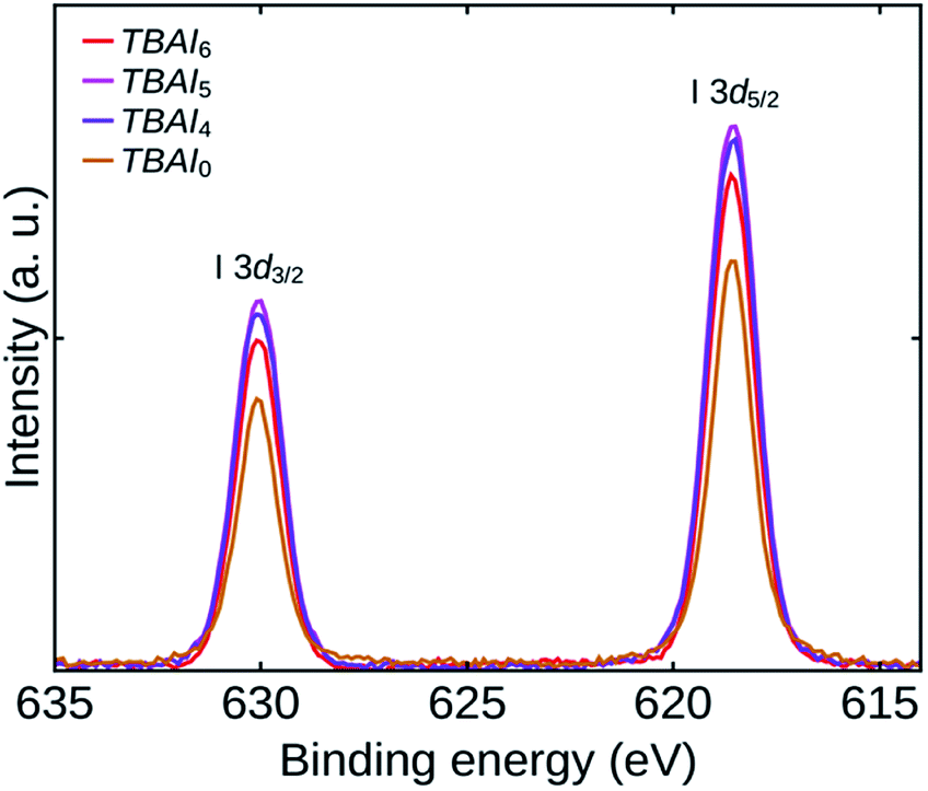
An XPS analysis was performed further to get a clear understanding of the degree of TBAI exchange with OA and the evolution of OH− and O− surface groups by the consecutive QDs washing cycles. The oxygen (OH− and O−) groups were reported as a major source of sub-bandgap trap states in PbS QDs.14 Now, for the analysis, the total peak areas of all the spectra were normalized with respect to the total Pb peak area of the corresponding samples. Also, to make the comparison easy, the signal peaks corresponding to iodine and oxygen were further normalized with respect to the I and COO− peaks of TBAI0.
The extent of iodine passivation on the TBAI exchanged QDs films can be verified by examining the I 3d core level spectra of the samples.20,33 Fig. 6 shows the high-resolution I 3d core level spectra of TBAI0, TBAI4, TBAI5, and TBAI6. The spectra show that the iodide passivation is increasing up to TBAI5 and afterwards it is showing a reverse trend. Combining this observation with the TGA results, we can conclude that the efficiency of the TBAI treatment is increasing with reduction in the amount of initial OA, which might be the result of diminished steric hindrance of the OA shell due to its reduced density on the QDs surface. Sargent group has already reported the steric hindrance effect of an initial ligand shell, which can prevent a complete replacement of it with iodide during a solid-state ligand exchange processes.1,15 A significant reduction in OA observed in FTIR with an increase in the number of washing cycles is a result of the reduction in initial OA and the increased ligand exchange efficiency. It has been found that the TBAI exchange has reached its maximum for TBAI5 and a lower iodine passivation for TBAI6 as it has already a lesser amount of initial OA than TBAI5, with the remaining sites occupied by the impurities (mostly oxygen groups). It was also seen that the TBAI was incapable in replacing the oxygen impurities attached to the QDs during solid-state ligand exchange process.
 | ||
| Fig. 6 High-resolution XPS I 3d core level spectra of the samples TBAI0, TBAI4, TBAI5 and TBAI6. | ||
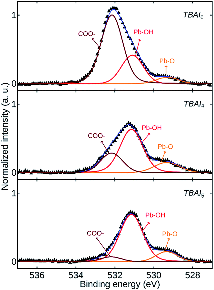
Fig. 7 shows the high-resolution O 1s core level spectra of TBAI0, TBAI4 and TBAI5. The spectra were deconvoluted to obtain the signals corresponding to the atomic groups present. The peak at 532.2 eV corresponds to the residual bound oleate (COO−) ligand or CO2. The second peak at 531.2 eV is associated with the hydroxyl (OH−) group bound on (111) surface facets of the QDs surface. The origin of this OH− is attributed to two possibilities. First one is the OH− residue from the synthesis procedure and the second one is caused by the moisture content in the ambient atmosphere during the ligand exchange and the further processes. The third peak at 529.3 eV is attributed to the oxygen related to Pb–O.20,33,34 The dominant COO− peak in TBAI0 is representative of the residual OA in the film, which is disappearing in TBAI5, complementing the FTIR results. Two of the other peaks ascribed to OH− and O− are increasing in intensity with an increase in the number of washing cycles. This occurs as a result of the attachment of the OH− and O- groups to the exposed unpassivated Pb sites due to the loss of OA ligands from the QDs as the result of QDs washing.
 | ||
| Fig. 7 High-resolution XPS O 1s core level spectra of the samples TBAI0, TBAI4 and TBAI5. | ||
Finally, to verify the effect of the number of washing cycles on photovoltaic device characteristics, we have fabricated planar heterojunction solar cells having the architecture ITO/ZnO/PbS(TBAI)/Au. The devices were made by coating six successive QDs layers, each having a thickness of around 40 nm. Fabrication procedures of the cell structures are discussed in detail in the experimental section. The devices were named as STBAI0, STBAI1, … and STBAI6 indicating their TBAI exchanged QDs layer. For comparison, we have also fabricated a reference device using TBAI0, having similar architecture and thickness, grown in eleven thin layers, using conventional techniques for ensuring complete TBAI exchange. The device was named STBAIr. The parameters, VOC, JSC, fill factor (FF), PCE, shunt resistance (RSH) and series resistance (RS) of all the devices are tabulated in Table 2. The values shown correspond to the average of three modules having eight cells each. The RS and RSH values were calculated at the open-circuit and short-circuit conditions respectively. Among all the devices fabricated, the device STBAI4 delivered the best performance. The J–V characteristics of the devices STBAI4 and STBAIr are shown in Fig. 8 and the same for the rest of the devices are provided in the ESI (Fig. S3†).
| Devices | VOC (V) | JSC (mA cm−2) | FF | Eff. (%) | RSH (Ω cm−2) | RS (Ω cm−2) |
|---|---|---|---|---|---|---|
| STBAI0 | 0.54 ± 0.01 | 13.3 ± 1.11 | 0.39 ± 0.01 | 2.80 ± 0.14 | 306.4 ± 12.5 | 14.1 ± 0.8 |
| STBAI1 | 0.53 ± 0.01 | 17.9 ± 1.19 | 0.44 ± 0.02 | 4.17 ± 0.17 | 247.8 ± 9.8 | 10.8 ± 1.0 |
| STBAI2 | 0.52 ± 0.01 | 19.7 ± 1.03 | 0.46 ± 0.01 | 4.71 ± 0.13 | 221.4 ± 13.5 | 8.2 ± 0.6 |
| STBAI3 | 0.51 ± 0.01 | 20.8 ± 1.25 | 0.46 ± 0.01 | 4.88 ± 0.15 | 200.4 ± 8.5 | 7.5 ± 0.7 |
| STBAI4 | 0.51 ± 0.01 | 22.3 ± 1.17 | 0.49 ± 0.01 | 5.55 ± 0.17 | 196.0 ± 8.9 | 6.9 ± 0.6 |
| STBAI5 | 0.49 ± 0.02 | 22.3 ± 1.37 | 0.48 ± 0.02 | 5.24 ± 0.18 | 183.5 ± 10.3 | 7.0 ± 0.8 |
| STBAI6 | 0.46 ± 0.04 | 21.6 ± 1.72 | 0.44 ± 0.02 | 4.36 ± 0.21 | 136.3 ± 11.5 | 6.8 ± 1.0 |
| STBAIr | 0.52 ± 0.01 | 21.1 ± 1.05 | 0.46 ± 0.01 | 5.07 ± 0.13 | 238.1 ± 9.3 | 10.5 ± 0.6 |
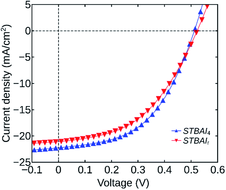 | ||
| Fig. 8 J–V characteristics of the devices STBAI4 and STBAIr. | ||
Table 2 shows that the JSC and FF values are increasing with the number of washing cycles carried out. We have already seen that the conclusions from TGA, FTIR and the absorption studies are illustrative of an increased electronic coupling between the QDs due to an improved QDs packing density.5,31,32 In addition, the conductivity study is also in agreement with the above observation. The improved charge transport properties are reflected by the enhancement of JSC and FF and a decrease in RS.
The VOC of the devices were found to be decreasing with an increase in the number of washing cycles. This can be attributed to an increase in the surface trap density originating from the attachment of OH− and O− species to the unpassivated Pb sites due to an increased removal of OA. The trap states can act as recombination centres increasing the photo-current leakage.14 A reduction of RSH with an increase in the number of washing cycles is in line with the VOC decrease related to the increased charge recombination through surface states caused by the excess ligand loss.
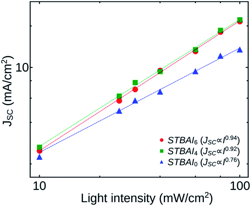
For a clear understanding of the recombination kinetics in the devices fabricated, we analysed how JSC and VOC depend on the light intensity I. Fig. 9 shows the dependence of JSC on I of the devices STBAI0, STBAI4 and STBAI6. The curves were plotted on a double logarithmic scale and were then fitted with a power-law based on the proportionality JSC ∝ Iγ, where γ is an exponential factor, the value of which can be used to identify the carrier recombination mechanism in the devices under short-circuit condition. A γ value close to 1 indicates that the carrier extraction is faster than recombination in a device so that it exhibits very little bimolecular recombination under short-circuit condition or the device may be dominated by monomolecular (trap-assisted) recombination. A lower value of γ (∼0.5) is suggestive of bimolecular recombination processes in the device under consideration.35 In our study, the γ values obtained for the devices STBAI0, STBAI4 and STBAI6 are 0.76, 0.92 and 0.94, respectively. A comparatively lower value of γ in STBAI0 shows that the device possesses a noticeable bimolecular recombination of accumulated charge carriers due to the poor charge extraction caused by the residual OA. In STBAI4 and STBAI6, the photocurrent was determined by the electron–hole pair generation by the photon absorption with a few bimolecular recombination at short-circuit conditions.36,37
 | ||
| Fig. 9 Dependence of JSC on light intensity for the devices STBAI0, STBAI4 and STBAI6. | ||
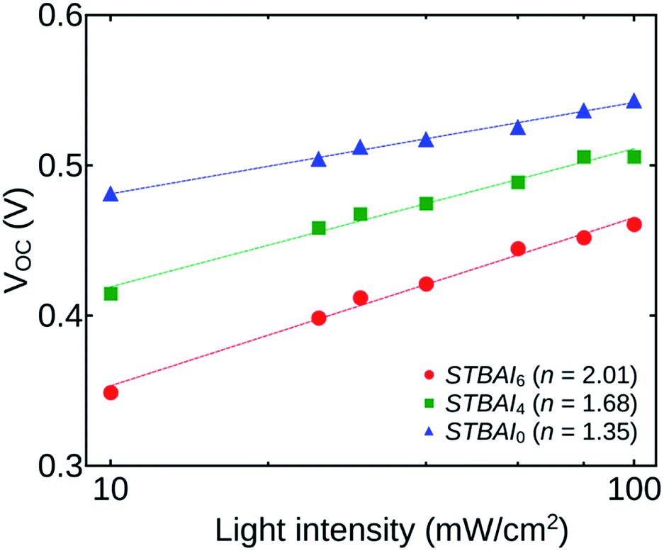
To proceed further, we have calculated the diode ideality factors n for the devices STBAI0, STBAI4 and STBAI6. The value of ideality factor is an indicator of the dominant recombination mechanism in a cell under consideration. One of the methods to obtain the value of n is by fitting the ideal diode equation to the J–V curve under dark. But, the method is less adopted due to the complications in avoiding the effect of series resistance and the lack of a well-defined slope at the low forward bias for an exact calculation of the n value.37,38 In our study, we have calculated the ideality factor by studying the dependence of VOC on light intensity. When the measurements are carried out at open-circuit conditions, the effect of series resistance on the ideality factor can be ruled out.
Fig. 10 shows the light intensity dependence of VOC for the devices STBAI0, STBAI4 and STBAI6 plotted on a logarithmic scale. The ideality factor can be obtained by fitting the data using the relation VOC = (nkT/q)ln(Iγ) + C, where, k is the Boltzmann constant, T is the absolute temperature, q is the elementary charge, γ is the exponential factor determined from the JSC versus I study and C is a constant. The ideality factor gives a value 1 when there is only band-to-band bi-molecular recombination in the open-circuit condition. The value will be in the range between 1 and 2 when the trap assisted recombination from mid-gap states dominates.36,37 The ideality factor determined for STBAI0, STBAI4 and STBAI6 are 1.35, 1.68 and 2.01, respectively. An increase of n shows that the contribution from trap assisted recombination is increasing with the number of washing cycles. The effects are mainly sourced from the OH− and O− groups getting attached to the OA free regions.
 | ||
| Fig. 10 Dependence of VOC on light intensity for the devices STBAI0, STBAI4 and STBAI6. | ||
The discussions carried out so far can be summarized using a schematic shown in Fig. 11. By increasing the number of washing cycles, the OA ligand density of the QDs is reduced along with the creation of OH− and O− trap states. A reduction in the density of OA on the QDs films has been found to be enhancing the ligand exchange efficiency and reducing the residual OA in the films. The QDs films fabricated from a minimum number of washing cycles have very poor QDs packing density and transport properties, but their efficient surface passivation by either iodine or OA makes them less susceptible to the trap generating impurities (OH−/O−). This means that the trap states density of the devices grown from these films is low, providing them a higher VOC. However, their PCE is small due to higher RS and lower JSC and FF. On increasing the number of washing cycles, charge transport properties of the QDs films improved along with an increase in trap density. Of the eight devices fabricated, the device corresponding to four washing cycles (STBAI4) was found to be optimal in terms of the PCE. A significant loss of OA from QD5 and QD6 has resulted in an appreciable increase of traps states in STBAI5 and STBAI6 resulting in lower values of RSH and VOC in these devices.
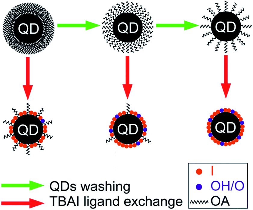 | ||
| Fig. 11 Schematic representation of the washing and ligand exchange effect. | ||
Conclusions
We have comprehensively investigated the role of post-synthesis washing cycles on OA capped PbS QDs which are subjected to a solid-state ligand exchange process with TBAI and the performance of cell structures fabricated. It was found that the amount of residual OA after the solid-state ligand exchange was directly related to the amount of initial OA on the QDs surface and this could be controlled through post-synthesis washing cycles. Also, the ligand exchange efficiency was enhanced with a reduction in the OA on the QDs surface prior to the ligand exchange. The number of washing cycles on the QDs was varied progressively from one to six using systematic procedures and the films grown from them were subjected to an exchange with TBAI. An optimized photovoltaic performance of 5.55% was achieved in the sample that has undergone four washing cycles. Apart from the above finding, our study also introduces a well-organized approach for ensuring a complete TBAI exchange of thicker QDs films, which indeed makes the device fabrication much easier.Conflicts of interest
There are no conflicts to declare.Acknowledgements
The corresponding author V. V. Ison gratefully acknowledges SERB, DST, Govt. of India, for an earlier fast track project (Order No. SR/FTP/PS-108/2010). The authors thank Dr Biju P. R., Associate Professor, School of Pure and Applied Physics, Mahatma Gandhi University, Kottayam for his support during the solar cell fabrications.References
- M. Yuan, M. Liu and E. H. Sargent, Nat. Energy, 2016, 1(3), 1–9 CrossRef.
- G. H. Carey, A. L. Abdelhady, Z. Ning, S. M. Thon, O. M. Bakr and E. H. Sargent, Chem. Rev., 2015, 115(23), 12732–12763 CrossRef CAS PubMed.
- O. E. Semonin, J. M. Lutherand and M. C. Beard, Mater. Today, 2012, 15(11), 508–515 CrossRef CAS.
- O. E. Semonin, J. M. Luther, S. Choi, H. Y. Chen, J. Gao, A. J. Nozik and M. C. Beard, Science, 2011, 334(6062), 1530–1533 CrossRef CAS PubMed.
- J. Xu, O. Voznyy, M. Liu, A. R. Kirmani, G. Walters, R. Munir, M. Abdelsamie, A. H. Proppe, A. Sarkar, F. P. G. de Arquer and M. Wei, Nat. Nanotechnol., 2018, 13(6), 456–462 CrossRef CAS PubMed.
- J. Y. Kim, O. Voznyy, D. Zhitomirsky and E. H. Sargent, Adv. Mater., 2015, 27(26), 3849 CrossRef CAS PubMed.
- X. Lan, O. Voznyy, F. P. G. de Arquer, M. Liu, J. Xu, A. H. Proppe, G. Walters, F. Fan, H. Tan, M. Liu and Z. Yang, Nano Lett., 2016, 16(7), 4630–4634 CrossRef CAS PubMed.
- G. W. Hwang, D. Kim, J. M. Cordero, M. W. Wilson, C. H. M. Chuang, J. C. Grossman and M. G. Bawendi, Adv. Mater., 2015, 27(30), 4481–4486 CrossRef CAS PubMed.
- L. Hu, S. Huang, R. Patterson and J. E. Halpert, J. Mater. Chem. C, 2019, 7(15), 4497–4502 RSC.
- P. N. Goswami, D. Mandal and A. K. Rath, Nanoscale, 2018, 10(3), 1072–1080 RSC.
- R. W. Crisp, D. M. Kroupa, A. R. Marshall, E. M. Miller, J. Zhang, M. C. Beard and J. M. Luther, Sci. Rep., 2015, 5, 9945 CrossRef CAS PubMed.
- J. Tang, K. W. Kemp, S. Hoogland, K. S. Jeong, H. Liu, L. Levina, M. Furukawa, X. Wang, R. Debnath, D. Cha and K. W. Chou, Nat. Mater., 2011, 10(10), 765–771 CrossRef CAS PubMed.
- C. H. M. Chuang, P. R. Brown, V. Bulovic and M. G. Bawendi, Nat. Mater., 2014, 13(8), 796–801 CrossRef CAS PubMed.
- Y. Cao, A. Stavrinadis, T. Lasanta, D. So and G. Konstantatos, Nat. Energy, 2016, 1(4), 1–6 Search PubMed.
- Z. Ning, Y. Ren, S. Hoogland, O. Voznyy, L. Levina, P. Stadler, X. Lan, D. Zhitomirsky and E. H. Sargent, Adv. Mater., 2012, 24(47), 6295–6299 CrossRef CAS PubMed.
- H. Wei, D. Li, X. Zheng and Q. Meng, Chin. Phys. B, 2018, 27(1), 018808 CrossRef.
- D. M. Balazs, D. N. Dirin, H. H. Fang, L. Protesescu, G. H. ten Brink, B. J. Kooi, M. V. Kovalenko and M. A. Loi, ACS Nano, 2015, 9(12), 11951–11959 CrossRef CAS PubMed.
- J. Hong, B. Hou, J. Lim, S. Pak, B. S. Kim, Y. Cho, J. Lee, Y. W. Lee, P. Giraud, S. Lee and J. B. Park, J. Mater. Chem. A, 2016, 4(48), 18769–18775 RSC.
- B. S. Kim, J. Hong, B. Hou, Y. Cho, J. I. Sohn, S. Cha and J. M. Kim, Appl. Phys. Lett., 2016, 109(6), 063901 CrossRef.
- R. Azmi, S. Sinaga, H. Aqoma, G. Seo, T. K. Ahn, M. Park, S. Y. Ju, J. W. Lee, T. W. Kim, S. H. Oh and S. Y. Jang, Nano Energy, 2017, 39, 86–94 CrossRef CAS.
- J. M. Luther, M. Law, Q. Song, C. L. Perkins, M. C. Beard and A. J. Nozik, ACS Nano, 2008, 2(2), 271–280 CrossRef CAS PubMed.
- M. H. Zarghami, Y. Liu, M. Gibbs, E. Gebremichael, C. Webster and M. Law, ACS Nano, 2010, 4(4), 2475–2485 CrossRef CAS PubMed.
- C. Piliego, L. Protesescu, S. Z. Bisri, M. V. Kovalenko and M. A. Loi, Energy Environ. Sci., 2013, 6(10), 3054–3059 RSC.
- A. Thomas, R. Vinayakan and V. V. Ison, RSC Adv., 2020, 10(28), 16693–16699 RSC.
- B. Hou, Y. Cho, B. S. Kim, J. Hong, J. B. Park, S. J. Ahn, J. I. Sohn, S. Cha and J. M. Kim, ACS Energy Lett., 2016, 1(4), 834–839 CrossRef CAS PubMed.
- D. K. Ko, A. Maurano, S. K. Suh, D. Kim, G. W. Hwang, J. C. Grossman, V. Bulovic and M. G. Bawendi, ACS Nano, 2016, 10(3), 3382–3388 CrossRef CAS PubMed.
- B. Shakeri and R. W. Meulenberg, Langmuir, 2015, 31(49), 13433–13440 CrossRef CAS PubMed.
- A. Hassinen, I. Moreels, K. De Nolf, P. F. Smet, J. C. Martins and Z. Hens, J. Am. Chem. Soc., 2012, 134(51), 20705–20712 CrossRef CAS PubMed.
- J. H. Song, H. Choi, Y. H. Kim and S. Jeong, Adv. Energy Mater., 2017, 7(15), 1700301 CrossRef.
- J. J. Choi, J. Luria, B. R. Hyun, A. C. Bartnik, L. Sun, Y. F. Lim, J. A. Marohn, F. W. Wise and T. Hanrath, Nano Lett., 2010, 10(5), 1805–1811 CrossRef CAS PubMed.
- M. Liu, O. Voznyy, R. Sabatini, F. P. G. de Arquer, R. Munir, A. H. Balawi, X. Lan, F. Fan, G. Walters, A. R. Kirmani and S. Hoogland, Nat. Mater., 2017, 16(2), 258–263 CrossRef CAS PubMed.
- K. J. Williams, W. A. Tisdale, K. S. Leschkies, G. Haugstad, D. J. Norris, E. S. Aydil and X. Y. Zhu, ACS Nano, 2009, 3(6), 1532–1538 CrossRef CAS PubMed.
- Y. Wang, K. Lu, L. Han, Z. Liu, G. Shi, H. Fang, S. Chen, T. Wu, F. Yang, M. Gu and S. Zhou, Adv. Mater., 2018, 30(16), 1704871 CrossRef PubMed.
- X. Yang, J. Yang, J. Khan, H. Deng, S. Yuan, J. Zhang, Y. Xia, F. Deng, X. Zhou, F. Umar, Z. Jin, H. Song, C. Cheng, M. Sabry and J. Tang, Nano-Micro Lett., 2020, 12(1), 37 CrossRef.
- D. Lee, J. Lim, M. Park, J. Y. Kim, J. Song, J. Kwak, S. Lee, K. Char and C. Lee, Nanotechnology, 2015, 26(46), 465401 CrossRef PubMed.
- Z. Sun, G. Sitbon, T. Pons, A. A. Bakulin and Z. Chen, Sci. Rep., 2015, 5, 10626 CrossRef PubMed.
- M. J. Speirs, D. M. Balazs, H. H. Fang, L. H. Lai, L. Protesescu, M. V. Kovalenko and M. A. Loi, J. Mater. Chem. A, 2015, 3(4), 1450–1457 RSC.
- C. Ding, Y. Zhang, F. Liu, N. Nakazawa, Q. Huang, S. Hayase, Y. Ogomi, T. Toyoda, R. Wang and Q. Shen, ACS Appl. Mater. Interfaces, 2017, 10(31), 26142–26152 CrossRef PubMed.
Footnote |
| † Electronic supplementary information (ESI) available. See DOI: 10.1039/d0ra05242f |
| This journal is © The Royal Society of Chemistry 2020 |