
 Open Access Article
 This Open Access Article is licensed under a Creative Commons Attribution-Non Commercial 3.0 Unported Licence
Resistance state evolution under constant electric stress on a MoS2 non-volatile resistive switching device†
Xiaohan Wu ,
Ruijing Ge,
Yifu Huang,
Deji Akinwande and
Jack C. Lee
,
Ruijing Ge,
Yifu Huang,
Deji Akinwande and
Jack C. Lee
Microelectronics Research Center, The University of Texas at Austin, Austin, Texas 78758, USA. E-mail: leejc@austin.utexas.edu; deji@ece.utexas.edu
First published on 19th November 2020
Abstract
MoS2 has been reported to exhibit a resistive switching phenomenon in a vertical metal–insulator–metal (MIM) structure and has attracted much attention due to its ultra-thin active layer thickness. Here, the resistance evolutions in the high resistance state (HRS) and low resistance state (LRS) are investigated under constant voltage stress (CVS) or constant current stress (CCS) on MoS2 resistive switching devices. Interestingly, compared with bulk transition metal oxides (TMO), MoS2 exhibits an opposite characteristic in the fresh or pre-RESET device in the “HRS” wherein the resistance will increase to an even higher resistance after applying CVS, a unique phenomenon only accessible in 2D-based resistive switching devices. It is inferred that instead of in the highest resistance state, the fresh or pre-RESET devices are in an intermediate state with a small amount of Au embedded in the MoS2 film. Inspired by the capability of both bipolar and unipolar operation, positive and negative CVS measurements are performed and show similar characteristics. In addition, it is observed that the resistance state transition is faster when using higher electric stress. Numerical simulations have been performed to study the temperature effect with small-area integration capability. These results can be explained by a modified conductive-bridge-like model based on Au migration, uncovering the switching mechanisms in the ultrathin 2D materials and inspiring future studies in this area.
1 Introduction
In the last few years, various two-dimensional (2D) materials have been reported to exhibit non-volatile resistive switching (NVRS) behavior including functionalized graphene oxide, degraded black phosphorus, double-layer MoS2, single- or multi-layer hexagonal boron nitride (h-BN), etc.1–6 These devices, in the simple structure of metal–insulator–metal (MIM), are based on the resistive switching effect in the active layer, where the resistance can be repeatably switched between a high resistance state (HRS) and a low resistance state (LRS) and sustained without any power supply.7–11 Compared with the transition metal oxide (TMO)-based resistive random access memory (RRAM), the 2D-based NVRS devices have drawn much attention due to the atomically thin active layer thickness, the complex switching mechanisms involving interaction of defects and ions at the sharp interfaces, and the potential applications in flexible memory fabrics and neuromorphic computing.12–15 In 2018, the “atomristors” based on monolayer or few-layer transition metal dichalcogenides (TMDs), was first demonstrated in vertical MIM configuration and show stable NVRS behavior with high ON/OFF ratio, fast switching speed and forming-free characteristics.16–19Constant electric stress has been used in RRAM devices with bulk metal oxides as active layers to study transition time, reliability and switching mechanisms.20–24 In this article, we performed constant voltage stress (CVS) and constant current stress (CCS) on MoS2-based NVRS devices. It has been found that for fresh devices or working devices that RESET to HRS, the resistance would increase to an even higher resistance state by applying CVS at low voltages, instead of decreasing to LRS in conventional metal-oxide memory devices. To the best of our knowledge, this unique phenomenon has only been reported for the 2D-based NVRS devices, indicating a distinct switching mechanism due to the ultrathin active layer thickness. While with CVS at higher voltage (>SET voltage), the devices will be switched to LRS. This observation implies that the initial state or the “HRS” obtained by voltage sweeping is not the highest resistance state, but an intermediate state. Both positive and negative CVS were applied on the pre-RESET devices, showing similar resistance increasing behavior, which is consistent with the co-existence of bipolar and unipolar modes in MoS2 atomristors. On the other hand, by using CCS on the devices at HRS, the resistance will be switched to a LRS. The different behaviors under current and voltage stress suggest that SET process is triggered by electric field, while RESET process is dominated by Joule heating. In addition, we performed CVS and CCS on working devices at LRS to switch them to HRS. It is also observed that with higher electric stress, the resistance state transition time will be shorter. To study the Joule heating effect during RESET process, we have performed numerical simulations and demonstrated significant temperature reduction using diamond substrate, enabling small-area device integration. The electric stress test results provide evidence for the switching mechanisms in MoS2 atomristors which can be explained by a modified conductive-bridge-like model with Au ion migration to interpret the conductive path evolution.
2 Device fabrication and characterization
The CVD-grown continuous 3–5 layers MoS2 films on SiO2/Si substrate were purchased from SixCarbon Technology. Bottom electrodes (BE) were patterned by electron beam lithography and deposited with a 2 nm Cr/100 nm Au metal stack by electron beam evaporation on a commercial diamond substrate. The MoS2 layer was transferred onto the target substrate with BE using a polydimethylsiloxane (PDMS) stamp transfer method.16 The PDMS stamp was adhered to the MoS2 film and then the sample was soaked into diluted water. The MoS2–PDMS film was separated from the hydrophilic SiO2/Si substrate and brought into contact with the target diamond substrate. The PDMS was subsequently peeled off, leaving the continuous MoS2 film (∼2 × 2 mm2) on the target substrate with BE on it. The crossbar devices were finished by the patterning and deposition of top electrodes (TE) using the same method as BE. Au was used as both BE and TE to avoid metal oxide formation. The fabricated devices were measured on a Cascade probe station with an Agilent 4156 semiconductor analyzer under ambient conditions. Raman spectroscopy was performed to evaluate the MoS2 film by a Renishaw inVia system using a 532 nm wavelength source.3 Results and discussions
The schematic and optical image of fabricated crossbar device are shown in Fig. 1a and b respectively. The vertical MIM device structure consists of a 3–5 layers MoS2 film and two gold electrodes. The device area (typically 0.5 × 0.5 μm2 in this paper) is defined as the overlapped region between TE and BE. Compared with SiO2/Si substrate with a low thermal conductivity for SiO2 (1.4 W m−1 K−1), diamond substrate is used in the MoS2-based memory devices with a high thermal conductivity of ∼1000 W m−1 K−1 that can dissipate the excessive heat through the substrate more effectively. This prevents the narrow metal electrode lines from Joule heating and thus enables the fabrication of small-area crossbar devices. Raman spectroscopy was performed and displayed in Fig. 1c, showing high quality of the crystalline 2D layered material.25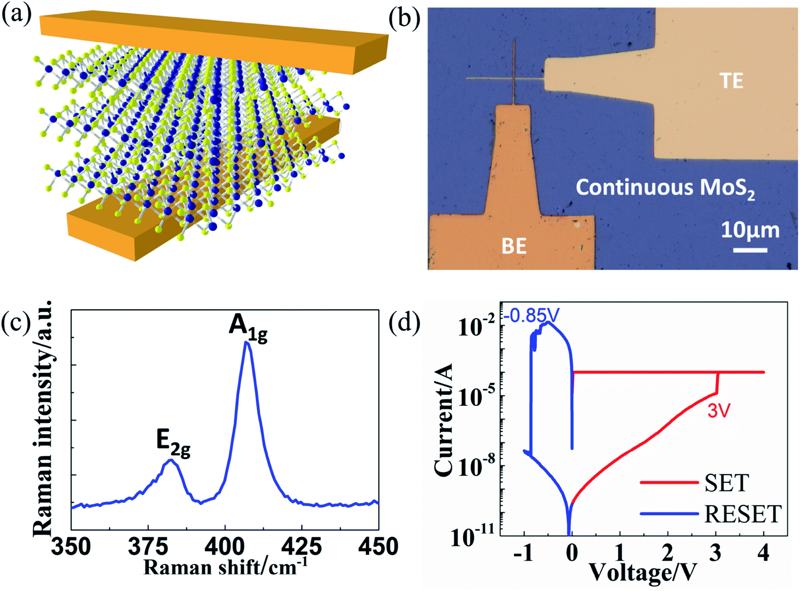 | ||
| Fig. 1 Device characterization and basic switching curve. (a) The schematic of crossbar device with few-layer MoS2 as the active layer. (b) The optical image of fabricated crossbar device with continuous MoS2 layer sandwiched between Au electrodes on diamond substrate. The area of this device is 0.5 × 0.5 μm2. (c) Raman spectrum of CVD-grown 3–5 layers MoS2 film. (d) A representative I–V curve of MoS2 resistive switching device. The SET and RESET voltage are 3 V and −0.85 V respectively. | ||
Fig. 1d shows a representative bipolar I–V switching curve of a crossbar MoS2 NVRS device. At first, the as-fabricated devices are generally at HRS. By applying a positive voltage bias, the current suddenly increases to the compliance, indicating a transition from HRS to LRS (“SET” process). The reverse transition (“RESET” process) is realized by applying a negative voltage sweep (bipolar mode) or a positive voltage sweep (unipolar mode), which are both accessible for MoS2 NVRS devices.16 The critical voltages that trigger the resistive switching behavior are called SET and RESET voltage. Note that a high RESET current is commonly observed in both traditional bulk oxide-based and emerging 2D-based NVRS devices, which produces Joule heating in the switching layer that is responsible for the RESET process.2,7,26–28 In addition to voltage sweeping, other operation methods like current sweeping, pulse operation and constant electric stress including CVS and CCS as discussed below, can be used to study the switching characteristics and investigate the underlying mechanisms.
Fig. 2 shows the resistance evolution under CVS measured on the devices at HRS. The working devices that exhibit stable switching characteristics are tested for several DC cycles and RESET to HRS before stress measurement. Subsequently, relatively low constant voltage bias (<VSET) is applied on the devices as shown in Fig. 2a with positive CVS and Fig. 2b with negative CVS. It is observed that the resistance changes from HRS to an even higher resistance state (labelled as HRS′). This is opposite to the observation in the devices using bulk metal oxides as active layer, where the resistance is switched from HRS to LRS under CVS.22,24 The READ I–V curves before and after CVS in Fig. S1† clearly show the transition from HRS to HRS′ and demonstrate that this resistance state transition can be sustained without external stress. Similar behavior is observed with both positive and negative CVS, which can be associated with the co-existence of unipolar and bipolar modes in MoS2 NVRS devices. In addition, CVS test is performed on the fresh (as-fabricated) devices, showing similar HRS to HRS′ transition (see Fig. 2c). This phenomenon indicates that for both fresh devices and pre-RESET working devices, the commonly called “HRS” is not the highest resistance, but an intermediate state that can still be switched to a higher resistance state (HRS′). On the other hand, if the voltage stress is higher than the SET voltage (see Fig. 2d), the device will switch to LRS and then fail due to high power.
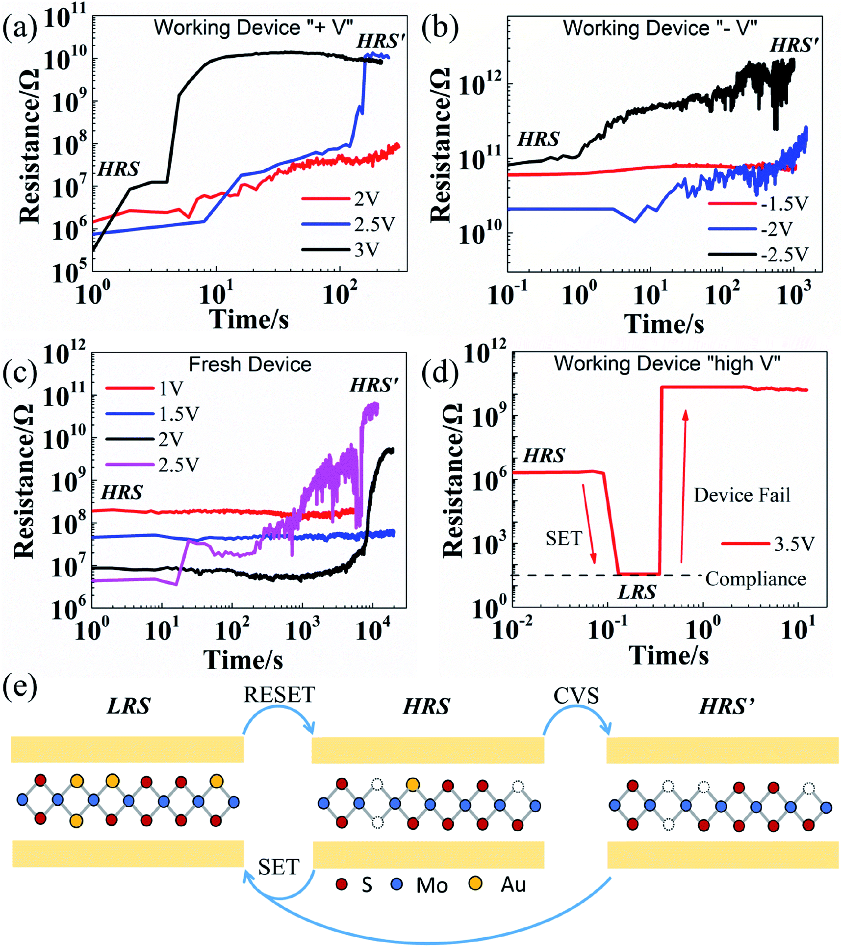 | ||
| Fig. 2 Resistance evolution under CVS for devices at HRS. The resistance of working devices at HRS (pre-RESET devices) measured during (a) positive voltage stress and (b) negative voltage stress. (c) The resistance of fresh (as-fabricated) devices at HRS measured during CVS. The resistance states change from HRS to a higher resistance state (labelled as HRS′) for the cases of (a)–(c). (d) The resistance of working devices at HRS measured during a high voltage stress (>VSET). The resistance state changes from HRS to LRS and then fails due to high power. (e) Illustration of the resistance states for MoS2 NVRS devices by voltage-sweep SET/RESET and low-voltage CVS. | ||
A previously proposed conductive-bridge-like model with the assistance of metal atom/ion migration is used to explain the NVRS phenomenon in MoS2 atomristors.4,17 The CVS test results provide more insights to the model with the resistance states illustrated in Fig. 2e. In MoS2 film, sulfur vacancies commonly exist and play an important role in resistive switching.29,30 The SET process is driven by the migration of Au ions into the sulfur vacancies, which changes the MoS2 film from semiconducting to metallic at the localized defect-rich regions. This atomic-level conductive-bridge-like model is supported by our recent finding that the Au atoms moving in and out from the vacancy site was directly observed by scanning tunnelling microscopy (STM), which results in NVRS behavior tested by electrical measurements using STM tip as the top electrode.31 The existence of HRS′ indicates that, a small amount of metal atoms may be embedded in the MoS2 film at HRS, which are possibly induced by deposition process for fresh devices or incomplete voltage-sweep RESET for working devices. Experimental evidence in supporting this proposed mechanism can be found in previous reports which suggest that metal atoms could diffuse into the defects in 2D TMD films during the evaporation deposition process of top electrodes as shown in cross-sectional TEM images.32,33 These embedded metal atoms/ions are negligible in bulk metal oxides, but are important in the atomically thin MoS2 sheets.7,34,35 With a relatively low voltage stress, these metal atoms tend to move out of the vacancies due to the accumulated Joule heating effect, resulting in a transition to the higher resistance state (HRS′). By applying a high voltage stress (>VSET), the sulfur vacancies would be substituted by more metal ions from the electrodes. This is similar to the SET process supported by ab initio simulation and STM measurements that one or multiple conductive links are formed.4,17,31 It is worth noting that the devices at HRS′ after CVS can still SET to LRS by voltage sweeping (see Fig. S2 in ESI†). It can be inferred from the CVS analysis that the SET process is dominated by electric field (voltage) since a voltage bias beyond the critical voltage is needed to trigger the resistance switching effect. The unique resistance evolution phenomenon under CVS treatment suggests a distinct property for 2D materials. For traditional bulk materials, the resistance state is typically determined by the characteristics of the conductive filament and the “gap” region between the electrode and filament tip.7,28 While for 2D materials, the resistance state can be modulated by the interaction between atoms/ions from electrodes and interfacial vacancies, which in turn enabling atomic-level resistance control with advanced defect engineering for crystalline 2D materials.
The resistance evolution under CVS measured on the devices at LRS is shown in Fig. 3. It is observed that the resistance states can be switched from LRS to HRS with either positive bias (Fig. 3a) or negative bias (Fig. 3b). The READ I–V curves before and after CVS are included in Fig. S3.† As shown in Fig. 3b as an example, with relatively low stress at −0.5 V, the device tends to remain at LRS. However, by applying higher voltage stress (at −0.75 V and −1 V), the device can be switched to HRS in a short time. This RESET-like behavior can be explained by the Joule heating induced by the high current (typically ∼10 mA) that dissolves the conductive path into metal ions, which then migrate back to the electrodes by reduction. Our previous experimental observation of co-existence of both bipolar and unipolar switching in MoS2-based devices provides additional evidence supporting this theory.7,28
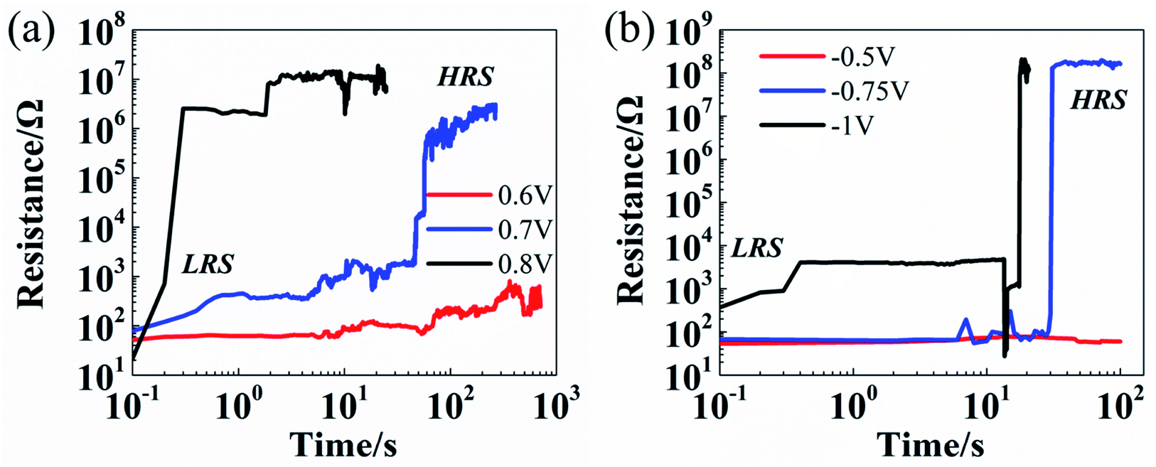 | ||
| Fig. 3 Resistance evolution under CVS for devices at LRS. The resistance of working devices at LRS (pre-SET devices) measured during (a) positive voltage stress and (b) negative voltage stress. The resistance states change from LRS to HRS for the cases of (a) and (b). | ||
CCS tests are performed on MoS2 NVRS devices and exhibit similar characteristics compared with traditional metal oxide-based devices.21–23 In Fig. 4a, CCS is applied on the devices at HRS, resulting in a resistance decrease from HRS to LRS, which can be attributed to the additional defects introduced into the MoS2 thin film under the low current stress. With relatively low current stress at 75 nA, the device stays at the initial HRS. While with higher stress (100 nA and 125 nA), the HRS-to-LRS transition can be observed shortly. Note that the current density here (up to 5 × 10⁵ A m−2) through the device is within the common range for NVRS devices at HRS.2,26,27,36,37 The READ I–V curves before and after CCS can be seen in Fig. S4,† showing the resistance transition from HRS to LRS can be maintained without external stress. For the devices at LRS (Fig. 4b), a transition from LRS to HRS happens under high CCS and then the device fails due to the high power. It is also observed that, the LRS-to-HRS transition, as shown in Fig. 3a, b and 4b, is a fast process with sudden resistance increase, which is similar to the sharp RESET behavior in voltage sweeping that caused by the conductive path rupture due to Joule heating. For all the electric stress tests, different stress amplitudes have been used, showing a common trend that higher electric stress results in shorter transition time.
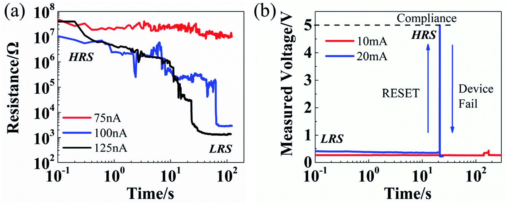 | ||
| Fig. 4 Resistance evolution under CCS for devices at HRS and LRS. (a) The resistance of devices at HRS measured during CCS. The resistance states change from HRS to LRS. (b) The voltage of devices at LRS measured during CCS. Resistance state changes from LRS to HRS with 20 mA CCS and then fails due to high power. | ||
To further study the Joule heating effect, numerical simulation has been performed to calculate the temperature distribution on MoS2-based devices during the RESET process. The electrical current and heat transfer in solids modules in COMSOL Multiphysics® are utilized to compute the Joule heat induced by electric current. In this model, a vertical metal–insulator–metal (MIM) structure is established on a SiO2/Si or diamond substrate (Fig. 5a). Crossbar device configuration is used with Au as TE/BE and continuous MoS2 film as the active layer. At LRS, a metallic cylinder with a radius of 50 nm is modelled as the conductive link. A voltage sweeping (0–2 V) is applied on TE while BE and substrate are grounded. Fig. 5b shows the peak temperature with different device area (from 0.5 × 0.5 μm2 to from 10 × 10 μm2). As the device area shrinks, the peak temperature increases. This is to be expected as the resistance of the metal line increases. This trend is consistent with the experimental observation that for devices below 1 × 1 μm2 on SiO2/Si substrate, the metal lines could actually be burned (or blown out) due to the high temperature induced by Joule heating effect. While by using diamond substrate with a high thermal conductivity, the peak temperature of a 0.5 × 0.5 μm2 device can be significantly reduced from 1558 °C on SiO2/Si substrate to 906 °C on diamond substrate, below Au melting point at 1064 °C. The calculated temperature distribution in Fig. 5c shows that the peak temperature region spreads to metal lines for the device on SiO2/Si substrate, resulting in the line burning phenomenon. As shown in Fig. 5d, benefiting from the high thermal conductivity of diamond substrate, the peak temperature region is confined within the device area. These simulations results, correlated with experimental data, demonstrate a significant temperature reduction during RESET process by using a diamond substrate, which prevents metal lines from burning and enables small-area device integration. Our simulation and experimental results provide additional insights into the failure analysis and mechanism studies due to Joule heating effect.
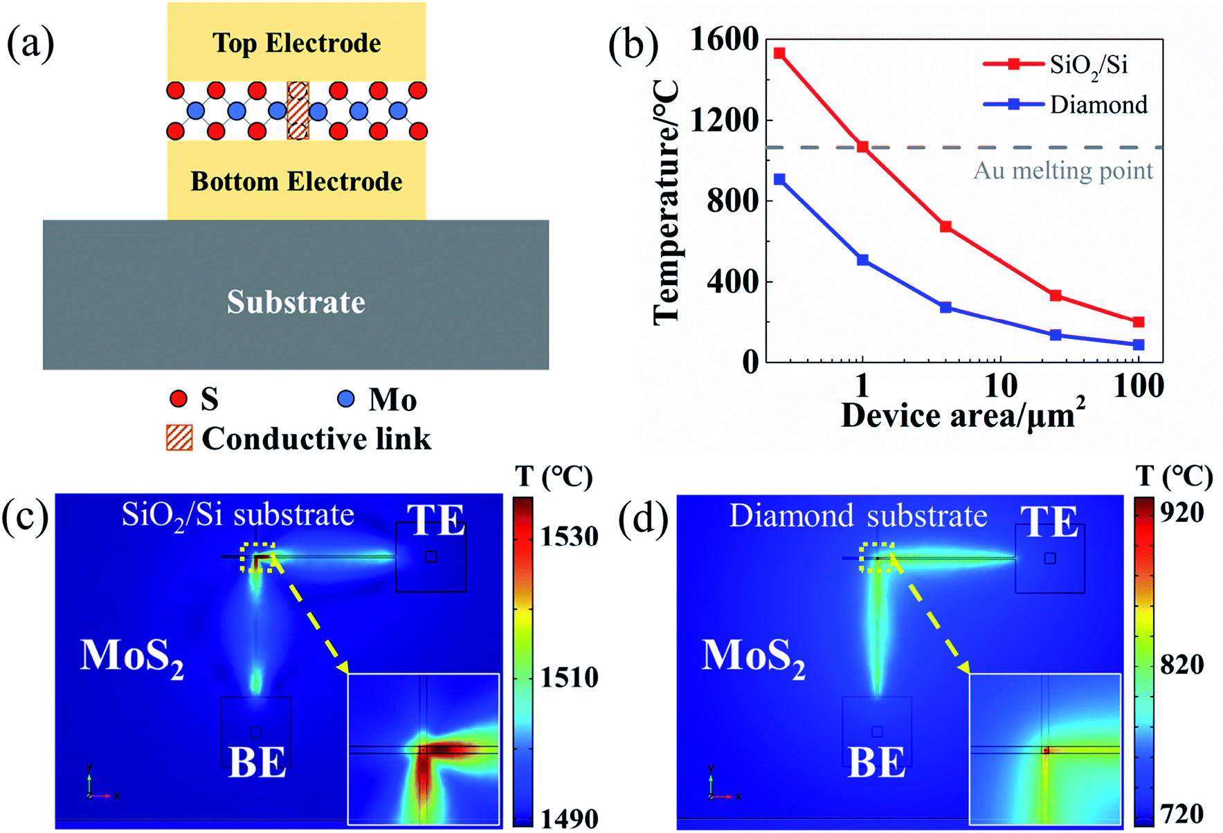 | ||
| Fig. 5 Numerical simulation results of temperature distribution. (a) Schematic of cross-sectional MIM structure of MoS2 NVRS device at LRS on SiO2/Si or diamond substrate. (b) Calculated peak temperature with different device areas on SiO2/Si and diamond substrate. The temperature distribution of MoS2 crossbar device on (c) SiO2/Si and (d) diamond substrate. The temperature induced by Joule heating effect reduces significantly for device on diamond substrate due to its high thermal conductivity. | ||
4 Conclusion
In summary, we performed CVS and CCS tests on MoS2-based 2D memory devices. The resistance evolution results disclose an additional resistance state which can be achieved by low CVS treatment on the devices at HRS. A modified conductive-bridge-like model based on metal atom/ion migration is proposed to explain the stress effects. Our results provide additional insights into resistance states transition, device reliability and applications of 2D atomristors.Conflicts of interest
There are no conflicts to declare.Acknowledgements
This work was supported in part by the National Science Foundation (NSF) grant #1809017. The authors acknowledge use of Texas Nanofabrication Facilities supported by the NSF NNCI award #1542159. D. A. acknowledges the Presidential Early Career Award for Scientists and Engineers (PECASE) through the Army Research Office (W911NF-16-1-0277).References
- C. Hao, F. Wen, J. Xiang, S. Yuan, B. Yang, L. Li, W. Wang, Z. Zeng, L. Wang, Z. Liu and Y. Tian, Adv. Funct. Mater., 2016, 26, 2016–2024 CrossRef CAS.
- C. Pan, Y. Ji, N. Xiao, F. Hui, K. Tang, Y. Guo, X. Xie, F. M. Puglisi, L. Larcher, E. Miranda, L. Jiang, Y. Shi, I. Valov, P. C. McIntyre, R. Waser and M. Lanza, Adv. Funct. Mater., 2017, 27, 1604811 CrossRef.
- S. K. Pradhan, B. Xiao, S. Mishra, A. Killam and A. K. Pradhan, Sci. Rep., 2016, 6, 26763 CrossRef CAS.
- X. Wu, R. Ge, P. A. Chen, H. Chou, Z. Zhang, Y. Zhang, S. Banerjee, M. H. Chiang, J. C. Lee and D. Akinwande, Adv. Mater., 2019, 31, e1806790 CrossRef.
- V. K. Sangwan, D. Jariwala, I. S. Kim, K. S. Chen, T. J. Marks, L. J. Lauhon and M. C. Hersam, Nat. Nanotechnol., 2015, 10, 403–406 CrossRef CAS.
- R. Xu, H. Jang, M. H. Lee, D. Amanov, Y. Cho, H. Kim, S. Park, H. J. Shin and D. Ham, Nano Lett., 2019, 19, 2411–2417 CrossRef CAS.
- H. S. P. Wong, H. Lee, S. Yu, Y. Chen, Y. Wu, P. Chen, B. Lee, F. T. Chen and M. Tsai, Proc. IEEE, 2012, 100, 20 Search PubMed.
- F. Zhou, Y.-F. Cang, K. Byun, B. Fowler and J. C. Lee, Appl. Phys. Lett., 2014, 105, 133501 CrossRef.
- Y. C. Chen, S. T. Hu, C. Y. Lin, B. Fowler, H. C. Huang, C. C. Lin, S. Kim, Y. F. Chang and J. C. Lee, Nanoscale, 2018, 10, 15608–15614 RSC.
- B. Sun, G. D. Zhou, T. Guo, Y. N. Zhou and Y. M. A. Wu, Nano Energy, 2020, 75, 20 Search PubMed.
- B. L. Guo, B. Sun, W. T. Hou, Y. Z. Chen, S. H. Zhu, S. S. Mao, L. Zheng, M. Lei, B. Li and G. Q. Fu, RSC Adv., 2019, 9, 12436–12440 RSC.
- D. Akinwande, C. Huyghebaert, C. H. Wang, M. I. Serna, S. Goossens, L. J. Li, H. P. Wong and F. H. L. Koppens, Nature, 2019, 573, 507–518 CrossRef CAS.
- D. Akinwande, N. Petrone and J. Hone, Nat. Commun., 2014, 5, 5678 CrossRef CAS.
- F. Hui, E. Grustan-Gutierrez, S. Long, Q. Liu, A. K. Ott, A. C. Ferrari and M. Lanza, Adv. Electron. Mater., 2017, 3, 1600195 CrossRef.
- W. D. Lu, 2019 Device Research Conference (DRC), Ann Arbor, MI, USA, 2019 Search PubMed.
- R. Ge, X. Wu, M. Kim, J. Shi, S. Sonde, L. Tao, Y. Zhang, J. C. Lee and D. Akinwande, Nano Lett., 2018, 18, 434–441 CrossRef CAS.
- R. Ge, X. Wu, M. Kim, P. Chen, J. Shi, J. Choi, X. Li, Y. Zhang, M. Chiang, J. C. Lee and D. Akinwande, 2018 IEEE International Electron Devices Meeting (IEDM), San Francisco, CA, USA, 2018 Search PubMed.
- M. Kim, R. Ge, X. Wu, X. Lan, J. Tice, J. C. Lee and D. Akinwande, Nat. Commun., 2018, 9, 2524 CrossRef.
- M. Kim, E. Pallecchi, R. Ge, X. Wu, V. Avramovic, E. Okada, J. C. Lee, H. Happy and D. Akinwande, 2019 IEEE International Electron Devices Meeting (IEDM), San Francisco, CA, USA, 2019 Search PubMed.
- Y. S. Chen, H. Y. Lee, P. S. Chen, P. Y. Gu, C. W. Chen, W. P. Lin, W. H. Liu, Y. Y. Hsu, S. S. Sheu, P. C. Chiang, W. S. Chen, F. T. Chen, C. H. Lien and M. Tsai, 2009 IEEE International Electron Devices Meeting (IEDM), Baltimore, MD, USA, 2009 Search PubMed.
- H. Xie, Q. Liu, Y. Li, H. Lv, M. Wang, K. Zhang, S. Long, S. Liu and M. Liu, Semicond. Sci. Technol., 2012, 27, 105007 CrossRef.
- G. Wang, S. Long, M. Zhang, Y. Li, X. Xu, H. Liu, M. Wang, P. Sun, H. Sun, Q. Liu, H. Lü, B. Yang and M. Liu, Sci. China: Technol. Sci., 2014, 57, 2295–2304 CrossRef.
- A. Prakash, S. Maikap, S. Z. Rahaman, S. Majumdar, S. Manna and S. K. Ray, Nanoscale Res. Lett., 2013, 8, 220 CrossRef.
- P. Lorenzi, R. Rao and F. Irrera, Microelectron. Reliab., 2015, 55, 1446–1449 CrossRef CAS.
- H. Li, Q. Zhang, C. Yap, B. Tay, T. Edwin, A. Olivier and D. Baillargeat, Adv. Funct. Mater., 2012, 22, 1385–1390 CrossRef CAS.
- D. Lee, D. J. Seong, H. J. Choi, I. Jo, R. Dong, W. Xiang, S. Oh, M. Pyun, S. O. Seo, S. Heo, M. Jo, D. K. Hwang, H. K. Park, M. Chang, M. Hasan, H. Hwang and IEEE, 2006 International Electron Devices Meeting, 2006, vol. 1–2, p. 551-+ Search PubMed.
- Y. J. Chen, H. L. Chen, T. F. Young, T. C. Chang, T. M. Tsai, K. C. Chang, R. Zhang, K. H. Chen, J. C. Lou, T. J. Chu, J. H. Chen, D. H. Bao and S. M. Sze, Nanoscale Res. Lett., 2014, 9, 5 CrossRef.
- F. Zahoor, T. Z. A. Zulkifli and F. A. Khanday, Nanoscale Res. Lett., 2020, 15, 26 CrossRef.
- D. Le, T. B. Rawal and T. S. Rahman, J. Phys. Chem. C, 2014, 118, 5346–5351 CrossRef CAS.
- D. Liu, Y. Guo, L. Fang and J. Robertson, Appl. Phys. Lett., 2013, 103, 183113 CrossRef.
- S. M. Hus, R. Ge, P.-A. Chen, M.-H. Chiang, G. E. Donnelly, W. Ko, F. Huang, L. Liang, A.-P. Li and D. Akinwande, Nat. Nanotechnol., 2020 DOI:10.1038/s41565-020-00789-w.
- Y. Liu, J. Guo, E. B. Zhu, L. Liao, S. J. Lee, M. N. Ding, I. Shakir, V. Gambin, Y. Huang and X. F. Duan, Nature, 2018, 557, 696–700 CrossRef CAS.
- L. G. Kong, X. D. Zhang, Q. Y. Tao, M. L. Zhang, W. Q. Dang, Z. W. Li, L. P. Feng, L. Liao, X. F. Duan and Y. Liu, Nat. Commun., 2020, 11, 7 CrossRef.
- G. D. Zhou, J. G. Wu, L. D. Wang, B. Sun, Z. J. Ren, C. Y. Xu, Y. Q. Yao, L. P. Liao, G. Wang, S. H. Zheng, P. Mazumder, S. K. Duan and Q. L. Song, Nanoscale, 2019, 11, 17222–17229 RSC.
- G. D. Zhou, X. D. Yang, L. H. Xiao, B. Sun and A. K. Zhou, Appl. Phys. Lett., 2019, 114, 5 Search PubMed.
- L. Zhao, Z. Jiang, H. Y. Chen, J. Sohn, K. Okabe, B. Magyari-Kope, H. S. P. Wong, Y. Nishi and IEEE, 2014 IEEE International Electron Devices Meeting (IEDM), 2014, p. 4 Search PubMed.
- M. Wang, S. H. Cai, C. Pan, C. Y. Wang, X. J. Lian, Y. Zhuo, K. Xu, T. J. Cao, X. Q. Pan, B. G. Wang, S. J. Liang, J. J. Yang, P. Wang and F. Miao, Nat. Electron., 2018, 1, 130–136 CrossRef CAS.
Footnote |
| † Electronic supplementary information (ESI) available. See DOI: 10.1039/d0ra05209d |
| This journal is © The Royal Society of Chemistry 2020 |