
 Open Access Article
 This Open Access Article is licensed under a Creative Commons Attribution-Non Commercial 3.0 Unported Licence
Effect of morphology and impact of the electrode/electrolyte interface on the PEC response of Fe2O3 based systems – comparison of two preparation techniques†
Kumari Ashaa,
Vibha Rani Satsangi b,
Rohit Shrivastava,
Rama Kantc and
Sahab Dass*a
b,
Rohit Shrivastava,
Rama Kantc and
Sahab Dass*a
aDepartment of Chemistry, Faculty of Science, Dayalbagh Educational Institute, Dayalbagh, Agra, 282005, India. E-mail: drsahabdas@gmail.com
bDepartment of Physics & Computer Science, Faculty of Science, Dayalbagh Educational Institute, Dayalbagh, Agra, 282005, India
cDepartment of Chemistry, University of Delhi, Delhi, 110007, India
First published on 19th November 2020
Abstract
The present study is a comparative account of Fe2O3 based photoelectrodes prepared by two different techniques, namely spray pyrolysis and electrochemical deposition, followed by photoelectrochemical analysis at pH 13 (highly alkaline) and pH 8 (near neutral) in 0.1 M NaOH solution for solar hydrogen generation. The study also investigates the influence of morphology at the semiconductor electrode/electrolyte interface along with quantitative determination of the morphological parameters of the rough electrode surface affecting the photoelectrochemical response using power spectral density analysis. Studies revealed that the Fe2O3 sample (E_100cy) prepared with 100 cycles of electrochemical deposition showed the highest photocurrent density of 2.37 mA cm−2 and 1.18 mA cm−2 at 1 V vs. SCE at pH 13 and 8 respectively. Power spectral density analysis exhibited that E_100cy possesses smallest surface features contributing to the PEC response with a lower cut off length scale of 17.23, upper cut off length scale of 150.45, maximum fractal dimension of 2.62 and maximum average rms roughness of 17.52 nm, offering the maximum surface area for charge transfer reactions at the electrode/electrolyte interface. The sample E_100cy exhibited the highest ABPE of 1.29% and IPCE of 37.5%.
1. Introduction
Solar driven water splitting also known as photoelectrochemical water splitting is one of the most promising techniques to produce hydrogen efficiently.1 The demand of energy for the enormously growing population can be met by sustainable exploitation of renewable energy resources. From this perspective, hydrogen has attracted the attention of researchers worldwide due to its significantly high energy density of 120 MJ kg−1.2 One of the major advantages of using this technique is that it produces hydrogen in the cleanest way possible and hence it is environmental friendly and an efficient approach.3,4 Ever since the electrochemical photolysis experiment carried out on TiO2 by Fujishima and Honda in 1972, researchers across the globe have been investigating PEC water splitting intensively.5 In the past four decades, various semiconductor materials other than TiO2 have been studied for their use as photoelectrode in PEC splitting of water.Hematite (α-Fe2O3) is one of the most extensively used and promising semiconductor material which has gained significant attention as photoanode owing to its attractive properties viz. absorption in visible region which is approximately 40% of the solar spectrum, band gap of ∼2.2 eV, stability in aqueous solutions, abundance and cost effectiveness.1,6 The major challenge associated with hematite in PEC system is high rate of electron–hole pair recombination, poor diffusion length of minority charge carriers (2–4 nm), low depth of solar light penetration (α−1 = 118 nm at λ = 550 nm) and slow kinetics of oxygen evolution reaction.7–10 All these factors lead to reduced solar to chemical conversion efficiency and poor PEC performance of α-Fe2O3.
Many modifications have been adopted to tune the morphological, optical and electronic properties of α-Fe2O3 in order to make it a suitable and ideal candidate for efficient solar water splitting. Enormous effort has been put in since 1972 in order to make PEC technology commercially viable by employing strategies like nano-structuring,7,11 doping,1,12 formations of heterojunction,13–16 low energy and swift heavy ion irradiation,17,18 deposition of catalyst19 etc.
Fabrication of hematite thin films has been done in the past by variety of procedures viz. hydrothermal method,20–23 chemical vapor deposition,7,8 sputtering,24 electrochemical deposition,9,25 spray pyrolysis,13,26 etc. and it was seen that the response of the material definitely depends on its method of preparation. Besides the method of preparation, reports are available that photoresponse does get affected due to particles of different shape and size, roughness, porosity and overall thickness of the deposition. In other words, the morphology of nanoparticles varies with the method of preparation which may in turn alter the optical and electronic properties and overall performance of PEC system.27,28 Morphological related study on Fe2O3 has been conducted by Sun et al. in which α-Fe2O3 films were fabricated using hydrothermal method with two different sets of precursors leading to formation of α-Fe2O3 with different morphologies resulting in increased PEC response.29 Electrochemical parameters like current,30–33 impedance,27 absorbance34 and charge transients30,35 have been studied in detail theoretically to establish correlation vis a vis morphology of the electrode.
Besides morphology there are other factors such as electrolyte, pH of electrolyte, annealing temperature etc. that have also been studied and are linked to be equally responsible for the photoelectrochemical performance and stability of photoelectrodes. Studies conducted on TiO2, ZnO, BiVO4, Fe2O3, etc. report significant alteration in the photocurrent due to variation in the pH of electrolyte.8,14,36–38 Studies have also been conducted on the investigation of PEC performance of photoelectrodes in neutral or near neutral pH.8,14,19,39 Comparative studies on Ti doped Fe2O3 with Co–Ac catalyst have been performed at pH 8 and 12.5 by Banerjee et al.19 However, poor photoelectrochemical performance and stability in neutral pH electrolyte in case of low band gap materials such as Fe2O3 based systems is a major concern. In order to make PEC technique a commercially viable and common practice for solar hydrogen generation we require photoelectrode systems which are ubiquitous in nature, cost effective to synthesize, have low band gap so that they can absorb maximum portion of solar spectrum, eco-friendly and most importantly, can work under neutral to near neutral pH electrolyte.
The present communication attempts fabrication of pristine hematite films by economic and facile methods of spray pyrolysis and electrochemical deposition for their application in highly alkaline to near neutral pH electrolyte. Photoelectrochemical performances of electrodes prepared by both the techniques were studied separately in 0.1 M NaOH solution at highly alkaline pH 13. The optimized electrodes with the best PEC response were chosen for further comparative studies at a near neutral pH 8 in 0.1 M NaOH solution and were characterized using X-ray diffraction spectroscopy (XRD), Atomic force microscopy (AFM), Field-emission scanning electron microscopy (FE-SEM), Power Spectral Density (PSD) analysis etc. Power Spectral Density (PSD) analysis which is an important and powerful tool has been used for quantitative examination of the morphology of rough surface topography of hematite electrodes apparently for the first time. A power spectrum (PS) of the rough surface obtained from PSD analysis provides quantitative measure of various surface roughness parameters like lower (l) cut-off length scale, upper (L) cut-off length scale and fractal dimension (DH). The surface profile of a rough electrode is converted into its corresponding spatial wavelengths over the sampling area.33 The smallest surface feature taking part in electrochemical reaction is the lower (l) cut-off length scale while the largest surface feature is the upper (L) cut-off length scale. The fractal dimension (DH) describes the roughness scale and is indicative of the distribution of fractal surfaces in space.40,41 Morphological parameters obtained for electrodeposited and spray deposited hematite electrodes were interpreted and correlated with electrochemical and photoelectrochemical results to draw a characteristic relationship between the morphology and PEC performance of hematite electrodes.
2. Experimental
2.1. Sample preparation
| Sr. no. | Description of prepared thin films | Sample acronym | Average film thickness | Average crystallite size (nm) |
|---|---|---|---|---|
| 1 | Fe2O3 film electrodeposited with 50 cycles | E_50cy | 550 nm | 75 |
| 2 | Fe2O3 film electrodeposited with 100 cycles | E_100cy | 1 μm | 80 |
| 3 | Fe2O3 film electrodeposited with 150 cycles | E_150cy | 1.5 μm | 90 |
| 4 | Spray pyrolytically deposited Fe2O3 film for 20 s | S_20s | 250 nm | 25 |
| 5 | Spray pyrolytically deposited Fe2O3 film for 30 s | S_30s | 380 nm | 33 |
| 6 | Spray pyrolytically deposited Fe2O3 film for 40 s | S_40s | 520 nm | 45 |
| 7 | Spray pyrolytically deposited Fe2O3 film for 50 s | S_50s | 600 nm | 40 |
2.2. Characterizations
The X-ray diffraction (XRD) patterns of spray pyrolytically and electrodeposited thin films of Fe2O3 were recorded with X-ray diffractometer (Bruker AXS, D8 Advance) using Cu Kα radiation (λ = 1.5418 Å). The glancing angle (2θ) was varied from 20° to 60° to record the XRD pattern. Debye–Scherrer equation was employed to determine the crystallite phase and crystallite size. Information about the morphology and topography of thin films prepared by both the methods were obtained by Field-Emission Scanning Electron Microscopy (FE-SEM, Tescan Mira II LMH) and Atomic Force Microscopy (AFM, Nanoscope IIIa Scanning Microscope Controller, Digital Instruments) respectively. Optical absorption spectra for all the Fe2O3 samples were measured with the help of UV-visible spectrophotometer (Shimadzu, UV-2450). The obtained absorption spectrums were further studied to determine band gap of all the samples. Thickness of all the prepared Fe2O3 thin films was determined by means of surface profilometer (Bruker DektakXT).2.3. Power spectral density analysis
Power spectrum which reveals information about all the roughness parameters was obtained from AFM images of spray pyrolytically and electrodeposited Fe2O3 samples. To serve this purpose, AFM images of Fe2O3 thin films prepared using spray pyrolysis and electrodeposition methods were recorded at varying resolutions. These AFM images were analyzed by Nanoscope analysis software associated with the scanning probe instrument to obtain the power spectrum. The power spectrum so obtained was further interpreted to calculate the morphological parameters such as lower cut off length scale (l), upper cut off length scale (L) and the fractal dimension (DH).2.4. Electrochemical and photoelectrochemical studies
All the prepared Fe2O3 thin films were subjected to electrochemical and photoelectrochemical measurements inside a three electrode assembly cell filled with 0.1 M NaOH (at pH 13 and 8) electrolyte kept in a quartz compartment at room temperature. 0.1 M NaOH solution of pH 8 was prepared by neutralizing 0.1 M NaOH solution of pH 13 with 1 M H3PO4 which reduces the pH without affecting the molarity. Thin films of Fe2O3 were employed as the working electrode, platinum mesh as the counter electrode and saturated calomel electrode (SCE) as the reference electrode. The whole system was connected to an electrochemical work station (Zahner Zehnnium-PP211, Germany). Fe2O3 electrodes with an area of 1 cm2 were exposed to solar radiations using a 150 W xenon arc lamp (Newport, RI, USA) with intensity of 1 sun illumination (100 mW cm−2). Photocurrent density analysis was conducted with an applied bias being varied from −1.0 V to 1.0 V vs. SCE at the scan rate of 10 mV s−1. Transient open circuit potential studies were conducted for all the electrodes at regular interval of 20 s for duration of 120 seconds. Mott–Schottky measurements were also carried out to measure the capacitance (C) of the electrical double layer for all the Fe2O3 electrodes in dark condition. The applied bias was varied from −1 V to 1 V at 5 mV amplitude with an operating AC signal frequency of 1 kHz. The Mott–Schottky curve follows the following equation:46
 | (1) |
Electrochemical impedance spectroscopy (EIS) is an important technique to study the charge transfer kinetics at the semiconductor electrode/electrolyte interface. For this, a sinusoidal AC frequency at 5 mV amplitude was varied from 100 mHz to 10 kHz in sweep mode. Nyquist and Bode plot were obtained under dark and illumination for all the samples.
2.5. Efficiency measurements
Applied bias photon-to-current efficiency (ABPE) is calculated by using the following equation:13
 | (2) |
Incident photon-to-current efficiency (IPCE) was recorded using Zahner, PP211 (CIMPS-pcs, Germany) electrochemical workstation within a three electrode cell. The measurements were carried out in the illumination range of 350–800 nm.
Chronoamperometric measurements were performed to check for the stability of the prepared electrodes under illumination for duration of 1 hour in near neutral pH i.e. 8.
3. Results and discussion
3.1. Crystallite size and phase analysis
The X-ray diffraction patterns of the thin film samples of Fe2O3 prepared by spray pyrolysis and electrodeposition are shown in Fig. 1(A and B) respectively. The prominent peaks in Fig. 1(A) at 24.16°, 33.18°, 35.65°, 40.88°, 49.49°, 54.10° belong to respective (012), (104), (110), (113), (024) and (116) planes for rhombohedral system of hematite phase of Fe2O3 and are confirmed by the JCPDS card no. 01-073-2234. The remaining peaks correspond to the underlying substrate ITO. In Fig. 1(B), the peaks at glancing angle (2θ) of 24.16°, 33.19°, 35.65°, 40.89°, 49.50° and 54.12° correspond to (012), (104), (110), (113), (024) and (116) planes respectively and corresponds to the JCPDS card no. 01-085-0599. All these peaks confirm the hematite phase with rhombohedral system of Fe2O3. The other peaks in the XRD pattern are of the FTO substrate. The average crystallite size of all the samples were calculated using Debye–Scherrer equation and are reported in Table 1.47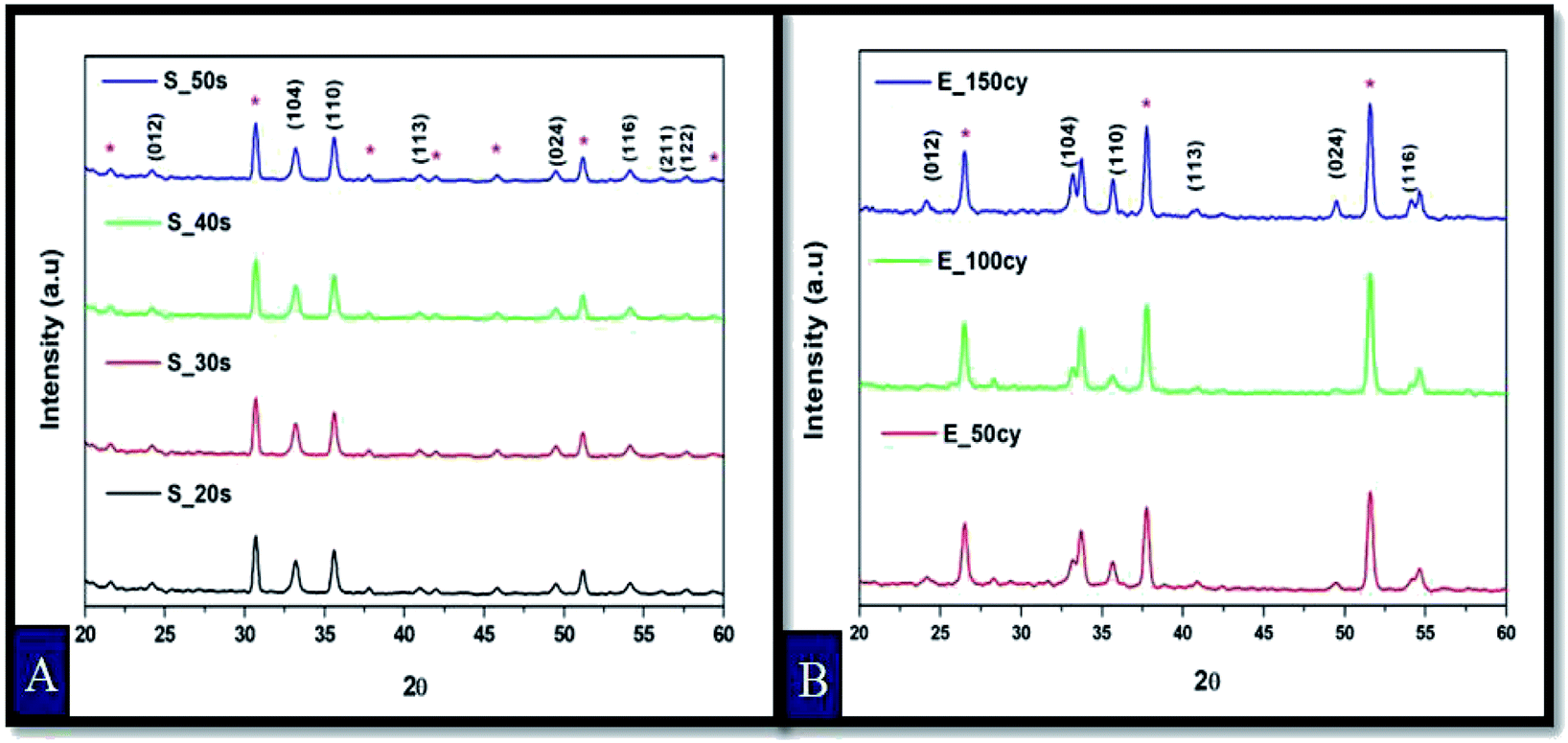 | ||
| Fig. 1 XRD patterns of Fe2O3 thin films prepared by (A) spray pyrolysis and (B) electrodeposition. | ||
3.2. Photoelectrochemical analysis
Steady state photocurrent density plots as a function of applied potential (V vs. SCE) for all the samples are shown in Fig. 2. Studies conducted at pH 13 i.e. under high alkaline conditions, reveals that all the Fe2O3 electrodes synthesized by spray pyrolysis technique exhibit lower photocurrent as compared to the Fe2O3 electrodes prepared by electrochemical deposition. In case of the electrodes prepared by spray pyrolysis, the sample with spray deposition time of 40 s i.e. sample S_40s exhibits the maximum photocurrent density of 0.43 mA cm−2 at 1 V vs. SCE (Fig. 2(A)) while under similar pH conditions, the electrodeposited Fe2O3 sample with 100 cycles of deposition exhibited photocurrent density of 2.37 mA cm−2 at 1 V vs. SCE with a decrease in the onset potential by ∼200 mV (Fig. 2(B)). The photocurrent density values for E_100cy showed approximately 5.5 fold enhancement as compared to S_40s. Photoelectrochemical response of hematite largely depends on the quantity of the photoactive material deposited on the substrate which is directly related to the thickness of the film. For this reason, the photocurrent density increases with the increase in the spray time of deposition in case of spray deposition and increase in the number of cycles for electrochemical deposition. After reaching an optimal concentration of Fe2O3 material, a decrease in the photocurrent density values is observed in both the case of deposition of Fe2O3.19,48 Hence, photocurrent density values decrease for S_50s and E_150cy. The excess deposition on the substrate reduces the diffusion length of holes by hampering their transfer to the semiconductor/electrolyte interface.19,49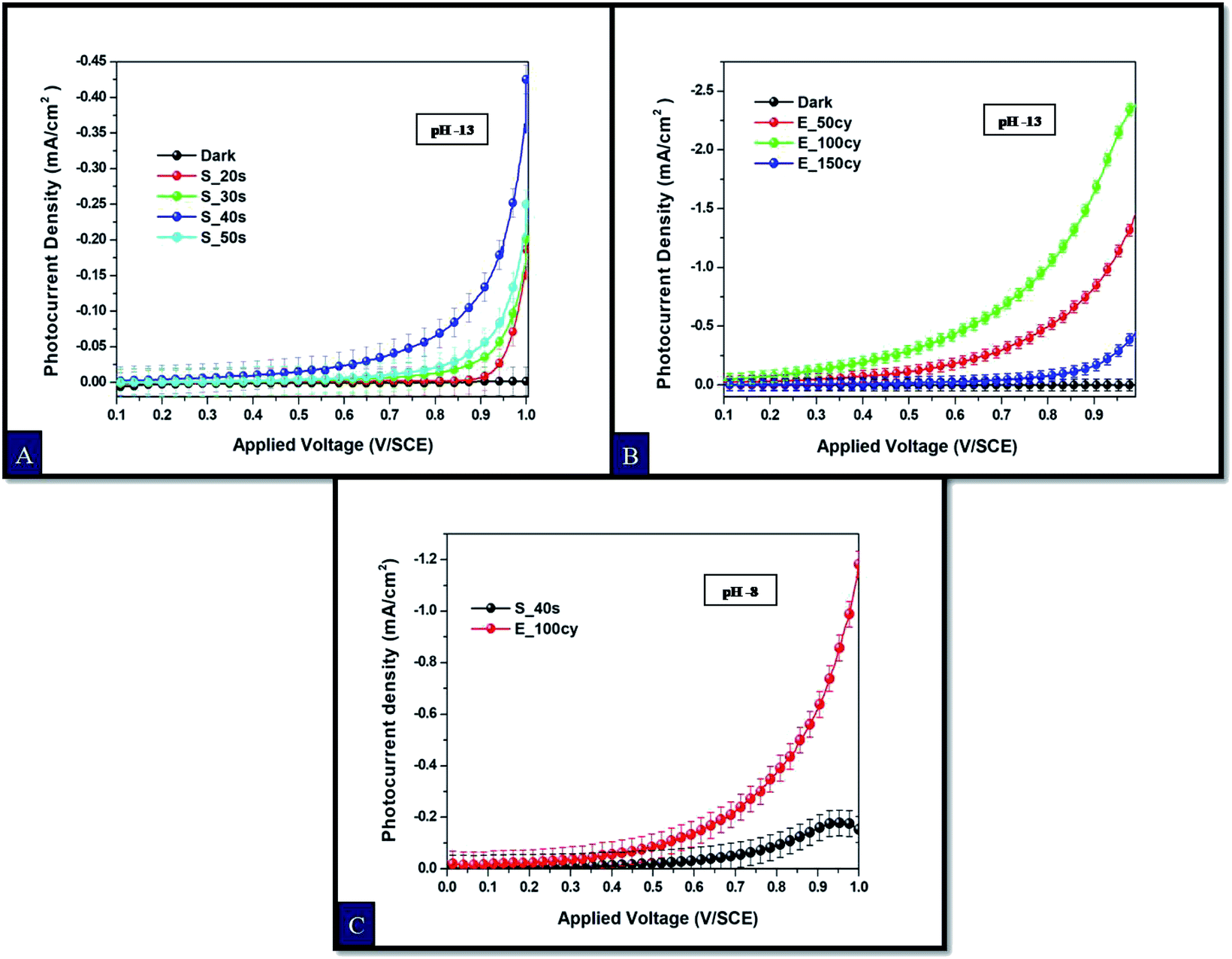 | ||
| Fig. 2 Photocurrent density curves of Fe2O3 electrodes at pH 13 in 0.1 M NaOH solution prepared by (A) spray pyrolysis, (B) electrodeposition and (C) comparative photocurrent density curves at pH 8. | ||
From this study, spray and electrochemically deposited Fe2O3 samples exhibiting the highest photoresponse at pH 13 i.e. samples E_100cy and S_40s were chosen to be studied for further analysis at pH 8. The comparative photocurrent density analysis (Fig. 2(C)) for the samples E_100cy and S_40s at pH 8 reveals that photocurrent density values decreased significantly at pH 8. However, the electrodeposited Fe2O3 electrode remains the best sample out of the two and shows highest photocurrent density of 1.18 mA cm−2 at 1 V vs. SCE with ∼8 fold increment in comparison to the spray deposited sample with photocurrent density of 0.15 mA cm−2 at 1 V vs. SCE. Comparison of photoelectrochemical performances of the samples S_40s and E_100cy at the studied pH i.e. 13 and 8 shows that the photocurrent density values of S_40s sample decreased considerably by ∼3 fold while for E_100cy it reduced by ∼2 fold.8 The onset potential for the sample S_40s increased from 0.40 V (at pH 13) to 0.52 V (at pH 8) with a shift of 220 mV whereas, in case of E_100cy, the onset potential remained at 0.20 V. Lower values of onset potential mark faster transfer of holes towards the semiconductor/electrolyte interface which in turn hinder electron hole pair recombination in the bulk of semiconductor.49
3.3. Surface morphology analysis
Fe2O3 samples exhibiting the highest photoresponse i.e. S_40s and E_100cy were examined by Field-emission scanning electron microscopy for the analysis of morphological factors contributing to higher photoelectrochemical response. Scanning electron micrographs of S_40s and E_100cy samples are shown in Fig. 3. The SEM image of spray pyrolytically deposited sample S_40s (Fig. 3(A)) shows compact and uniform packing of the spindle shaped or rhombohedral grains. The morphology of particles reveals mesoporous deposition throughout the film surface. The grain size varies from 30–60 nm and is in agreement with the crystallite size measured from XRD analysis.50 FE-SEM images of all the spray deposited samples are provided in Fig. S1.† It is clear from the Fig. S1† that the number of grains and the porosity increases with the increase in deposition time from 20 s to 40 s. The thin film sample S_40s seems to be the sample with clearly defined grains and least agglomeration. The sample has highly mesoporous network of grains. As the deposition time is further increased to 50 s, grain size decreases and agglomeration of grains is seen. The thickness of film increases with the increase in the deposition time. Thinner films like S_20s and S_30s do not possess sufficient number of grains to absorb maximum portion of solar spectrum.24 Fig. 3(B) shows FE-SEM image of E_100cy Fe2O3 sample. The micrograph reveals highly porous network of particles consisting of hollow microspheres. The particles on the top appear highly rough which indicates that they consist of many loosely packed nanoparticles. Fig. S2† shows FE-SEM images of all the electrodeposited Fe2O3 samples. It can be seen that the number of particles and porosity of the film increases with the increase in the number of cycles of deposition.25 An optimum film thickness present in the sample S_40s (∼520 nm) and E_100cy (∼1 μm) allows maximum absorption of solar radiations and also prevents bulk recombination of charge carriers.19,51 As the film thickness increases further in case of S_50s (∼600 nm) and E_150cy (∼1.5 μm), charge carrier recombination becomes more prominent. In addition to this, increasing number of particles and grain boundaries lead to shorter diffusion length of holes to the semiconductor/electrolyte interface which in turn cause reduced PEC response.24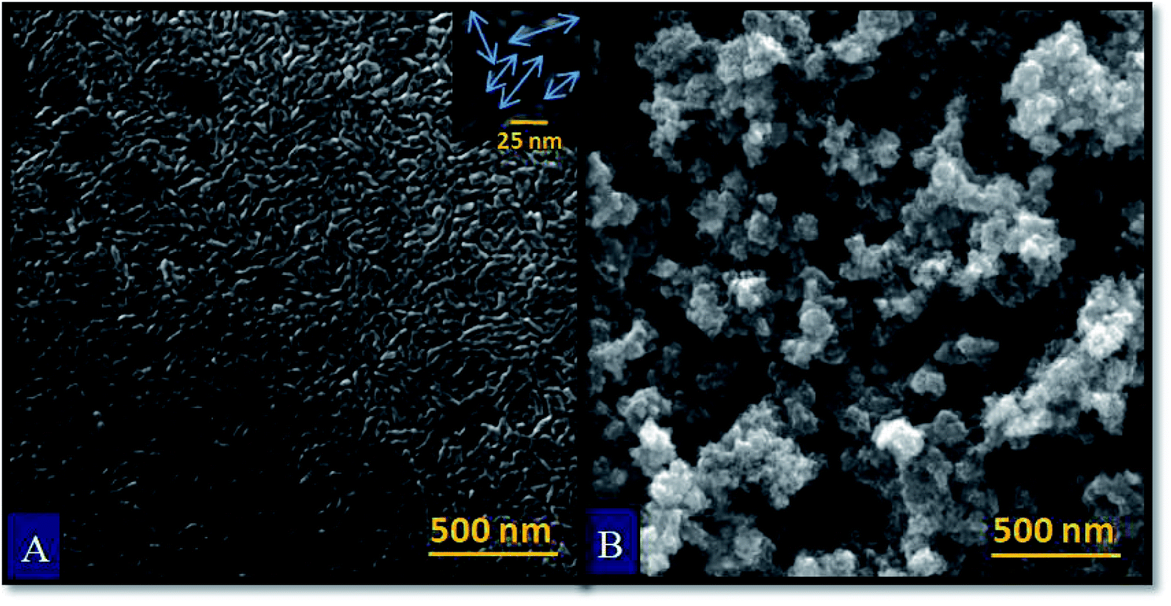 | ||
| Fig. 3 FE-SEM images of Fe2O3 thin films prepared by (A) spray pyrolysis and (B) electrodeposition. | ||
It is evident from the Fig. 3 that the morphology of particles deposited by spray and electrodeposition methods is totally different. The morphology of S_40s is compact with flat spindle and rhombohedral grains while particles in E_100cy are loosely arranged with highly porous framework. Higher photoresponse in E_100cy could be attributed to the thickness of film, high degree of porosity and rough nanoparticles.
3.4. Topographical analysis
Three dimensional atomic force micrographs of Fe2O3 samples S_40s and E_100cy are provided in the Fig. 4 for the analysis of surface topography. It is clearly observed from the micrographs that electrodeposited sample E_100cy possesses more surface roughness as compared to the spray pyrolytically deposited sample S_40s. Values of rms roughness for all the samples prepared are provided in Table 2. This increased roughness facilitates separation and transfer of electron and holes and thus prevents their recombination in the bulk of the semiconductor.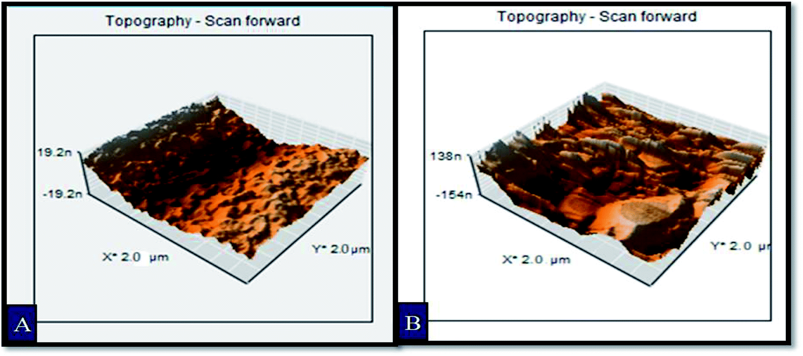 | ||
| Fig. 4 AFM images of Fe2O3 thin films prepared by (A) spray pyrolysis and (B) electrodeposition. | ||
| Sample description | Average PSD parameters | Rms roughness (nm) | ||
|---|---|---|---|---|
| DH | l (nm) | L (nm) | ||
| S_40s | 2.30 | 12.11 | 120.02 | 12.45 |
| E_100 cy | 2.62 | 17.23 | 150.45 | 17.52 |
3.5. Power spectral density (PSD) analysis
Power Spectral Density (PSD) measurements of all the prepared nanostructured Fe2O3 thin films were performed using AFM instrumentation. Power Spectral Density (PSD) analysis provides quantitative measurements of surface roughness parameters in the form of a curve of the amplitude of surface roughness with respect to spatial wavelengths. It thus helps in interpreting the surface features of a rough electrode and provides three dimensional information about the distribution of surface features. In PSD, A power-law spectrum is used to describe any rough surface. This spectrum consists of a wavenumbers scale as x-axis with a high and a low wavenumber cut-off. The intermediate region or the curved region in the power spectrum is the region between two flat regions of low and high wavenumber.52AFM images recorded at various resolutions were investigated by PSD analysis to obtain average values of surface roughness parameters such as lower cut off length scale (l), upper cut off length scale (L) and fractal dimension (DH). The method for calculation of surface roughness parameters has been explained elsewhere.41 The point considered for calculation of lower cut off length scale and upper cut off length scale are indicated in Fig. 5 by smaller arrows at high wavenumber region and longer arrows at low wavenumber region of power spectrum respectively. It can be observed that the lower and higher cut off length values of the sample prepared by electrochemical deposition E_100cy are at the lower wavenumbers in comparison to the sample prepared by spray pyrolysis S_40s. The corresponding values of all the roughness parameters for S_40s and E_100cy are reported in Table 2. However, the fractal dimension calculated from the slope of the curve which represents the distribution of fractal surfaces in space is higher for E_100cy. An increase in the DH is indicative of amplification in the number of clefts or folds on the surface of electrode which makes the film uneven and rougher. This clearly indicates that the sample E_100cy has highly distributed three dimensional arrangements of rough surface features as compared to the sample S_40s.
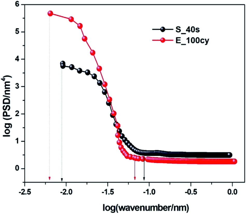 | ||
| Fig. 5 Power spectrum of Fe2O3 thin films prepared by spray pyrolysis and electrodeposition. | ||
3.6. EIS and PEIS measurements
Electrochemical impedance analysis was conducted to obtain Nyquist and Bode plot (Fig. 6). An in-depth understanding of the charge transfer kinetics at the electrode/electrolyte interface can be acquired by this powerful technique. Fig. 6(A and B) shows Nyquist plots obtained for dark and illumination studies of Fe2O3 samples. Inset in Fig. 6(B) represents the equivalent Randles circuit for the systems studied. Randles circuit parameters for fitting EIS data are shown in Table S1.† The sample E_100cy possesses the smallest semicircular curve in Fig. 6(A) which turns into shorter semicircles when exposed to solar radiations. This shortening of the semicircular curve indicates decline in the charge transfer resistance of the system.19 It is clear that sample prepared by electrochemical deposition possesses the least charge transfer resistance under both dark and illumination conditions.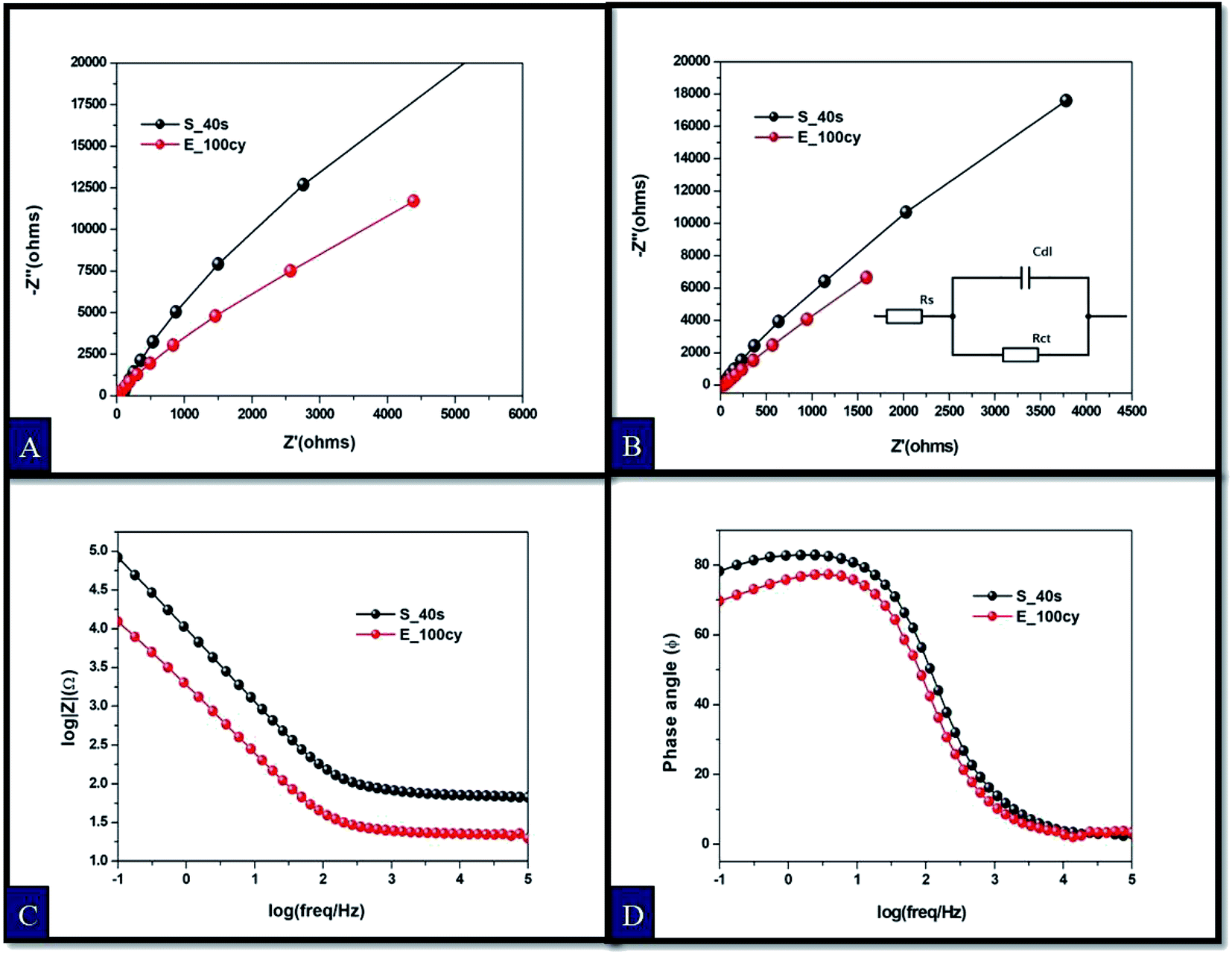 | ||
| Fig. 6 (A) Nyquist plot under dark, (B) Nyquist plot under illumination, (C) Bode absolute impedance plot and (D) Bode phase plot of Fe2O3 thin films prepared by spray pyrolysis and electrodeposition. | ||
Bode absolute impedance plot and Bode phase plot are shown in Fig. 6(C and D). Bode absolute impedance plot (Z) is a curve obtained from absolute values of impedance with respect to applied frequency while Bode phase plot is a plot of phase angle against frequency. The study was conducted in dark. It is observed that the magnitude of impedance decreased remarkably for E_100cy. It is reported that morphological factors of a surface, viz., roughness, porosity and fractal dimension greatly influence the impedance of an electrode.27 The phase plot shows lower value of phase angle for the sample E_100cy which represents increased heterogeneity of the electrode surface. All these results obtained are in agreement with the morphological parameters calculated from power spectrum. Sample E_100cy on account of having highest fractal dimension, least charge transfer resistance and impedance contributed more to photoelectrochemical response.
3.7. Optical absorption analysis
The optical absorbance spectra of thin film samples recorded using UV-vis spectrophotometer in 300–800 nm range is shown in Fig. S3(A).† An intense absorption edge is observed at 600 nm. Fe3+ 3d to 3d spin forbidden transition excitation is the reason for the absorption in the visible region.26 The sample prepared by electrodeposition (E_100cy) exhibits maximum absorption intensity as compared to the sample prepared by spray pyrolysis (S_40s) corresponding to the band gap of 2.0 eV as shown in Fig. S3(B).† The band gap of the sample S_40s is calculated to be 2.1 eV. The increased absorption in E_100cy could be attributed to increased thickness of film in case of the sample E_100cy (∼1 μm) which is significantly less in the sample S_40s (∼520 nm).513.8. Mott–Schottky analysis
Mott–Schottky was performed for both the spray and electrodeposited samples to acquire understanding about the kinetics of charge transfer at the semiconductor/electrolyte interface. The Mott–Schottky curve for both the samples S_40s and E_100cy is shown in Fig. S4.† The positive slope of the curve is obtained in both the samples which signify the n-type conductivity of Fe2O3 films. Flat band potential values were calculated from the intercept of curve at zero applied bias. It could be observed that the value of flat band potential for the sample S_40s is −0.20 V vs. SCE and for E_100cy it is −0.37 V vs. SCE. The more negative flat band potential value for the sample E_100cy indicates increased band bending which hampers the recombination of charge carriers in the bulk of semiconductor. This in turn promotes the separation of charge carriers at the semiconductor/electrolyte interface and thus aids in augmenting the PEC response.53 Donor density (ND) was calculated and is reported in Table 3 which is maximum in case of sample E_100cy. Higher donor density reduces the resistivity in the film and improves PEC response.| Sample description | Flat band potential VFB (V vs. SCE) | Donor density ND (cm−3) | Band gap (eV) | PCD at 1 V vs. SCE | % ABPE | % IPCE | Onset potential VOC (V vs. SCE) | ||
|---|---|---|---|---|---|---|---|---|---|
| At pH 8 | At pH 13 | At pH 8 | At pH 13 | ||||||
| S_40s | −0.20 | 9.60 × 10¹⁷ | 2.1 | 0.15 | 0.43 | 1.10 | 21.2 | 0.52 | 0.40 |
| E_100 cy | −0.37 | 7.84 × 10²⁰ | 2.0 | 1.18 | 2.37 | 1.29 | 37.5 | 0.20 | 0.20 |
3.9. Charge carrier recombination analysis and chronoamperometry studies
Charge carrier recombination kinetics was investigated from open circuit potential decay plots. For this purpose, transient open circuit potential curves were obtained for the sample S_40s and E_100cy with continuous light on and off cycles at the interval of 20 s as shown in Fig. 7A and B. This scan was conducted for two minutes. A cathodic shift in the open circuit potential was observed for both the samples which is in well agreement with the Mott–Schottky studies. This cathodic shift could be attributed to shift in the Fermi energy level.19 The open circuit potential value is higher for the sample E_100cy as compared to S_40s which indicated more charge recombination in case of S_40s.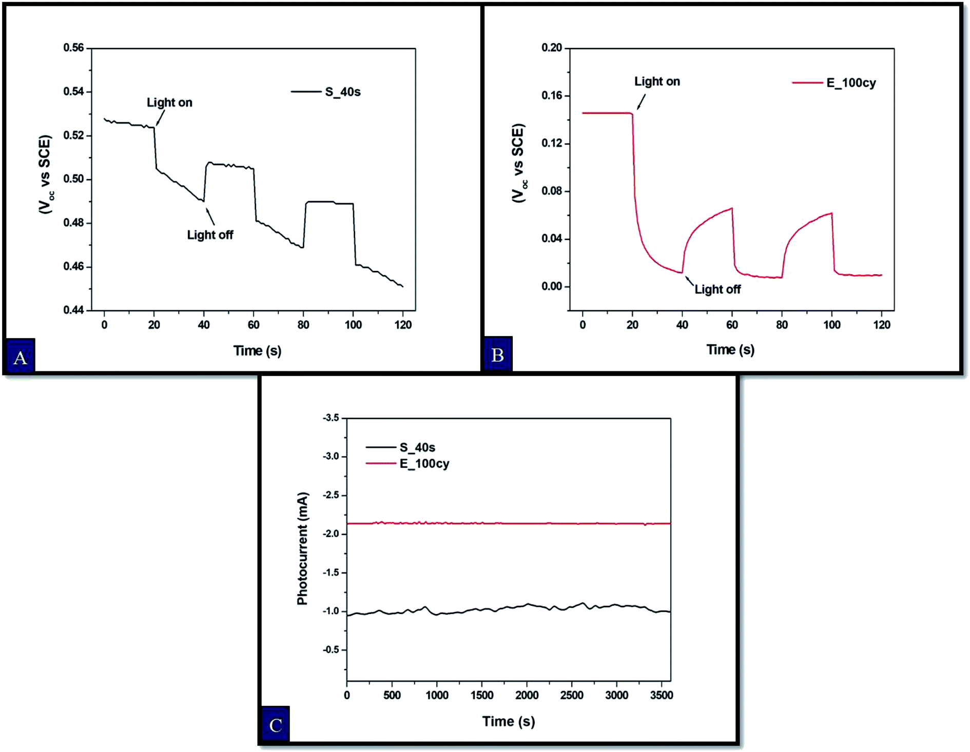 | ||
| Fig. 7 Transient open circuit potential curves for Fe2O3 thin films prepared by (A) spray pyrolysis, (B) electrodeposition and (C) chronoamperometry curves at pH 8 under constant illumination. | ||
Chronoamperometry measurements were also conducted to study the stability of the Fe2O3 samples S_40s and E_100cy under constant illumination at pH 8. The chronoamperometry curve is provided in Fig. 7(C), from which it is evident that the sample E_100cy exhibits higher photocurrent without much fluctuation for continuous duration of 1 hour. On the contrary, the curve for the sample S_40s seems noisy and gives lesser photocurrent under same conditions of electrolyte for 1 hour. Hence, the sample E_100cy is more stable as compared to S_40s.
3.10. Efficiency measurements
Applied bias photon-to-current efficiency (ABPE) was calculated for all the Fe2O3 samples using eqn (2). The sample E_100cy possesses the maximum efficiency of 1.29% while ABPE for S_40s is 1.10% at pH 8.The IPCE of all the samples as a function of wavelength is shown in Fig. 8. It is of greater significance as it represents generation of photocurrent as a result of absorption of photons by the semiconductor. It is clear that the absorption of photons by both the samples i.e. S_40s and E_100cy occurs in the visible region of solar spectrum. This is in well agreement with the data obtained from optical absorbance studies. A higher value of IPCE was obtained for the sample E_100cy which is 37.5% while S_40s exhibits IPCE of 21.2% at 1 V vs. SCE.
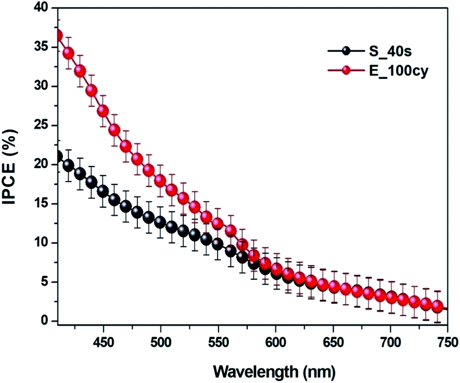 | ||
| Fig. 8 IPCE of Fe2O3 thin films prepared by spray pyrolysis and electrodeposition. | ||
4. Conclusions
Comparative study on the performance of α-Fe2O3 electrodes prepared by two different techniques viz. electrochemical deposition and spray pyrolysis in PEC system has been undertaken. α-Fe2O3 thin film samples prepared by both the techniques exhibiting the best response in 0.1 M NaOH solution at pH 13 were further studied at near neutral pH 8. Studies at pH 13 revealed that the Fe2O3 sample prepared by spray pyrolysis with 40 s deposition time (S_40s) and electrodeposited sample with 100 cycles of deposition (E_100cy) showed highest photocurrent density (PCD) of 0.43 mA cm−2 and 2.37 mA cm−2 respectively at 1 V vs. SCE. Further studies at pH 8 with the two best samples S_40s and E_100cy demonstrated that the sample E_100cy exhibited maximum PEC response with PCD of 1.18 mA cm−2 in comparison to S_40s (0.15 mA cm−2) at 1 V vs. SCE. Moreover, morphological parameters obtained from power spectral density analysis showed that E_100cy offered maximum surface area for charge transfer reactions at electrode/electrolyte interface owing to maximum fractal dimension of 2.62 and maximum average rms roughness of 17.52 nm. The sample E_100cy also exhibited highest ABPE of 1.29% and IPCE of 37.5%.Conflicts of interest
There are no conflicts to declare.Acknowledgements
The financial assistance to the work was provided by University Grants Commission (UGC), Government of India, Indo-US project vide no. ET/2155 and MNRE project file no. 103/241/2015-NT.References
- P. Kumar, P. Sharma, R. Shrivastav, S. Dass and V. R. Satsangi, Electrodeposited Zirconium-Doped α-Fe2O3 Thin Film for Photoelectrochemical Water Splitting, Int. J. Hydrogen Energy, 2011, 36(4), 2777–2784 CrossRef CAS.
- T. Shinagawa and K. Takanabe, Towards Versatile and Sustainable Hydrogen Production through Electrocatalytic Water Splitting: Electrolyte Engineering, ChemSusChem, 2017, 10(7), 1318–1336 CrossRef CAS.
- P. Tang and J. Arbiol, Engineering Surface States of Hematite Based Photoanodes for Boosting Photoelectrochemical Water Splitting, Nanoscale Horiz., 2019, 4, 1256–1276 RSC.
- Z. Li, W. Luo, M. Zhang, J. Feng and Z. Zou, Photoelectrochemical Cells for Solar Hydrogen Production: Current State of Promising Photoelectrodes, Methods to Improve Their Properties, and Outlook, Energy Environ. Sci., 2013, 6(2), 347–370 RSC.
- A. Fujishima and K. Honda, Electrochemical Photolysis of Water at a Semiconductor Electrode, Nature, 1972, 238, 37–38 CrossRef CAS.
- P. Sharma, J.-W. Jang and J. S. Sung, Key Strategies to Advance the Photoelectrochemical Water Splitting Performance of α-Fe2O3 Photoanode, ChemCatChem, 2018, 10, 1–24 CrossRef.
- M. Marelli, A. Naldoni, A. Minguzzi, M. Allieta, T. Virgili, G. Scavia, S. Recchia, R. Psaro and V. D. Santo, Hierarchical Hematite Nanoplatelets for Photoelectrochemical Water Splitting, ACS Appl. Mater. Interfaces, 2014, 6, 11997–12004 CrossRef CAS.
- R. Chong, B. Wang, C. Su, D. Li, L. Mao, Z. Chang and L. Zhang, Dual-Functional CoAl Layered Double Hydroxide Decorated α-Fe2O3 as an Efficient and Stable Photoanode for Photoelectrochemical Water Oxidation in Neutral Electrolyte, J. Mater. Chem. A, 2017, 5(18), 8583–8590 RSC.
- N. Kazemi, A. Maghsoudipour and T. Ebadzadeh, Electrochemical Preparation of Hematite Nanostructured Films for Solar Hydrogen Production, EPJ Web Conf., 2012, 33, 02007 CrossRef CAS.
- L. Wang, N. T. Nguyen, Y. Zhang, Y. Bi and P. Schmuki, Enhanced Solar Water Splitting by Swift Charge Separation in Au/FeOOH Sandwiched Single-Crystalline Fe2O3 Nanoflake Photoelectrodes, ChemSusChem, 2017, 10(13), 2720–2727 CrossRef CAS.
- A. A. Tahir, K. G. U. Wijayantha, S. Saremi-yarahmadi, M. Mazhar and V. Mckee, Nanostructured α-Fe2O3 Thin Films for Photoelectrochemical Hydrogen Generation, Int. J. Hydrogen Energy, 2009,(7), 3763–3772 CAS.
- A. Srivastav, A. Verma, A. Banerjee, S. A. Khan, M. Gupta, V. R. Satsangi, R. Shrivastav and S. Dass, Gradient Doping – a Case Study with Ti-Fe2O3 towards an Improved Photoelectrochemical Response, Phys. Chem. Chem. Phys., 2016, 18(48), 32735–32743 RSC.
- D. Sharma, S. Upadhyay, A. Verma, V. R. Satsangi, R. Shrivastav and S. Dass, Nanostructured Ti-Fe2O3/Cu2O Heterojunction Photoelectrode for Efficient Hydrogen Production, Thin Solid Films, 2015, 574(3), 125–131 CrossRef CAS.
- J. H. Kim, J. W. Jang, Y. H. Jo, F. F. Abdi, Y. H. Lee, R. Van De Krol and J. S. Lee, Hetero-Type Dual Photoanodes for Unbiased Solar Water Splitting with Extended Light Harvesting, Nat. Commun., 2016, 7, 1–9 Search PubMed.
- A. Verma, A. Srivastav, S. A. Khan, V. Rani Satsangi, R. Shrivastav, D. Kumar Avasthi and S. Dass, Enhanced Photoelectrochemical Response of Plasmonic Au Embedded BiVO4/Fe2O3 Heterojunction, Phys. Chem. Chem. Phys., 2017, 19(23), 15039–15049 RSC.
- S. S. Yi, B. R. Wulan, J. M. Yan and Q. Jiang, Highly Efficient Photoelectrochemical Water Splitting: Surface Modification of Cobalt-Phosphate-Loaded Co3O4/Fe2O3 p–n Heterojunction Nanorod Arrays, Adv. Funct. Mater., 2019, 29(11), 1801902 CrossRef.
- Y. S. Chaudhary, S. A. Khan, C. Tripathi, R. Shrivastav, V. R. Satsangi and S. Dass, A Study on 170 MeV Au13+ Irradiated Nanostructured Metal Oxide (Fe2O3 and CuO) Thin Films for PEC Applications, Nucl. Instrum. Methods Phys. Res., Sect. B, 2006, 244, 128–131 CrossRef CAS.
- Y. S. Chaudhary, S. A. Khan, R. Shrivastav, V. R. Satsangi, S. Prakash, D. K. Avasthi and S. Dass, A Study on 170 MeV Au13+ Irradiation Induced Modifications in Structural and Photoelectrochemical Behavior of Nanostructured CuO Thin Films, Nucl. Instrum. Methods Phys. Res., Sect. B, 2004, 225(3), 291–296 CrossRef CAS.
- A. Banerjee, B. Mondal, A. Verma, V. R. Satsangi, R. Shrivastav, A. Dey and S. Dass, Enhancing Efficiency of Fe2O3 for Robust and Proficient Solar Water Splitting Using a Highly Dispersed Bioinspired Catalyst, J. Catal., 2017, 352, 83–92 CrossRef CAS.
- S. Wu and G. Wu, Preparation and Characterization of Fe2O3 Micro-Nano Materials, Int. J. Heat Technol., 2015, 33(2), 57–62 CrossRef.
- Y. Wei, A. Liao, L. Wang, X. Wang, D. Wang, Y. Zhou and Z. Zou, Room Temperature Surface Modification of Ultrathin FeOOH Cocatalysts on Fe2O3 Photoanodes for High Photoelectrochemical Water Splitting, J. Nanomater., 2020, 2020, 1–7 CrossRef.
- J. Xiao, H. Huang, Q. Huang, X. Li, X. Hou, L. Zhao, R. Ma, H. Chen and Y. Li, Remarkable Improvement of the Turn–on Characteristics of α-Fe2O3 Photoanode for Photoelectrochemical Water Splitting with Coating a FeCoW Oxy–Hydroxide Gel, Appl. Catal., B, 2017, 212, 89–96 CrossRef CAS.
- J. Xiao, L. Fan, F. Zhao, Z. Huang, S. F. Zhou and G. Zhan, Kinetic Analysis of the Synergistic Effect of NaBH4 Treatment and Co-Pi Coating on Fe2O3 Photoanodes for Photoelectrochemical Water Oxidation, J. Catal., 2020, 381, 139–149 CrossRef CAS.
- L. Jia, K. Harbauer, P. Bogdanoff, K. Ellmer and S. Fiechter, Sputtering Deposition of Ultra-Thin α-Fe2O3 Films for Solar Water Splitting, J. Mater. Sci. Technol., 2015, 31(6), 655–659 CrossRef CAS.
- S. Wang, L. Wang, T. Yang, X. Liu, J. Zhang, B. Zhu, S. Zhang, W. Huang and S. Wu, Porous α-Fe2O3 Hollow Microspheres and Their Application for Acetone Sensor, J. Solid State Chem., 2010, 183(12), 2869–2876 CrossRef CAS.
- S. Kumari, A. P. Singh, P. Sonal, D. Deva, R. Shrivastav, S. Dass and V. R. Satsangi, Spray Pyrolytically Deposited Nanoporous Ti4+ Doped Hematite Thin Films for Efficient Photoelectrochemical Splitting of Water, Int. J. Hydrogen Energy, 2010, 35(9), 3985–3990 CrossRef CAS.
- S. Srivastav and R. Kant, Anomalous Warburg Impedance: Influence of Uncompensated Solution Resistance, J. Phys. Chem. C, 2011, 115, 12232–12242 CrossRef CAS.
- N. A. Arzaee, M. F. M. Noh, A. A. Halim, M. A. F. A. Rahim, N. A. Mohamed, J. Safaei, A. Aadenan, S. N. S. Nasir, A. F. Ismail and M. A. M. Teridi, Aerosol-Assisted Chemical Vapour Deposition of α-Fe2O3 Nanoflowers for Photoelectrochemical Water Splitting, Ceram. Int., 2019, 45, 16797–16802 CrossRef CAS.
- J. Sun, W. Xia, Q. Zheng, X. Zeng, W. Liu, G. Liu and P. Wang, Increased Active Sites on Irregular Morphological α-Fe2O3 Nanorods for Enhanced Photoelectrochemical Performance, ACS Omega, 2020, 5(21), 12339–12345 CrossRef CAS.
- S. K. Jha and R. Kant, Theory of Potentiostatic Current Transients for Coupled Catalytic Reaction at Random Corrugated Fractal Electrode, Electrochim. Acta, 2010, 55, 7266–7275 CrossRef CAS.
- R. Kant, General Theory of Arbitrary Potential Sweep Methods on an Arbitrary Topography Electrode and Its Application to Random Surface Roughness, J. Phys. Chem. C, 2010, 114(24), 10894–10900 CrossRef CAS.
- S. Srivastav and R. Kant, Theory of Generalized Cottrellian Current at Rough Electrode with Solution Resistance Effects, J. Phys. Chem. C, 2010, 114, 10066–10076 CrossRef CAS.
- S. Srivastav, S. Dhillon, R. Kumar and R. Kant, Experimental Validation of Roughness Power Spectrum-Based Theory of Anomalous Cottrell Response, J. Phys. Chem. C, 2013, 117, 8594–8603 CrossRef CAS.
- R. Kant and M. M. Islam, Theory of Absorbance Transients of an Optically Transparent Rough Electrode, J. Phys. Chem. C, 2010, 114(45), 19357–19364 CrossRef CAS.
- R. Kumar and R. Kant, Admittance of Diffusion Limited Adsorption Coupled to Reversible Charge Transfer on Rough and Finite Fractal Electrodes, Electrochim. Acta, 2013, 95, 275–287 CrossRef CAS.
- Á. Realpe, D. Núñez and M. T. Acevedo, Effect Of pH on Photovoltage Behavior Of TiO2 Photoanodes, Int. J. Eng. Technol., 2017, 9(1), 175–178 CrossRef.
- C. W. Lai and S. Sreekantan, Photoelectrochemical Properties of TiO2 Nanotube Arrays: Effect of Electrolyte pH and Annealing Temperature, J. Exp. Nanosci., 2014, 9(3), 230–239 CrossRef CAS.
- C. F. Liu, Y. J. Lu and C. C. Hu, Effects of Anions and pH on the Stability of ZnO Nanorods for Photoelectrochemical Water Splitting, ACS Omega, 2018, 3(3), 3429–3439 CrossRef CAS.
- H. Kumagai, T. Minegishi, N. Sato, T. Yamada, J. Kubota and K. Domen, Efficient Solar Hydrogen Production from Neutral Electrolytes Using Surface-Modified Cu(In,Ga)Se2 Photocathodes, J. Mater. Chem. A, 2015, 3(16), 8300–8307 RSC.
- M. M. Islam and R. Kant, Generalization of the Anson Equation for Fractal and Nonfractal Rough Electrodes, Electrochim. Acta, 2011, 56(12), 4467–4474 CrossRef CAS.
- K. Asha, A. Banerjee, S. Saxena, S. A. Khan, I. Sulaniya, V. R. Satsangi, R. Shrivastav, R. Kant and S. Dass, Morphological Influence of Electrode/Electrolyte Interface towards Augmenting the Efficiency of Photoelectrochemical Water Splitting – A Case Study on ZnO, J. Power Sources, 2019, 432, 38–47 CrossRef CAS.
- P. Kumar, P. Sharma, A. Solanki, A. Tripathi, D. Deva, R. Shrivastav, S. Dass and V. R. Satsangi, Photoelectrochemical Generation of Hydrogen Using 100 Mev Si8+ Ion Irradiated Electrodeposited Iron Oxide Thin Films, Int. J. Hydrogen Energy, 2012, 37(4), 3626–3632 CrossRef CAS.
- A. Ikram, S. Sahai, S. Rai, S. Dass, R. Shrivastav and V. R. Satsangi, Synergistic Effect of CdSe Quantum Dots on Photoelectrochemical Response of Electrodeposited α-Fe2O3 Films, J. Power Sources, 2014, 267, 664–672 CrossRef CAS.
- Y. Liu, Y. X. Yu and W. De Zhang, Photoelectrochemical Properties of Ni-Doped Fe2O3 Thin Films Prepared by Electrodeposition, Electrochim. Acta, 2012, 59, 121–127 CrossRef.
- S. Bai, H. Chu, X. Xiang, R. Luo, J. He and A. Chen, Fabricating of Fe2O3/BiVO4 Heterojunction Based Photoanode Modified with NiFe-LDH Nanosheets for Efficient Solar Water Splitting, Chem. Eng. J., 2018, 350, 148–156 CrossRef CAS.
- A. Ikram, S. Sahai, S. Rai, S. Dass, R. Shrivastav and V. R. Satsangi, Improved Charge Transportation at PbS QDs/TiO2 Interface for Efficient PEC Hydrogen Generation, Phys. Chem. Chem. Phys., 2016, 18(23), 15815–15821 RSC.
- A. Verma, A. Srivastav, S. Sharma, P. Badami, V. R. Satsangi, R. Shrivastav, A. M. Kannan, D. K. Avasthi and S. Dass, MWCNTs and Cu2O Sensitized Ti–Fe2O3 Photoanode for Improved Water Splitting Performance, Int. J. Hydrogen Energy, 2018, 43(12), 6049–6059 CrossRef CAS.
- A. K. Singh and D. Sarkar, Enhanced Light Absorption and Charge Carrier Management in Core-Shell Fe2O3@Nickel Nanocone Photoanodes for Photoelectrochemical Water Splitting, ChemCatChem, 2019, 11(24), 6355–6363 CrossRef CAS.
- G. Rahman and O. Joo, Photoelectrochemical Water Splitting at Nanostructured α-Fe2O3 Electrode, Int. J. Hydrogen Energy, 2012, 37(19), 13989–13997 CrossRef CAS.
- S. S. Shinde, A. V. Moholkar, J. H. Kim and K. Y. Rajpure, Structural, Morphological, Luminescent and Electronic Properties of Sprayed Aluminium Incorporated Iron Oxide Thin Films, Surf. Coat. Technol., 2011, 205(12), 3567–3577 CrossRef CAS.
- N. Nithya and S. R. Radhakrishnan, Effect of Thickness on the Properties ZnO Thin Films, Adv. Appl. Sci. Res., 2012, 3(6), 4041–4047 CAS.
- R. Kant, M. Sarathbabu and S. Srivastav, Effect of Uncompensated Solution Resistance on Quasireversible Charge Transfer at Rough and Finite Fractal Electrode, Electrochim. Acta, 2013, 95, 237–245 CrossRef CAS.
- F. M. Pesci, G. Wang, D. R. Klug, Y. Li and A. J. Cowan, Efficient Suppression of Electron−Hole Recombination in Oxygen-Deficient Hydrogen-Treated TiO2 Nanowires for Photoelectrochemical Water Splitting, J. Phys. Chem. C, 2013, 117, 25837–25844 CrossRef CAS.
Footnote |
| † Electronic supplementary information (ESI) available. See DOI: 10.1039/d0ra07870k |
| This journal is © The Royal Society of Chemistry 2020 |