
 Open Access Article
 This Open Access Article is licensed under a Creative Commons Attribution-Non Commercial 3.0 Unported Licence
Impacts of carrier trapping and ion migration on charge transport of perovskite solar cells with TiOx electron transport layer†
Ling Li,
Pengcheng Jia,
Wentao Bi,
Yang Tang,
Bo Song,
Liang Qin *,
Zhidong Lou,
Yufeng Hu,
Feng Teng and
Yanbing Hou*
*,
Zhidong Lou,
Yufeng Hu,
Feng Teng and
Yanbing Hou*
Key Laboratory of Luminescence and Optical Information, Ministry of Education, Beijing Jiao Tong University, Beijing 100044, China. E-mail: ybhou@bjtu.edu.cn; qinliang@bjtu.edu.cn; Tel: +86 10 5168 4860
First published on 27th July 2020
Abstract
The ion migration in perovskite materials has been extensively studied by researchers, but the charge dynamic distribution caused by ion migration and carrier trapping is partly unclear. To investigate the impacts of ion migration and defect induced carrier trapping on the carrier transport and the carrier collection, we measured the evolution of the photocurrent response in microseconds, milliseconds and seconds for the perovskite solar cells pretreated at different biases. Our results reveal that the photocurrent of the solar cells pretreated at negative bias decreases with time and achieves its minimum at several milliseconds, then rises and achieves its maximum at tens of seconds. For the device pretreated at positive bias beyond built-in potential, the time to reach maximum photocurrent is much shorter than that of the solar cell pretreated at negative bias. The transient photocurrent responses to the sequence of single-light-pulses also show that there is obvious carrier trapping in a positive bias treated device, which indicates that defect induced carrier trapping is the critical factor for the perovskite solar cells with an n-TiOx electron transport layer. In order to improve the performance of the perovskite solar cells with nano-TiOx ETL, it is very necessary to significantly reduce defects. Our results also demonstrate that cation accumulation at the interface between the perovskite active layer and ETL can enhance the device performance to a certain extent.
Introduction
Organic–inorganic halide perovskite materials are very promising photovoltaic semiconductors due to their long carrier diffusion length,1,2 high absorption coefficient,3,4 lower exciton binding energy,5,6 and adjustable band gap.7–9 The power conversion efficiency of solar cells based on organic–inorganic halide perovskites has rapidly increased from 3.8% to 25.2%10–15 in the last 10 years. Some peculiar phenomena have been discovered in perovskite solar cells of various device structures, such as hysteresis behavior,16–19 switchable photovoltaic effect,20,21 light-induced self-poling effect,22,23 etc, which may normally be traced to ion migration. The ion migration is the nature of hybrid perovskites,24–26 but it had not gathered the great interest of people previously. With the emergence of hysteresis behavior in perovskite solar cells, researchers have been paying huge attention to ion migration. It has been observed that the transient current changes from positive to negative, which is caused by ion migration under different biases.10,27 The effect of ion migration and ion redistribution under different conditions on the internal electric field of the device has also been discussed.28 Based on deep research on ion migration and distribution, an improvement over the device performance is expected. It also provides a challenge for subsequent research. Many researchers are integrated a focus on the effects of ion migration on macroscopic measurements of devices.29,30 Besides, the interface defects can capture photo-generated carriers, which have an adverse effect on carrier extraction and collection, further reducing device performance.31–33 The mobile defects cluster near the interface was reported to resulting the trap states which hinders carrier separation.26 There have been strategies focused on mitigating the defects and enhancing stability of perovskite solar cells by defect passivation34 and interface approaches.35 However, the impacts of ion migration and defect induced carrier trapping on the carrier transport is partly unclear. In this paper, the evolution of photocurrent in a wide time range was observed, and the influences of ion migration and defect capturing are distinguished. In order to distinguish the carrier trapping and carrier accumulation, the single light pulse is used to as an illumination light source. The photocurrent responses and photovoltage response to the sequence of single-light-pulse were recorded too.Experimental section
Materials
PbI2 was purchased from Sigma, MAI was purchased from DyesoL, DMF was purchased from Alfa, and spiro-OMeTAD was purchased from 1-materials. Lithium-bis(trifluoromethane)sulfonimide (Li-TFSI) and 4-tertbutylpyridine were purchased from Sigma-Aldrich.Device fabrication
Our ITO glass substrates were treated with a concentration of 5% detergent solution in a 60 °C water bath, followed by ultrasonic treatment with deionized water and alcohol. The synthesized TiO2 electron transport layer (ETL) was deposited by spin-coating at 7000 rpm for 40 s, followed by thermal annealing at 150 °C for 45 minutes in the atmosphere. PbI2 and MAI (1.05![[thin space (1/6-em)]](https://www.rsc.org/images/entities/char_2009.gif) :1) were dissolved in DMF solvent with a concentration of 1.25 M. The CH3NH3PbI3 precursor was spin-coated on TiOx layer sequentially at a speed of 3000 rpm for 10 seconds and 5000 rpm for 20 seconds, and 150 μl of chlorobenzene was added dropwise during the spin coating, then annealed on a hot plate at 100 °C for 10 minutes. After the substrates with CH3NH3PbI3 were cooled, 50 μl of spiro-OMeTAD solution was dropped on the surface of CH3NH3PbI3 at a speed of 5000 rpm for 30 seconds. Finally, 9 nm MoO3 layer and 90 nm silver electrode were deposited on the surface of spiro-OMeTAD hole transport layer by thermal evaporation. The active area was 4.5 mm2.
:1) were dissolved in DMF solvent with a concentration of 1.25 M. The CH3NH3PbI3 precursor was spin-coated on TiOx layer sequentially at a speed of 3000 rpm for 10 seconds and 5000 rpm for 20 seconds, and 150 μl of chlorobenzene was added dropwise during the spin coating, then annealed on a hot plate at 100 °C for 10 minutes. After the substrates with CH3NH3PbI3 were cooled, 50 μl of spiro-OMeTAD solution was dropped on the surface of CH3NH3PbI3 at a speed of 5000 rpm for 30 seconds. Finally, 9 nm MoO3 layer and 90 nm silver electrode were deposited on the surface of spiro-OMeTAD hole transport layer by thermal evaporation. The active area was 4.5 mm2.
Device characterization
The current–voltage (I–V) measurement was performed by the solar simulator (SAN-EIElectric XEC-301S) to simulate AM 1.5G standard sunlight and to measure reverse sweep (from 1.2 V to −0.2 V) and forward sweep (from −0.2 V to 1.2 V). The XRD diffraction peak of the perovskite film was measured by an X-ray photoelectron spectrometer of Bruker D8 X. The external quantum efficiency of n–i–p devices at different wavelengths were measured by the EQE measurement system (Zolix Solar Cell Scan 100). The SEM cross-section of the device was measured by setting the scanning electron microscope (Hitachi S-4800) with an electron beam of 10 kV. The steady-state current of the device was measured by pre-treatment with different bias voltages and then irradiated with standard sunlight (AM 1.5G) for 300 seconds. The transient current and voltage measurements were achieved through a transient measurement system that included a pulse generator (NF company WF1946B) and cool white LED. The transient current and voltage were recorded by oscilloscope (Tektronix TDS 540D) under the illumination of a cool white LED driven by a pulse generator (ITECH IT6133B9). The amplitude of light pulse and the interval between two adjacent pulses were 100 mW cm−2 and several seconds, respectively. Before transient measurement, the devices were pretreated at different biases for two minutes in the dark.Results and discussion
In this work, we used one-step spin coating method to prepare the planar perovskite solar cells with the structure of ITO/TiO2/MAPbI3/spiro-OMeTAD/MoO3/Ag. The energy level diagram of used materials and the overall cross-sectional view of the device are presented in Fig. 1a and b, respectively. The cross-sectional image reveals that one perovskite grain can contacts between ETL and hole transport layer (HTL), which confirms that the photogenerated carriers can be efficiently extracted by ETL and HTL. The XRD diffraction peak shows that the crystallinity of perovskite active layers is very good (Fig. S1†). The I–V curves of the device is shown in Fig. 1c. The devices exhibit a good power conversion efficiency of 17.9% with 23.7 mA cm−2 JSC, 1.07 V VOC, and 70.4% FF. Meanwhile our devices present obvious I–V hysteresis which often happens in n–i–p perovskite solar cell with nano TiOx ETL. The external quantum efficiency (EQE) of the prepared device is shown in Fig. 1d. | ||
| Fig. 1 (a) Energy level diagram of the n–i–p structure device. (b) Overall cross-sectional view of the perovskite solar cell. (c) Forward and reverse scanning I–V curves. (d) EQE spectrum of prepared device. The integrated current is 21.8 mA cm−2. | ||
There are some moveable ions in organic–inorganic halide perovskite.24 These moveable anions and cations would shift to two counter electrodes and accumulate in the areas near to carrier transport layers under electric field driving. The accumulation of moveable ions and the trapping carriers are considered the source of the hysteresis that often happens in the planar perovskite solar cells with TiOx ETLs.36,37 To understand the impact of ion migration and carrier trapping on perovskite solar cells, the evolution of short circuit current and open-circuit voltage of the devices preconditioned at different biases were investigated by scaling the time from microseconds to hundreds of seconds. Fig. 2a shows the transient open-circuit voltage (TOCV) of the devices pretreated at different bias. The gray area in the figure represents that the light pulse is off and the device is in the dark. Under the illumination of the cool white light pulse with amplitude of 100 mW cm−2, the transient photovoltage is much lower than the Voc obtained from I–V curve. The amplitude of TOCV rises with increasing pretreatment bias from −1.0 V to 1.5 V, which indicates that the amplitude of transient open-circuit voltage depend on the treatment bias. Meanwhile the open-circuit voltage of the devices pretreated at the biases ranging between −1.0 V and 1.0 V rapidly rise at the moment when illumination is off. This rapid rise of open-circuit voltage comes from the ion and defect induced carrier accumulation at the interface between perovskite active layer and TiOx ETL.38 When the pretreatment bias is lower than built-in voltage, the direction of total electric field is from cathode to anode. Under the action of the total electric field, the movable anions migrate toward cathode and accumulate at the area close to the interface of perovskite active layer and TiOx ETL. In Fig. 2b, the transient current responses of the devices pretreated at different biases are shown. From this figure, we know that the amplitude of transient current descends with decreasing treatment bias under single pulse with 200 μs duty time.
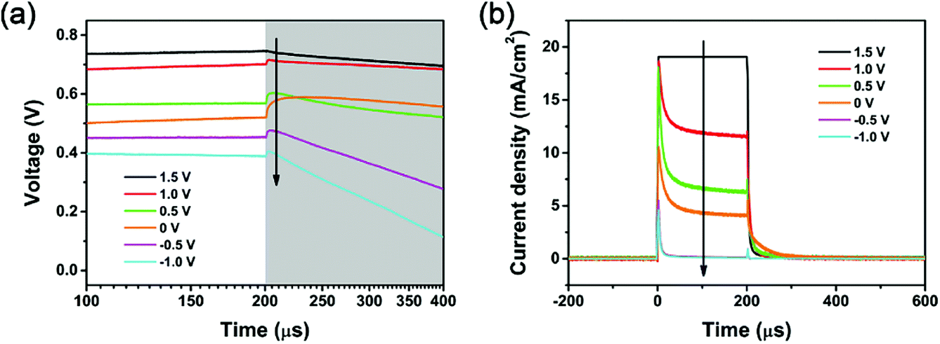 | ||
| Fig. 2 (a) Transient photovoltage and (b) photocurrent responses to single light pulse of the devices pretreated at different biases. | ||
In order to investigate the evolution of transient short-circuit current (TSCC), the TSCC of perovskite solar cells (PerSCs) is measured under the illumination of single light pulse with 200 μs duty time and 100 mW cm−2 intensity. Fig. 3 shows the transient photocurrent responses to the first 10 light pulses of the PerSCs pretreated at 1.5 V and −1.0 V. The interval time between two adjacent pulses is several seconds. Fig. 3a presents the transient photocurrent responses to first ten light pulses of the PerSCs treated at 1.5 V. For the device pretreated at 1.5 V, the amplitude of the transient current response to the first light pulse is closer to the value of short circuit current obtained via I–V curve measurement under the illumination of a standard sun. Then amplitude of the transient current gradually decline with the increase of the number of pulse illumination. Meanwhile, the decay of the transient current in duty time of the pulse illumination progressively aggravate, which means that the accumulation of carriers becomes serious with increasing number of light pulses. Because the ion migration is a slow process, the ion migration can be neglected under the illumination of 200 μs light pulse. The decrease in transient photocurrent might be attributed to the defect induced carrier accumulation.
 | ||
| Fig. 3 Transient photocurrent responses to the first ten light pulses of the device pretreated at 1.5 V (a) and at −1.0 V (b). The inset represents the magnified region of the −1.0 V processed transient photocurrent with the logarithm of the Y axis. | ||
As shown in Fig. 3b, the transient photocurrent of the device pretreated at −1.0 V bias is very low, and slowly rises with increasing number of illumination light pulse. The slow photocurrent rise might come from the redistribution of accumulated ions. Both of ion accumulation and carrier trapping depress transient photocurrent of PerSCs, but the effect of carrier trapping on the transient current is more critical compared with that of ion migration. In addition, the transient short-circuit current responses of the devices pretreated at other biases are shown in Fig. S2.†
As mentioned above, we observe a regular decrease of the transient photocurrent with the number of 200 μs light pulses, while it also decays with increasing time in the duty time of single light pulse, which disagrees with the short-circuit current measured via I–V characteristic curve. In order to investigate the evolution of short circuit current in a long duty time, we measured the transient current of the devices preconditioned at 1.5 V (Fig. 4a–c), 0 V (Fig. 4d–f) and −1.0 V (Fig. 4g–i) by scaling the time from microseconds to hundreds of seconds. It can be seen that the transient photocurrent response under 1.5 V bias pretreatment has a similar trend in the range of microseconds and milliseconds (Fig. 4a and b), while the current response under 0 V and −1.0 V pretreatment conditions exhibits a unusual trend than that under the case of positive bias. The transient photocurrent overshoot behavior can be observed in the microsecond time range (Fig. 4d and g), which is consistent with the results shown above. We measured the transient current under single light pulse with 100 ms duty time. The results show that the short circuit current drops to its minimum in several milliseconds, then gradually rise as shown in Fig. 4e and h.
 | ||
| Fig. 4 The transient photocurrent response from (left to right) microseconds, milliseconds to seconds for the devices pretreated at different biases; (a–c) at 1.5 V, (d–f) at 0 V, (g–i) at −1.0 V. | ||
In order to further illustrate the influence of pretreatment on short circuit current in larger time scale, the time range of measurements are extended to 300 s. In Fig. 4c, f and i, the time dependences of short circuit current of solar cells pretreated at different biases are presented. The time to achieve the maximum of short circuit current drop from about 100 seconds to several seconds when the device pretreatment bias rises from −1.0 V to 1.5 V. From Fig. 4c, we find that the photocurrent of the solar cell pretreated at 1.5 V bias slightly decreases with increasing time and tends to be stable at 50 s, which might indicate that the accumulation ions induced by pretreatment redistribute and achieve a new equilibrium under the new electric field distribution. For the device pretreated at −1.0 V, the time to achieve new ion equilibrium is about 100 s, which is longer than that of device pretreated at 1.5 V. The short circuit current of all devices be stable after about 100 seconds under the illumination of 100 mW cm−2. The stable current density of the devices pretreated at positive biases is slightly higher than that of the devices pretreated at negative biases, which indicates that the influence of pretreatment induced ion accumulation can not eliminated completely. Appropriate electric pretreatment is benefit to the enhancement in the performance of perovskite solar cells.
Normally, the ion migration in perovskite films would happen under the action of intense enough electric field.20,21,24 Some ions would shift to the interface between carrier transport layers and perovskite active layer as well accumulate the area close to the interfaces. The ion accumulation would result in the energy bending and additional electric field which directly influences the carrier dynamics process. The migration of ions are a slow process. It would take tens of seconds to reach the equilibrium of ion distribution.39–41 Herein we use the ion migration induced band bending model to explain above phenomenon induced. In Fig. 5, the band configurations of perovskite layers pretreated at different biases and their evolution are presented. The ion accumulation, trapping and accumulation of carriers influence the band configuration of perovskite layer. Fig. 5a depicts the initial energy band diagram of the device without treatment and illumination and there is no injection barrier at the interface. For the device pretreated at the −1.0 V bias, some anions move toward cathode and accumulate at the interface between perovskite active layer and ETL in pretreatment process (Fig. 5b). The accumulation of anions would induce a barrier at the areas near to the interfaces between perovskite active layer, which would block the transport of electrons and decrease the transient photocurrent during the illumination of the first light pulse. In addition, some photogenerated carriers are trapped by the defects at the interfaces of perovskite and TiOx ETL (as shown in Fig. 5c), which further enhances band bending. Attributing to the anion accumulation and the carrier trapping, a valley of conductive band would form in the area near to the interface between ETL and perovskite active layer. During the light illumination, some electrons would accumulate in the valley, which cause the decrease in short-circuit current and open-circuit voltage. With the increasing number of accumulation electrons, the energy band of electron accumulation area would gradually rise (Fig. 5d). Meanwhile the valley become shallow, and the transient short current would increase. However, the local electric field in the electron accumulation area would become weak even is against the direction of carrier collection, and the transport of electrons would still be hindered. For the device pretreated at 1.5 V bias, as depicted in Fig. 5e, the cations accumulate at the interface between perovskite active layer and ETL, which would cause the band to bend downward in the cations accumulation area near to the interfaces between perovskite active layer. The bending downward of band is benefit to carrier transport and carrier collection. Once illumination is on, as illustrated in Fig. 5f, some photogenerated electrons would be trapped by the defects in the area near to the interface between perovskite layer and ETL. The trapping of electron would overcome the effect of cation accumulation and induce a barrier. The barrier would block the photogenerated electrons to be extracted by cathode, and photocurrent goes down. Similar process also happens at the interface between perovskite layer and spiro-OMeTAD hole transport layer.
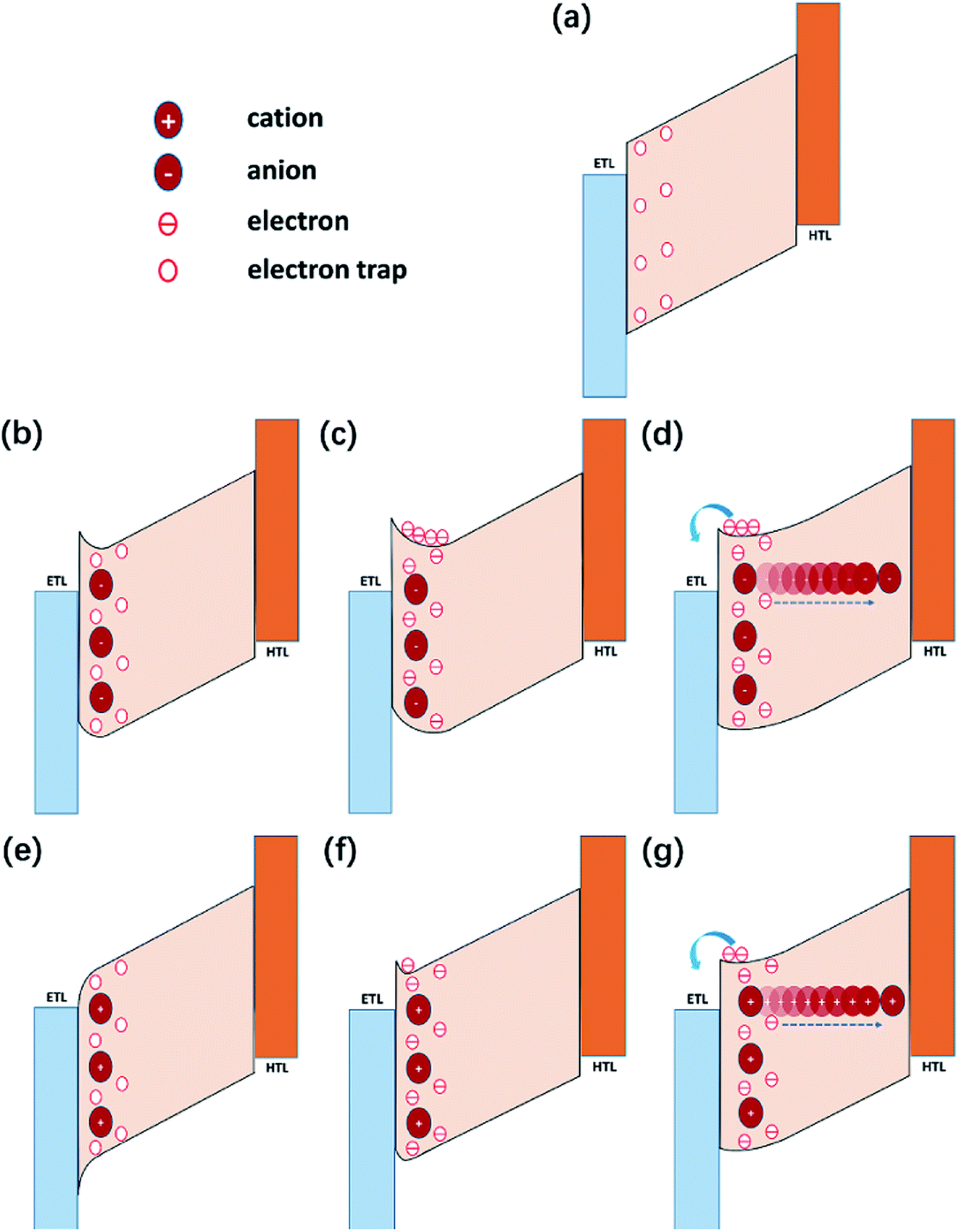 | ||
| Fig. 5 Energy band evolution of perovskite solar cells pretreated at bias negative and large enough positive bias. (a) The initial energy band bending diagram inside the device without treatment and illumination. (b) Negative bias treatment without illumination. (c) Negative bias treatment with illumination. (d) Anion reverse diffusion after negative bias pretreatment. (e) Positive bias treatment without illumination. (f) Positive bias treatment with illumination. (g) Cation reverse diffusion after positive bias pretreatment. | ||
Because the pretreatment bias is removed from the device, the accumulated ions would gradually shift and achieve a new balanced ion distribution. As illustrated in the Fig. 5d and g, the bending of the band induced by ion accumulation would become weak with the ion diffusion. However, the difference in stable photocurrent of the devices pretreated at various biases reveals that the ion distribution of the devices pretreated at high electric field can not come back to that it was. Comparing the impact of carrier trapping and ion migration on the performance, one can conclude that the key issue is defect induced carrier trapping for the perovskite solar cells with compact nano-TiOx film as ETL.
Conclusions
In this paper, the impact of ion migration, carrier trapping and carrier accumulation on the performance of perovskite solar cells with compact nano-TiOx films as electron transport layer are investigated. In order to distinguish the impact of carrier trapping and ion migration on performance of perovskite solar cells, the approaches of single light illumination and electric pretreatment at different biases are employed. Our results reveal that the both of carrier trapping and ion migration are key factors to decide the performance, but the impact from carrier trapping is more crucial for of the perovskite solar cells with compact nano-TiOx films. The pretreatment at positive bias beyond build-in potential can partly compensate the adverse impact of defect induced carrier trapping, which is benefit to enhance the performance of perovskite.Conflicts of interest
There are no conflicts to declare.Acknowledgements
This work was supported by Natural Science Foundation of China (Grants 61775011, 61735004, 61674012, and 61675018).References
- S. D. Stranks, G. E. Eperon, G. Grancini, C. Menelaou, M. J. Alcocer, T. Leijtens, L. M. Herz, A. Petrozza and H. J. Snaith, Science, 2013, 342, 341–344 CrossRef CAS PubMed.
- G. Xing, N. Mathews, S. Sun, S. S. Lim, Y. M. Lam, M. Gratzel, S. Mhaisalkar and T. C. Sum, Science, 2013, 342, 344–347 CrossRef CAS PubMed.
- S. De Wolf, J. Holovsky, S. J. Moon, P. Loper, B. Niesen, M. Ledinsky, F. J. Haug, J. H. Yum and C. Ballif, J. Phys. Chem. Lett., 2014, 5, 1035–1039 CrossRef CAS PubMed.
- W. J. Yin, T. Shi and Y. Yan, Adv. Mater., 2014, 26, 4653–4658 CrossRef CAS PubMed.
- V. D'Innocenzo, G. Grancini, M. J. Alcocer, A. R. Kandada, S. D. Stranks, M. M. Lee, G. Lanzani, H. J. Snaith and A. Petrozza, Nat. Commun., 2014, 5, 3586 CrossRef PubMed.
- A. Miyata, A. Mitioglu, P. Plochocka, O. Portugall, J. T.-W. Wang, S. D. Stranks, H. J. Snaith and R. J. Nicholas, Nat. Phys., 2015, 11, 582–587 Search PubMed.
- G. E. Eperon, S. D. Stranks, C. Menelaou, M. B. Johnston, L. M. Herz and H. J. Snaith, Energy Environ. Sci., 2014, 7, 982–988 RSC.
- J. H. Noh, S. H. Im, J. H. Heo, T. N. Mandal and S. I. Seok, Nano Lett., 2013, 13, 1764–1769 CrossRef CAS PubMed.
- R. Prasanna, A. Gold-Parker, T. Leijtens, B. Conings, A. Babayigit, H. G. Boyen, M. F. Toney and M. D. McGehee, J. Am. Chem. Soc., 2017, 139, 11117–11124 CrossRef CAS PubMed.
- R. A. Belisle, W. H. Nguyen, A. R. Bowring, P. Calado, X. Li, S. J. C. Irvine, M. D. McGehee, P. R. F. Barnes and B. C. O'Regan, Energy Environ. Sci., 2017, 10, 192–204 RSC.
- B. V. Lotsch, Angew. Chem., Int. Ed. Engl., 2014, 53, 635–637 CrossRef CAS PubMed.
- N. J. Jeon, H. Na, E. H. Jung, T.-Y. Yang, Y. G. Lee, G. Kim, H.-W. Shin, S. Il Seok, J. Lee and J. Seo, Nat. Energy, 2018, 3, 682–689 CrossRef CAS.
- Q. Jiang, Y. Zhao, X. Zhang, X. Yang, Y. Chen, Z. Chu, Q. Ye, X. Li, Z. Yin and J. You, Nat. Photonics, 2019, 13, 460–466 CrossRef CAS.
- M. Kim, G.-H. Kim, T. K. Lee, I. W. Choi, H. W. Choi, Y. Jo, Y. J. Yoon, J. W. Kim, J. Lee, D. Huh, H. Lee, S. K. Kwak, J. Y. Kim and D. S. Kim, Joule, 2019, 3, 2179–2192 CrossRef CAS.
- NREL, Research Cell Efficiency Records, http://www.nrel.gov/ncpv/, accessed: October 2019 Search PubMed.
- S. A. L. Weber, I. M. Hermes, S.-H. Turren-Cruz, C. Gort, V. W. Bergmann, L. Gilson, A. Hagfeldt, M. Graetzel, W. Tress and R. Berger, Energy Environ. Sci., 2018, 11, 2404–2413 RSC.
- W. Tress, J. Phys. Chem. Lett., 2017, 8, 3106–3114 CrossRef CAS PubMed.
- G. Richardson, S. E. J. O'Kane, R. G. Niemann, T. A. Peltola, J. M. Foster, P. J. Cameron and A. B. Walker, Energy Environ. Sci., 2016, 9, 1476–1485 RSC.
- D. A. Jacobs, Y. Wu, H. Shen, C. Barugkin, F. J. Beck, T. P. White, K. Weber and K. R. Catchpole, Phys. Chem. Chem. Phys., 2017, 19, 3094–3103 RSC.
- Z. Xiao, Y. Yuan, Y. Shao, Q. Wang, Q. Dong, C. Bi, P. Sharma, A. Gruverman and J. Huang, Nat. Mater., 2015, 14, 193–198 CrossRef CAS PubMed.
- Y. Yuan, J. Chae, Y. Shao, Q. Wang, Z. Xiao, A. Centrone and J. Huang, Adv. Energy Mater., 2015, 5, 1500615 CrossRef.
- T. Pang, R. Jia, Y. Wang, K. Sun, Z. Hu, Y. Zhu, S. Luan and Y. Zhang, J. Mater. Chem. C, 2019, 7, 609–616 RSC.
- Y. Deng, Z. Xiao and J. Huang, Adv. Energy Mater., 2015, 5, 1500721 CrossRef.
- Y. Yuan and J. Huang, Acc. Chem. Res., 2016, 49, 286–293 CrossRef CAS PubMed.
- C. Eames, J. M. Frost, P. R. Barnes, B. C. O'Regan, A. Walsh and M. S. Islam, Nat. Commun., 2015, 6, 7497 CrossRef CAS PubMed.
- J. M. Azpiroz, E. Mosconi, J. Bisquert and F. De Angelis, Energy Environ. Sci., 2015, 8, 2118–2127 RSC.
- L. Bertoluzzi, R. A. Belisle, K. A. Bush, R. Cheacharoen, M. D. McGehee and B. C. O'Regan, J. Am. Chem. Soc., 2018, 140, 12775–12784 CrossRef CAS PubMed.
- P. Lopez-Varo, J. A. Jiménez-Tejada, M. García-Rosell, J. A. Anta, S. Ravishankar, A. Bou and J. Bisquert, ACS Energy Lett., 2017, 2, 1450–1453 CrossRef CAS.
- C. Li, S. Tscheuschner, F. Paulus, P. E. Hopkinson, J. Kiessling, A. Kohler, Y. Vaynzof and S. Huettner, Adv. Mater., 2016, 28, 2446–2454 CrossRef CAS.
- W. Tress, N. Marinova, T. Moehl, S. M. Zakeeruddin, M. K. Nazeeruddin and M. Grätzel, Energy Environ. Sci., 2015, 8, 995–1004 RSC.
- Y. Wu, A. Islam, X. Yang, C. Qin, J. Liu, K. Zhang, W. Peng and L. Han, Energy Environ. Sci., 2014, 7, 2934–2938 RSC.
- Y. J. Jeon, S. Lee, R. Kang, J. E. Kim, J. S. Yeo, S. H. Lee, S. S. Kim, J. M. Yun and D. Y. Kim, Sci. Rep., 2014, 4, 6953 CrossRef CAS PubMed.
- X. Zheng, B. Chen, J. Dai, Y. Fang, Y. Bai, Y. Lin, H. Wei, X. C. Zeng and J. Huang, Nat. Energy, 2017, 2, 17102 CrossRef CAS.
- H. Lei, P. Dai, X. Wang, Z. Pan, Y. Guo, H. Shen, J. Chen, J. Xie, B. Zhang and S. Zhang, Adv. Mater. Interfaces, 2019, 7, 1901716 CrossRef.
- H. Lei, G. Yang, X. Zheng, Z. G. Zhang, C. Chen, J. Ma, Y. Guo, Z. Chen, P. Qin and Y. Li, Sol. RRL, 2017, 1, 1700038 CrossRef.
- H.-S. Kim, I.-H. Jang, N. Ahn, M. Choi, A. Guerrero, J. Bisquert and N.-G. J. T. Park, J. Phys. Chem. Lett., 2015, 6, 4633–4639 CrossRef CAS PubMed.
- G. Xing, B. Wu, S. Chen, J. Chua, N. Yantara, S. Mhaisalkar, N. Mathews and T. C. J. S. Sum, Small, 2015, 11, 3606–3613 CrossRef CAS PubMed.
- C. Li, L. Lv, L. Qin, L. Zhu, F. Teng, Z. Lou, Z. Deng, Y. Hu, Q. Cui and Y. Hou, Materials, 2018, 11(12), 2407 CrossRef PubMed.
- W. Nie, J. C. Blancon, A. J. Neukirch, K. Appavoo, H. Tsai, M. Chhowalla, M. A. Alam, M. Y. Sfeir, C. Katan, J. Even, S. Tretiak, J. J. Crochet, G. Gupta and A. D. Mohite, Nat. Commun., 2016, 7, 11574 CrossRef CAS PubMed.
- E. T. Hoke, D. J. Slotcavage, E. R. Dohner, A. R. Bowring, H. I. Karunadasa and M. D. McGehee, Chem. Sci., 2015, 6, 613–617 RSC.
- Y. Yuan, Q. Wang, Y. Shao, H. Lu, T. Li, A. Gruverman and J. Huang, Adv. Energy Mater., 2016, 6, 1501803 CrossRef.
Footnote |
| † Electronic supplementary information (ESI) available. See DOI: 10.1039/d0ra05082b |
| This journal is © The Royal Society of Chemistry 2020 |