
 Open Access Article
 This Open Access Article is licensed under a Creative Commons Attribution-Non Commercial 3.0 Unported Licence
First-principles study of vacancy defects at interfaces between monolayer MoS2 and Au
Xiaoqian Qiua,
Yiren Wang *a and
Yong Jiangab
*a and
Yong Jiangab
aKey Laboratory for Nonferrous Metal Materials Science and Engineering (MOE), School of Materials Science and Engineering, Central South University, Changsha, 410083, China. E-mail: yiren.wang@csu.edu.cn; yjiang@csu.edu.cn
bState Key Laboratory for Powder Metallurgy, Central South University, Changsha 410083, China
First published on 4th August 2020
Abstract
The performance of MoS2 based devices is closely related to the quality and defect morphology of the monolayer MoS2 deposited on metal. First-principles calculations were performed to investigate the vacancy effects of Au–mMoS2 contact. Four possible S-vacancy and a Mo-vacancy were considered in our calculations. Energetic studies show that S-vacancies are easier to form than Mo-vacancy in Au–mMoS2 contact, while S-vacancy (hollow site at interface, VS4) has the lowest formation energy under Mo-rich environments. Electron and charge redistribution analysis of defective Au–mMoS2 contact indicate that the lower contact resistance and higher electron injection efficiency of defective Au–MoS2 contact than perfect ones. Notably, the S-vacancy at top layer showed better electronic performance than that at bottom layer of monolayer MoS2 in the contact. High quality n-type Au–mMoS2 contact can therefore be expected through defect engineering.
Introduction
The discovery of graphene has upended the traditional understanding of two-dimensional structures, however, the zero-bandgap nature of graphene has limited their digital logic applications.1 Transition-metal dichalcogenides (TMDs) with tunable bandgaps like MoS2, WSe2, etc. have emerged to be potential materials for digital logic applications in spite of their inferior carrier mobility.2 Bulk MoS2 has a graphene-like layered structure, where the S–Mo–S slabs are stacked together via weak van der Waals (vdW) interlayer interaction3 Few-layer MoS2 can therefore be mechanically exfoliated4 and their bandgaps vary with the number of layers.5 Monolayer MoS2 has a direct bandgap of 1.81 eV,6 which endows many excellent properties for nanoelectronics. Monolayer MoS2 has been regarded as a highly competitive candidate for field-effect transistors (FETs) with a high on/off ratio, and photodetectors based on MoS2 have been intensively investigated.7–9A metal contact is required to inject appropriate types of carriers into the host materials for an actual electronic or photoelectronic device using 2D materials as the semiconducting channel.10 Abundant researches11–14 have shown that the properties for 2D materials based devices can be tuned by substrate selections through interlayer interaction. Copper is the most well-studied metal contact for MoS2 based devices. Experimentally, Kim D. et al. prepared monolayer MoS2 islands on a copper surface at moderate growth conditions through sulfur loading of the substrate using thiophenol via e-beam evaporation (physical vapor deposition), and obtained high quality MoS2 monolayer with atomic ordering.15 Later on, first-principles calculations were demonstrated by Le D. et al. to investigate the geometric and electronic structures of monolayer MoS2 on Cu(111).16 They predicted chemical interaction between monolayer MoS2 and the Cu surface atoms instead of physical adsorption.
Au has shown privilege conducting properties, ductility and better interlayer interaction comparing to Cu, is expected to be ideal substrate materials for fabricating monolayer MoS2.17 Large area single-layer MoS2 has been successfully synthesized on the Au(111) surface by physical vapor deposition (PVD) in ultrahigh vacuum.18 It is interesting to note that B. Radisavljevic et al. used a hafnium oxide gate dielectric to demonstrate a room-temperature single-layer MoS2 mobility of at least 200 cm2 V−1 s−1, similar to that of graphene nanoribbons, and demonstrated transistors with room-temperature current on/off ratios of 1 × 10⁸ and ultralow standby power dissipation, where Au as the electrode of the transistors. However, calculations by Popov et al.19 suggested that it is rather inefficient for electron injection from Au into single-layer MoS2 while forming a tunnel barrier at the interface.20 The inefficiency can be caused by the pristine monolayer MoS2 model adopted in their calculations. However, experimental investigation speculated that the low contact resistance between Au and monolayer MoS2 was due to defects of pristine monolayer MoS2 during the preparation process.21
The performance of devices is closely related to the quality and defect morphology of the monolayer MoS2 since defects are evitable during the preparation process. It has been well documented that vacancies in monolayer MoS2 can have significant influence on the electronic and magnetic properties.22–26 In addition, vacancies can introduce dangling bonds at the interface between the monolayer MoS2 and Au, which can enhance adsorption capacity and improve the carrier mobility.10 Su et al.17 studied the effects of vacancies in monolayer MoS2 on electronic structure and electronic properties of Au–MoS2 contact and suggest that defective Au–mMoS2 top contacts have lower contact resistance and higher electron injection efficiency, whereas Au–MoS2 contact with Mo-vacancy shows chemisorption interface with ohmic character. Displacement reaction by reactive metals is energetically favourable, which should act to lower resistance contacts.27 However, their researches ignored the stability of the model. The mismatch between monolayer MoS2 and Au remains large relatively, which may lead to deviations. Only one possible S-vacancy site was concerned in their model, further demonstrations for vacancy effects in Au–MoS2 system are required.
In this study, first-principles calculations are performed to further illustrate the interface effect induced by intrinsic vacancies. Interface model of Au–mMoS2 with a relatively small mismatch is therefore built to investigate the electronic structure and electronic properties of the system of Au–mMoS2 contact. These studies may pave the ways for optimal design of MoS2-based electronic devices.
Computational details
First principles calculations were performed based on the density functional theory (DFT) with local density approximation (LDA). The geometry optimizations and electronic structure calculations are performed with the projector augmented wave (PAW) pseudopotential28 and the plane-wave cutoff energy is set to be 450 eV, implemented in the Vienna ab initio simulation package (VASP) code.29,30 DFT-D2 scheme is included to describe the vdW interactions. The maximum Hellmann–Feynman force between each atom during geometry optimization is less than 0.02 eV Å−1, and energies are converged to within 1.0 × 10⁻⁵ eV per atom. A 5 × 5 × 1 k-mesh based on gamma-centered scheme is applied for relaxation calculations. A vacuum slab of 15 Å is added in monolayer and interface models to avoid spurious interactions between the individual structures. All the calculations were performed under same relaxation criteria and spin-polarized calculations were considered for all defective models.Results and discussion
A (√3 × √3) supercell of monolayer MoS2, consisting of 3 Mo atoms and 6 S atoms with one Mo layer arrays between two S layers in a trigonal prismatic layout, is adopted in this study.The calculated lattice constant of monolayer is 3.160 Å, which is in excellent consistent with the experimental value (3.161 Å).31 and the calculated average Mo–S bond length is 2.374 Å. The calculated band gap for pristine monolayer MoS2 is 1.87 eV, as illustrated in Fig. 1b, agreeing well with the experimental value (1.90 eV).6 The schematic of metal–mMoS2 transistor device is shown in Fig. 2a. Testified four layers of Au atoms were chosen to simulate the metal contact and a 2 (√3 × √3) monolayer MoS2 (see Fig. 1a) was absorbed on one side of the Au (111) surfaces, as shown in Fig. 2b and c. The lattice constants of Au (111) surface are kept fixed to simulate the experimental deposition environment, with a = b = 3.122 Å. Fig. 3a–e show the models of Au–mMoS2 with five concerned vacancies after structural relaxation.
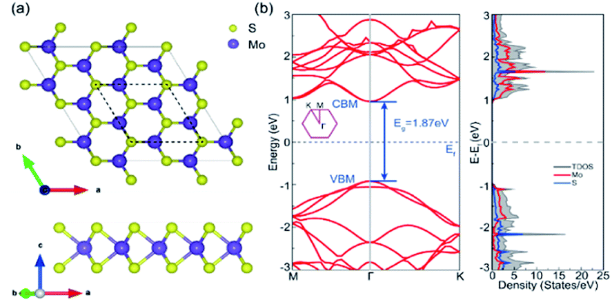 | ||
| Fig. 1 (a) The atomic structures of monolayer MoS2 from top view and side view, the dotted lines represent the calculated √3 × √3 cell. (b) Band structure and DOS of monolayer MoS2 in a √3 × √3 cell. | ||
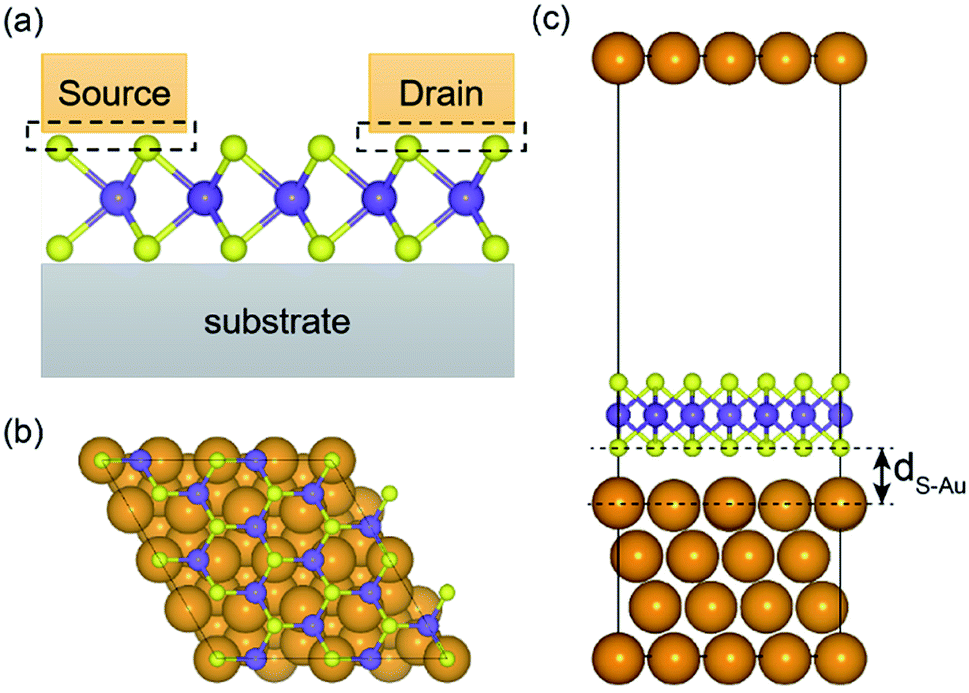 | ||
| Fig. 2 (a) 2D cross-section schematic of metal–mMoS2 transistor devices; structural diagram of Au–mMoS2 contact: (b) the top view; (c) the side view, dS–Au represents the vertical average distance monolayer MoS2 and Au. | ||
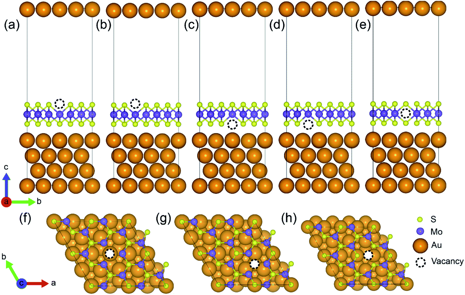 | ||
| Fig. 3 Schematic diagram of Au–mMoS2 top contact with (a)–(d) S-vacancy and (e) Mo-vacancy: VS1, VS2, VS3, VS4 and VMo; (f) corresponds to the top view of (a) and (c); (g) corresponds the top view of (b) and (d); and (h) is the top view of (e). | ||
The structural effects for different types of vacancies on the Au–mMoS2 can be evaluated by calculating average bond lengths of Mo–S and atomic layer spacing dS–Au (as denoted in Fig. 2), which are summarized in Table 1. It can be found that the covalent bond length of Mo–S is slightly increased when contact with Au comparing to pristine monolayer. Moreover, it is obvious that both bond lengths and dS–Au (see Fig. 2) with defects are shorter than pristine systems. The shrink can be owed to the surrounding atoms move outwards when a vacancy forms.23 The formation of either Mo or S vacancy can facilitate the adsorption of gold with monolayer MoS2 since interface distances are generally decreased.
| Structure | Mo–S (Å) | dS–Au (Å) |
|---|---|---|
| mMoS2 | 2.378 | — |
| Au–mMoS2 | 2.432 | 2.820 |
| VS1 | 2.387 | 2.811 |
| VS2 | 2.387 | 2.814 |
| VS3 | 2.386 | 2.811 |
| VS4 | 2.387 | 2.808 |
| VMo | 2.408 | 2.443 |
The structural stability of different vacancies defects can be calculated using the following equation,22
| Ef = Evacancy − Eperfect + ∑Ni × μi |
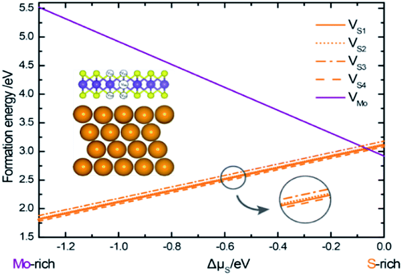 | ||
| Fig. 4 Formation energies of different vacancies as functions of sulfur chemical potential, plotted in the range −1.3 eV ≤ Δμs ≤ 0 eV, corresponding to the formation of bulk Mo and bulk alpha-S. | ||
The slopes of the energy profiles are proportional to the excess/deficit of S atoms in the defects. It can be seen that with the increase of the sulfur content, the formation energy of a Mo-vacancy in the Au–mMoS2 contact decreases linearly. This implies that Mo-vacancy is more likely to form under S-rich environment. Similarly, the Au–mMoS2 with a S-vacancy can be more stable under Mo-rich condition. In addition, the formation energies of four types of S-vacancies can be relatively lower than that of Mo-vacancy under a wide range of sulfur chemical potentials. In most cases, it is easier to form S-vacancy in Au–mMoS2 top contact than Mo-vacancy. VS4 at interface hollow site has the lowest formation energy among the four concerned S-vacancies under Mo-rich environments. The variations in formation energies of a (Mo or S) vacancy in the Au–mMoS2 contact are consistent with those of a (Mo or S) vacancy in monolayer MoS2.31 The actual experimental conditions of growth for MoS2 deposited on gold is assumed to be the Mo-rich region since experimental results have shown a sub-stoichiometric Mo/S ratio higher than 0.5, suggesting a loss of S atoms.33 Formation energies for double S-vacancies (V2S) are calculated using the same equation. Five different configurations of V2S with various vacancy distances are considered. The calculated formation energy of V2S is roughly twice of a single VS, suggesting weak tendency of dimerization of S-vacancies under the Mo-rich conditions.
The partial density of states (PDOS) projection onto Au, S and Mo atom orbits are presented in Fig. 5a–f for the perfect and defective Au–mMoS2 contact (VMo, VS1, VS2, VS3, and VS4) to investigate the effect of vacancies on the electronic properties. We selected the Au atoms at the interface to eliminate the influence of the Au atoms in the bulk phase. It can be found that the top of the valence bands and the bottom of the conduction bands of monolayer MoS2 are dominated by the hybridization of anti-bonding and bonding between Mo_4d and S_3p states. Upon contact with Au, both Mo_4d and S_3p states of monolayer MoS2 (in Fig. 1b) are shifted almost 0.3 eV in the direction of negative axis and spread across the original band gap of pristine monolayer MoS2. Besides, Fermi level is mainly occupied by Mo_4d states, where PDOS corresponds to a low carrier density. No obvious overlap of the concerned interfacial orbitals can be found near the Ef, indicating weak bonding between interfacial atoms. A physisorption of Au/MoS2 interface is predicted.
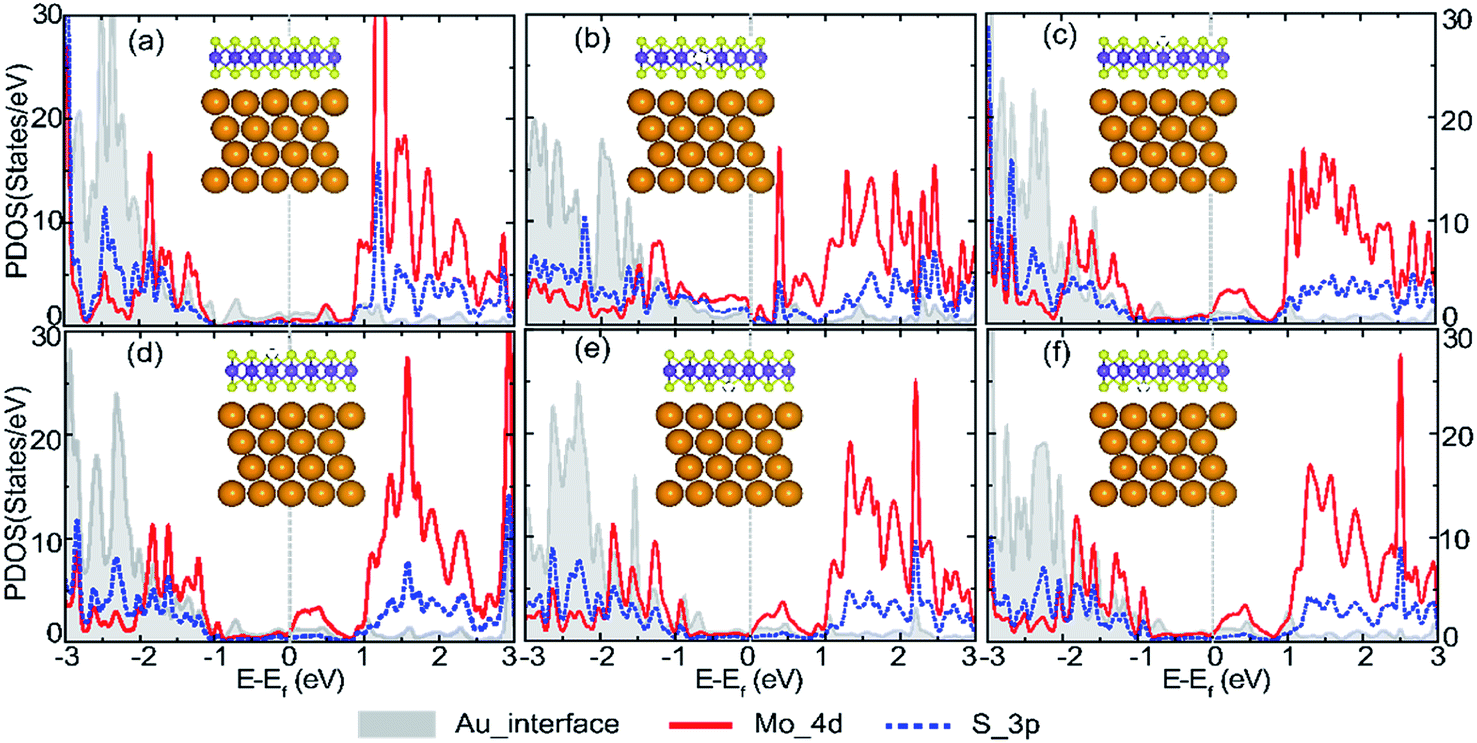 | ||
| Fig. 5 Calculated PDOS of (a) perfect Au–mMoS2 contact, (b) VMo, (c) VS1, (d) VS2, (e) VS3, and (f) VS4. The fermi levels are set at zero level as denoted by dashed grey lines. | ||
Defect energy levels can be introduced when there is a vacancy. Strong interaction between S_3p and Au_5d states is observed in Au–mMoS2 contact with a Mo-vacancy, (Fig. 5b) which implies a higher electron injection efficiency compared to a perfect Au–mMoS2 contact. Furthermore, some peaks of the PDOS occur near the top of original valence bands of the monolayer MoS2, indicating the defective contact is p-type. Fig. 5c–f illustrate the PDOS of Au–mMoS2 contact with different types of S-vacancies. There is no evident difference of the PDOS when S-vacancy locates in the same atomic layer. However, stronger hybridization between S_3p and Au_5d orbitals of S-vacancy in top S layer (VS1 or VS2) is found than that of vacancies in bottom layer of monolayer MoS2 (VS3 or VS4). A n-type Au–mMoS2 contact is expected with all kinds of S-vacancies.
Band structure analysis on selected atoms of perfect and defective Au–mMoS2 contact are shown in Fig. 6. Despite the energy bands of MoS2 and Au are mostly hybridized together, the majority bands of the MoS2 can be recognized clearly. The monolayer MoS2 still presents semiconducting nature in the perfect contact as shown in Fig. 6a, further confirming the physisorption of the Au/MoS2 interface. However, the Fermi level of the Au–mMoS2 generally moves upward and the bad gap slightly reduces comparing with single monolayer MoS2. Fig. 6b–e present the band structures of four types of Au–mMoS2 contact with S-vacancy. It is obvious that defect bands can be introduced and band gap shall be reduced, therefore stronger interaction between Au and monolayer MoS2 than pristine contact is expected. Fermi levels of the defective contact always lie in the band gap region of MoS2, contributing to the formation of Schottky barrier heights, which can be evaluated by the energy differences between the conduction band minimum and the Fermi levels. VS1 and VS2 located at the top layer are predicted to have smaller band gap and lower Schottky barrier heights at interface than the bottom vacancies due to stronger hybridization of interfacial Au and MoS2. Au–mMoS2 contact with a Mo-vacancy has a narrower and more active band gap than S-vacancies as shown in Fig. 6f and better chemical contact with substrate is therefore expected.
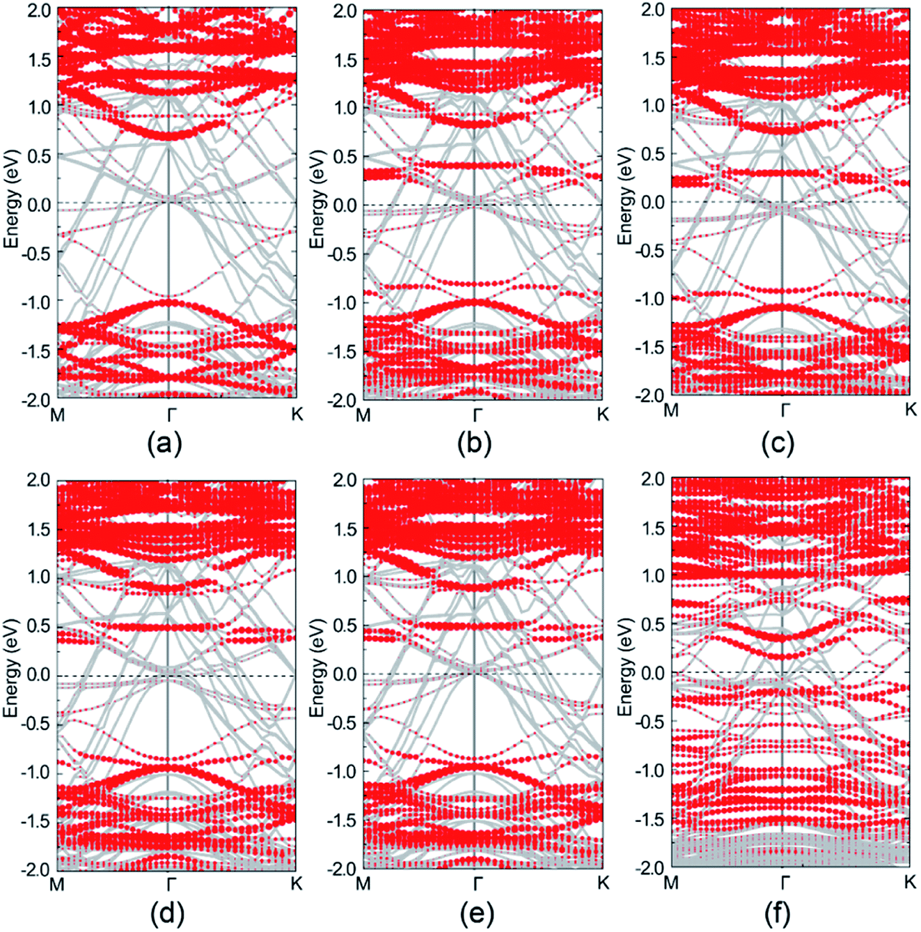 | ||
| Fig. 6 Band structure of Au–mMoS2 and Au–mMoS2 with detects. (a) Represents perfect Au–mMoS2; (b)–(f) correspond to VS1, VS2, VS3, VS4 and VMo, respectively. Fermi level is at zero energy; the grey lines and red dotted lines represent the total band structure and contributions from MoS2, respectively. | ||
To further illustrate the interfacial bonding and electronic properties, the total electron distributions of the Au–mMoS2 contacts were plotted in Fig. 7. Electron redistributions can be observed around the defective areas, which result in stronger binding between the monolayer and substrate. The electron accumulations around interfacial S and Au atoms in defective contacts imply a transition from physisorption into chemisorption and formation of weak Au–S covalent bonds. The Au–S bonds in system with Mo-vacancy is more covalent than others, consisted with their band structure analysis. The defective systems can therefore exhibit higher electron injection efficiency than pristine ones.
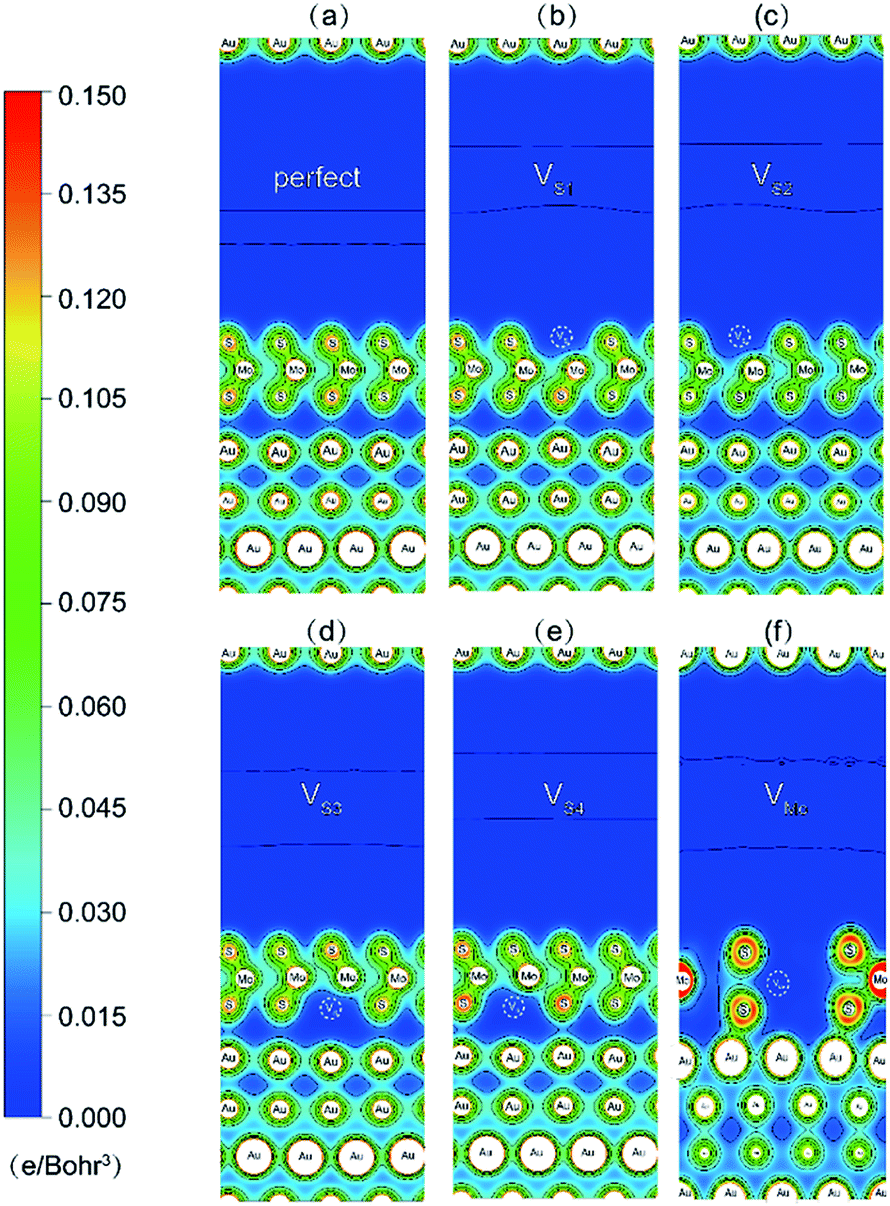 | ||
| Fig. 7 Contour plots of total charge density of Au–mMoS2 contact: (a) perfect Au–MoS2 contact, (b)–(e) defective Au–MoS2 contact with various S-vacancy. (f) Defective Au–MoS2 contact with a Mo-vacancy. | ||
Conclusions
In summary, the interfacial properties of Au–mMoS2 contact with possible vacancies were systematically investigated through first-principles calculations. Based on the afore discussed results, we found that the formation energies of four types of S-vacancy are generally lower than Mo-vacancy over a wide range of S chemical potential. The actual experimental growth condition is assumed to be Mo-rich where S-vacancies are more likely to form. Density of states, band structures and electron density of states analysis of the systems indicate a lower contact resistance and higher electron injection efficiency of defective Au–MoS2 contacts than perfect one. Notably, the S-vacancy locates on the top layer of monolayer MoS2 shows better performance than that on the bottom layer. Mo-vacancy is beneficial for obtaining high quality p-type Au–mMoS2 contact, whereas n-type contacts can be achieved by S-vacancies. These findings can bring new ideas for design and fabrication of novel nanoelectronics devices with monolayer MoS2 through defect engineering.Conflicts of interest
There are no conflicts to declare.Acknowledgements
The authors would like to thank the financial support from the Natural Science Foundation of Hunan Province (No. 2019JJ50795). The computational resource at the High-Performance Computing Center of Central South University is also gratefully acknowledged.References
- V. Singh, D. Joung, L. Zhai, S. Das, S. I. Khondaker and S. Seal, Prog. Mater. Sci., 2011, 56, 1178–1271 CrossRef CAS
.
- D. Saha and S. Mahapatra, Appl. Phys. Lett., 2016, 108, 253106 CrossRef
- M. Kin Fai, K. He, J. Shan and T. F. Heinz, Nat. Nanotechnol., 2018, 7, 494–498 Search PubMed
- K. S. J. Novoselov, D. Schedin, F. Booth, T. J. Khotkevich, V. V. Morozov, S. V. Morozov and A. K. Geim, Proc. Natl. Acad. Sci. U. S. A., 2005, 102, 10451–10453 CrossRef CAS PubMed
- J. Mann, Q. Ma, P. Odenthal, M. Isarraraz, D. Le, E. Preciado, D. Barroso, K. Yamaguchi, G. Palacio, A. Nguyen, T. N. Tai, M. Wurch, A. Nguyen, V. Klee, S. Bobek, D. Sun, T. Heinz, T. Rahman, R. Kawakami and L. Bartels, Adv. Mater., 2014, 26, 1399–1404 CrossRef CAS PubMed
- K. Mak, C. Lee, J. Hone, J. Shan and T. Heinz, Phys. Rev. Lett., 2010, 105, 136805 CrossRef PubMed
- W. Zhang, J.-K. Huang, C.-H. Chen, Y.-H. Chang, Y.-J. Cheng and L. Li, Adv. Mater., 2013, 25, 3456–3461 CrossRef CAS PubMed
- X. Wang, P. Wang, J. Wang, X. Zhou, N. Guo, H. Huang, S. Sun, H. Shen, T. Lin, M. Tang, L. Liao, A. Jiang, J. Sun, X. Meng, X. Chen, W. Lu and J. Chu, Adv. Mater., 2015, 27, 6575–6581 CrossRef CAS PubMed
- Y. Chen, X. Wang, P. Wang, H. Huang, G. Wu, B. Tian, Z. Hong, Y. Wang, S. Sun, H. Shen, J. Wang, W. Hu, J. Sun, X. Meng and J. Chu, ACS Appl. Mater. Interfaces, 2016, 8, 32083–32088 CrossRef CAS PubMed
- J. Kang, W. Liu, D. Sarkar, D. Jena and K. Banerjee, Phys. Rev. X, 2014, 4, 031005 Search PubMed
- H. Zhong, R. Quhe, Y. Wang, Z. Ni, M. Ye, Z. Song, Y. Pan, J. Yang, L. Yang and M. Lei, Sci. Rep., 2016, 6, 21786 CrossRef CAS PubMed
- A. Chanana and S. Mahapatra, J. Appl. Phys., 2014, 116, 204302 CrossRef
- Y. Pan, Y. Wang, M. Ye, R. Quhe, H. Zhong, Z. Song, X. Peng, D. Yu, J. Yang and J. Shi, Chem. Mater., 2016, 28, 2109 Search PubMed
- C. M. Smyth, R. Addou, S. Mcdonnell, C. L. Hinkle and R. M. Wallace, J. Phys. Chem. C, 2016, 120, 14719–14729 CrossRef CAS
- D. Kim, D. Sun, W. Lu, Z. Cheng, Y. Zhu, D. Le, T. S. Rahman and L. Bartels, Langmuir, 2011, 27, 11650–11653 CrossRef CAS PubMed
- D. Le, D. Sun, W. Lu, L. Bartels and T. S. Rahman, Phys. Rev. B: Condens. Matter Mater. Phys., 2012, 85, 075429 CrossRef
- J. Su, N. Li, Y. Zhang, L. Feng and Z. Liu, AIP Adv., 2015, 5, 077182 CrossRef
- S. S. Grønborg, S. Ulstrup, M. Bianchi, M. Dendzik, C. E. Sanders, J. V. Lauritsen, P. Hofmann and J. A. Miwa, Langmuir, 2015, 31, 9700–9706 CrossRef PubMed
- I. Popov, G. Seifert and D. Tománek, Phys. Rev. Lett., 2012, 108, 156802 CrossRef PubMed
- B. Radisavljevic, A. Radenovic, J. Brivio, V. Giacometti and A. Kis, Nat. Nanotechnol., 2011, 6, 147–150 CrossRef CAS PubMed
- C. Maurel, F. Ajustron, R. Péchou, G. Seine and R. Coratger, Surf. Sci., 2006, 600, 442–447 CrossRef CAS
- Y. Wang, L.-T. Tseng, P. P. Murmu, N. Bao, J. Kennedy, M. Ionesc, J. Ding, K. Suzuki, S. Li and J. Yi, Mater. Des., 2017, 121, 77–84 CrossRef CAS
- L.-p. Feng, J. Su and Z.-t. Liu, J. Alloys Compd., 2014, 613, 122–127 CrossRef CAS
- Y. Han, J. Zhou and J. Dong, Appl. Surf. Sci., 2015, 346, 470–476 CrossRef CAS
- D. Ma, W. Ju, T. Li, X. Zhang, C. He, B. Ma, Y. Tang, Z. Lu and Z. Yang, Appl. Surf. Sci., 2016, 364, 181–189 CrossRef CAS
- X. Zhao, C. Xia, T. Wang and X. Dai, Solid State Commun., 2015, 220, 31–35 CrossRef CAS
- D. Liu, Y. Guo, L. Fang and J. Robertson, Appl. Phys. Lett., 2013, 103, 183113 CrossRef
- G. Kresse and D. Joubert, Phys. Rev. B: Condens. Matter Mater. Phys., 1999, 59, 1758–1775 CrossRef CAS
- G. Kresse, J. Non-Cryst. Solids, 1995, 192–193, 222–229 CrossRef
- G. Kresse and J. Furthmüller, Phys. Rev. B: Condens. Matter Mater. Phys., 1996, 54, 11169–11186 CrossRef CAS PubMed
- B. Schonfeld, J. J. Huang and S. C. Moss, Acta Crystallogr., Sect. B: Struct. Sci., 1983, 39, 404–407 CrossRef
- M. V. Bollinger, K. W. Jacobsen and J. K. Nørskov, Phys. Rev. B: Condens. Matter Mater. Phys., 2003, 67, 085410 CrossRef
- M. Donarelli, F. Bisti, F. Perrozzi and L. Ottaviano, Chem. Phys. Lett., 2013, 588, 198–202 CrossRef CAS
| This journal is © The Royal Society of Chemistry 2020 |