
 Open Access Article
 This Open Access Article is licensed under a Creative Commons Attribution-Non Commercial 3.0 Unported Licence
Strain forces tuned the electronic and optical properties in GaTe/MoS2 van der Waals heterostructures†
Yuan Li a,
Jijian Liua,
Xiuwen Zhaoa,
Xingzhao Yuanb,
Guichao Hua,
Xiaobo Yuan*a and
Junfeng Ren*a
a,
Jijian Liua,
Xiuwen Zhaoa,
Xingzhao Yuanb,
Guichao Hua,
Xiaobo Yuan*a and
Junfeng Ren*a
aSchool of Physics and Electronics, Shandong Normal University, Jinan, 250358, China. E-mail: yxb@sdnu.edu.cn; renjf@sdnu.edu.cn
bShandong Management University, Jinan 250376, China
First published on 2nd July 2020
Abstract
Two-dimensional (2D) van der Waals heterostructures (vdWHs) have attracted widespread attention in fundamental materials science and device physics. In this work, we report a novel GaTe/MoS2 vdWH and theoretically investigate the electronic and optical properties based on first-principles calculations. GaTe/MoS2 vdWH possesses an indirect band gap with type-II band alignment. Meanwhile, the interfacial charge transfer from MoS2 to GaTe can effectively separate electrons and holes. Also, this vdWH shows improved visible-ultraviolet optical absorption properties compared with those of the isolated GaTe or MoS2 monolayers. More remarkably, the biaxial strain can not only modulate the band gap but also enhance the optical performance in GaTe/MoS2 vdWH. In particular, the tensile strain is more effective for improving the optical absorption in the visible light region. These findings indicate that GaTe/MoS2 vdWH is a promising candidate for nanoelectronics and optoelectronic devices.
1. Introduction
Since graphene was firstly synthesized experimentally,1 two-dimensional (2D) layered materials have received widespread attention in nanoelectronics and optoelectronic devices for their excellent physical properties.2–4 So far, a wide variety of 2D materials have been extensively studied theoretically and experimentally, such as silicene, stanene, phosphorene, MXenes, transition metal dichalcogenides (TMDCs), and so on.5–7 Inspired by the successful isolation of various 2D materials, the van der Waals heterostructures (vdWHs) composed of two 2D materials have attracted intensive research interest, especially for vdWHs composed of two TMDC monolayers.8–10 Various vdWHs with different electronic structures have been thoroughly studied, and different novel 2D application devices, such as vertical transistors, solar cells, resonant tunneling diodes, and photodetectors, have been reported.11–13 It is well known that the function of the vdWHs deepens largely on their band structures. The separation of electrons and holes into different layers can avoid electron–hole recombination if the vdWHs have type-II band arrangement, which is very useful for the photocatalysis of unipolar electronic devices.13,14 Thus, it is necessary to explore new vdWHs to satisfy the multiple device design demands.Recently, a novel heterostructure composed of group IIIA monochalcogenides and TMDCs have shown great potential in optoelectronic applications. For example, Li et al. reported that a heterostructure composed of GaSe and MoS2 can effectively transport and separate photo-generated charge carriers between layers, resulting in an excellent photovoltaic response.15 Zhang et al. found that the band alignment of the InSe/MoS2 vdWHs can be controlled by applying external strain for photocatalysis.16 Meanwhile, Lei et al. revealed another novel WTe2/HfS2 vdWHs, in which the electronic features can be modulated by applying external strain and electric field.17 All the above results indicate that vdWHs composed of 2D monochalcogenides and TMDCs monolayers may have great potentials in practical applications.
TMDCs are promising building blocks for the new vdWHs. Among those TMDCs, MoS2 is one of the very good semiconductor materials. MoS2 has a direct band gap of 1.8 eV, a high on/off current ratio of 108, a high carrier mobility of 200 cm2 V−1 s−1 at room temperature and outstanding mechanical properties.18 These properties indicate that 2D monolayer MoS2 has potential advantages in the fields of nanoelectronics and optoelectronics. On the other hand, the group IIIA monochalcogenides MX (M = Ga or In, X= S, Se, or Te) are emerging 2D materials, which have been aroused great research attention in future optoelectronic devices.19–21 Among these diverse MX materials, GaTe monolayer has attracted increasing interest owing to its excellent structural, electronic, optical and photocatalytic properties.22,23 The GaTe monolayer has been successfully synthesized by using molecular beam epitaxy or vapor phase deposition methods.24,25 Huang et al. found that the GaTe monolayer with an indirect-band gap is a potential photocatalyst for water splitting, which is a promising solution for generating clean renewable energy.23 Chitara et al. demonstrated that GaTe has good thermoelectric properties and high photo-responsivity (104 A W−1), which are better than single-layer graphene.26
vdWHs composed with MoS2 and GaTe have great potential applications based on their distinct properties. Especially, Wang et al. recently experimentally fabricated GaTe/MoS2 vdWHs by mechanical exfoliation and targeted transfer method, which shows a high photovoltaic and photo-detecting performance.27 Therefore, it is interesting to theoretically understand the physical properties in GaTe/MoS2 vdWHs. In this work, by using the first-principles calculations, we investigate the physical properties of GaTe/MoS2 vdWHs, including the geometric structure, electronic and optical properties, etc. The structure of the article is as follows: the theoretical calculation methods are shown in Section 2, the results analysis is given in Section 3, and a conclusion is listed in Section 4.
2. Methods
First-principles calculations are performed by using the density functional theory (DFT) approach as implemented in the Vienna ab initio Simulation Package (VASP) code with the projector-augmented-wave (PAW) method.28–30 For the exchange and correlation energies, the generalized gradient approximation (GGA) in the form of Perdew–Burke–Ernzerhof (PBE) functional is adopted.31 The DFT-D2 method advanced by Grimme is used to describe the weak vdW interaction between the two monolayers in all calculations.32 The first Brillouin-zone sampling of 5 × 5 × 1 and 9 × 9 × 1 k-points generated by Monkhorst–Pack scheme33 are used for geometric optimization and optical property calculations, respectively. The vacuum layer is set to 20 Å along the Z direction to avoid the interactions induced by the periodic effects. To find a balance between accuracy and efficiency, a 400 eV cut-off energy has been adopted in all calculations. The convergence of the total energy is considered achievable until the energy is less than 10−4 eV and the Hellmann–Feynman force on each atom is 0.01 eV Å−1. It should be pointed out that Mo-based and Te-based materials show the strong spin-orbital couplings (SOC),34,35 however, we mainly focus on the effects of the strain forces on the band structure and the optical properties in GaTe/MoS2 heterostructure in this work, so SOC is not included in the following calculations.In order to study the optical absorption property of GaTe and MoS2 monolayers as well as the GaTe/MoS2 vdWH, the dielectric constant formula need to be obtained. The frequency dependent complex dielectric function is formed by adding the real and imaginary parts as follows,
| ε(ω) = ε1(ω) + iε2(ω) | (1) |
The imaginary part ε2(ω) can be obtained by summing up enough empty band states by the following formula,36
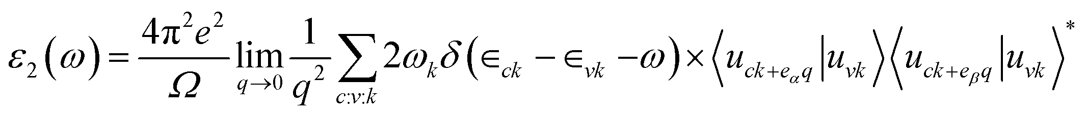 | (2) |
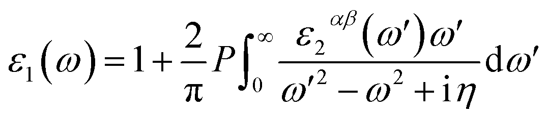 | (3) |
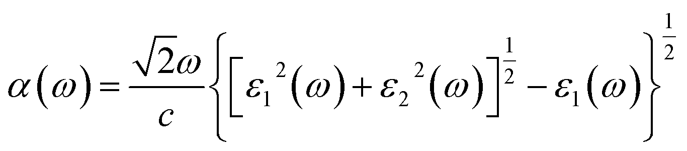 | (4) |
3. Results and discussion
Before studying the properties of the GaTe/MoS2 vdWH, we first consider the structural and electronic properties of the GaTe and MoS2 monolayers. The GaTe monolayer has the hexagonal lattice with a repeating unit of Te–Ga–Ga–Te sequence via covalent bonds, and the calculated lattice parameters are a = b = 4.13 Å. The bond lengths of the Te–Ga and Ga–Ga bonds are dTe–Ga = 2.71 Å and dGa–Ga = 2.47 Å, which agree with the previous theoretical and experimental results.22 MoS2 monolayer also presents hexagonal structures, and the intralayer atoms are sandwiched in the order of S–Mo–S. The lattice constants of MoS2 are a = b = 3.17 Å, which agree with the reported literatures.18 In order to minimize the lattice mismatch value of the vdWH of 1.51%, we utilized a 2 × 2 GaTe supercell and a MoS2 supercell to construct the GaTe/MoS2 vdWH.
To discuss the stacking pattern effects in the GaTe/MoS2 vdWH, four kinds of possible stacking configurations are considered, which are shown in Fig. 1. Te atom locates at the top site of S atom, Te atom locates at the top site of Mo atom, Ga atom locates at the top site of S atom, Ga atom locates at the top site of Mo atom, respectively. All the configurations are completely relaxed. It is clear that both GaTe and MoS2 monolayers maintain their original structures without significant deformations. In order to compare the relatively structural stability of GaTe/MoS2 vdWH, we calculate the binding energies Eb between the GaTe and MoS2 monolayers from the formula Eb = Etotal − EGaTe − EMoS2, where Etotal, EGaTe and EMoS2 are the total energies of GaTe/MoS2 vdWH, the pristine GaTe and MoS2 monolayers, respectively. The calculated binding energies for the four different stacking conformations are −13.58 meV, −16.65 meV, −12.32 meV and −16.28 meV, respectively. The calculated results indicate that GaTe and MoS2 monolayers can form thermodynamically stable GaTe/MoS2 vdWHs. Among them, it is found that the binding energy will be the lowest when the Te atom locates at the top site of Mo atom, which means that this stacking pattern is the most stable one. Meanwhile, the optimized equilibrium distance between GaTe and MoS2 monolayers is 3.56 Å, which is defined as the interlayer height difference between the nearest Te (top-layer) and Mo (lower-layer) atoms. In the following studies, only the most stable configuration is considered.
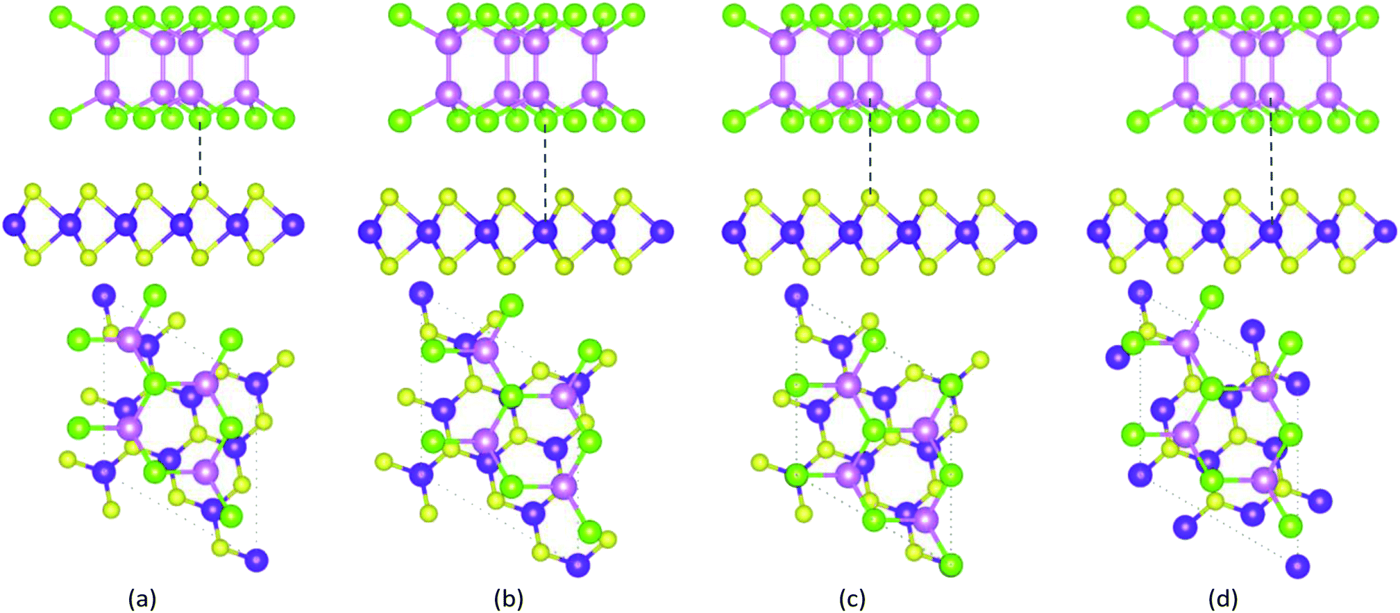 | ||
| Fig. 1 The top and side views of four stacking patterns of the GaTe/MoS2 vdWHs. Pink, green, purple and yellow balls represent Ga, Te, Mo and S atoms, respectively. | ||
Fig. 2(a) and (b) present the electronic band structures of the isolated GaTe and MoS2 monolayers. One can observe that both GaTe and MoS2 monolayers are semiconductors. The GaTe monolayer, as shown Fig. 2(a), has an indirect band gap of 1.42 eV. Its conduction band minimum (CBM) locates at the Γ point, while its valence band maximum (VBM) locates at the Γ–M path in the two-dimensional hexagonal Brillouin zone. In contrast, the MoS2 monolayer has a direct band gap of 1.75 eV, which is coming from both the CBM and VBM at the K point. After combining GaTe and MoS2 monolayers together, we plot the band structures of GaTe/MoS2 vdWH, which are shown in Fig. 2(c). Based on the orbital characteristics, the band structures are plotted by using different colors. It can be seen that the CBM and the VBM of the vdWH are contributed from the MoS2 and GaTe layers, respectively. Thus, this GaTe/MoS2 vdWH has an indirect band gap of 1.26 eV with an inherent type-II band alignment, namely, in which both the valence and the conduction band edges of the GaTe monolayer are higher in energy than the corresponding bands of the MoS2 monolayer. The type-II band alignment can effectively promote the spontaneous separation of the electron–hole pairs and make it a good candidate for various optoelectronics and solar energy conversion devices. Additionally, to get deep insight into the electronic properties of these system, we further examine their density of states (DOS). As depicted in Fig. 2(c), the projected DOS (PDOS) of GaTe/MoS2 shows that the CBM mainly derives from the Mo-4d and S-3d of MoS2, whereas the VBM mostly contains the 4p orbitals of Ga and 5p orbitals of Te in GaTe, which further reveal the type-II characteristics of the vdWH.
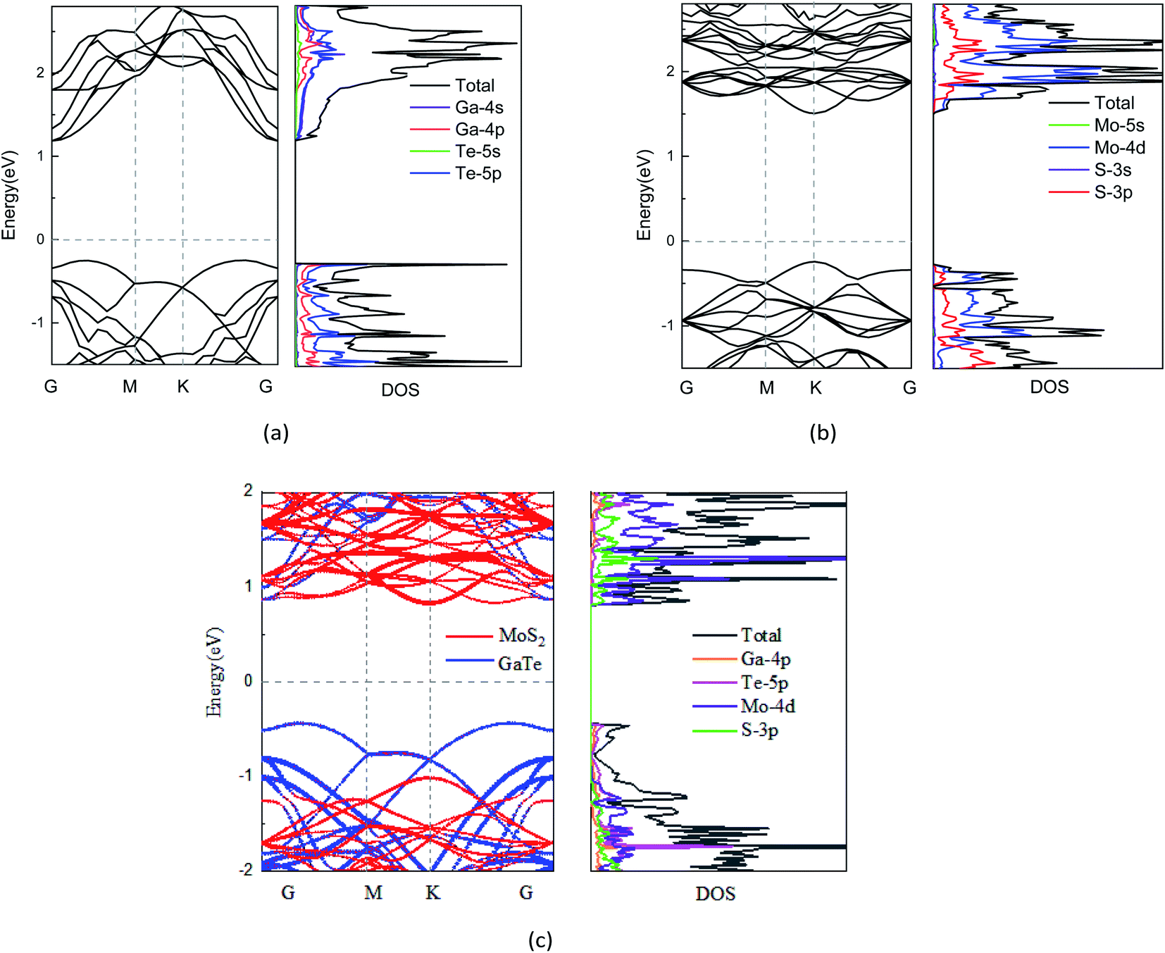 | ||
Fig. 2 Band structure and PDOS of (a) 2 × 2 GaTe monolayer, (b)  MoS2 monolayer, and (c) GaTe/MoS2 vdWH, respectively. MoS2 monolayer, and (c) GaTe/MoS2 vdWH, respectively. | ||
Fig. 3(a) shows the electrostatic potential of the GaTe/MoS2 vdWH at equilibrium distance along the z-direction in its stacking configurations. It can be seen that there is a large electrostatic potential difference between MoS2 and GaTe, in which the MoS2 has a deeper potential than that of the GaTe monolayer. Such different electrostatic potential phenomenon indicates the presence of strong electrostatic field, which may largely influence the carrier dynamics and charge injection. The difference in electrostatic potential indicates the charge transfers from the higher potential layer to the deeper potential layer. Thus, it is apparent that electrons are likely to be driven from the MoS2 layer to the GaTe layer, resulting in the enrichment of holes in MoS2 and the accumulation of electrons in GaTe. To deeper understand the innate character of the charge transfer in the GaTe/MoS2 vdWH, we also investigate the charge density difference, which is calculated as Δρ = ρHetero − ρGaTe − ρMoS2. The results are shown in Fig. 3(b). Here ρHetero is the total charge density of GaTe/MoS2 vdWH, ρGaTe and ρMoS2 are the charge densities of the GaTe monolayer and MoS2 monolayer, respectively. The difference in charge density clearly indicates that by forming the electron-rich and hole-rich regions, the charge density is redistributed. And from Fig. 3(b), it can be clearly seen that the electrons transfer from MoS2 to GaTe, where the red area represents the accumulation of electrons and the blue area represents the depletion of electrons.
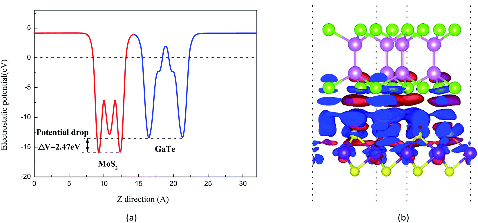 | ||
| Fig. 3 (a) Electrostatic potential along z-direction of the GaTe/MoS2 vdWH. The red and blue lines represent the MoS2 and GaTe. (b) Charge density distributions of the GaTe/MoS2 vdWH at the equilibrium state. The red and blue area represent the electron accumulation and depletion, respectively. The isosurface value is set to be 0.0003 V Å−1. | ||
In order to achieve efficient applications in optoelectronic vdWH materials, we calculated the optical properties for the isolated GaTe and MoS2 monolayers as well as GaTe/MoS2 vdWH. In Fig. S1 in the ESI,† we calculate the dielectric constants ε(ω) of the system and we found that the GaTe/MoS2 vdWH has the largest dielectric constant compared with that of the monolayers in the visible region. As shown in Fig. 4, it is noted that both GaTe and MoS2 monolayers can absorb visible light (1.6 eV < E < 3.1 eV). Meanwhile, it is clear that the optical absorption of the GaTe monolayer is poor and its response to visible light needs to be improved, while the absorption coefficient of MoS2 monolayer is higher than that of GaTe. Through the combination of GaTe and MoS2 monolayer, the GaTe/MoS2 vdWH shows significant enhancement in both visible light and ultraviolet region. And the enhancement of optical absorption can be realized by the fact that the interlayer coupling interaction between the monolayers causes the band gap reducing and the charge transfer. Thus, constructing a vdWH is one of the effective methods to enhance light absorption efficiency. Generally, the GaTe/MoS2 vdWH has great development potential in optoelectronic devices, especially in the ultraviolet region.
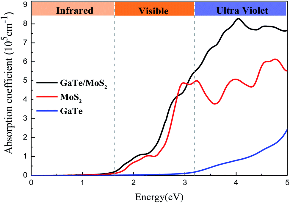 | ||
| Fig. 4 Adsorption coefficients of the GaTe monolayer, MoS2 monolayer, and GaTe/MoS2 vdWH. | ||
Recently, many studies have shown that applying external strain is an effective approach to tune electronic properties of 2D materials.17 In order to further understand the influence of the mechanical strain (compressive and tensile strain) of the vdWH on the electronic properties, we apply biaxial strain (−9% ≤ ε ≤ 9%) to the system. By changing the lattice parameters, the in-plane biaxial strain on the GaTe/MoS2 vdWH is simulated and calculated with the formula ε = [(a − a0)/a0] × 100%, where a0 and a represent the lattice parameters of unstrained and strained of the vdWH, respectively. The variation of the band gaps of the monolayers and GaTe/MoS2 vdWH with different strains is shown in Fig. 5 and in Fig. S2 in the ESI.† It is clearly that for the GaTe/MoS2 vdWH, when the compressive strain changes from −9% to −2%, the band gap monotonically increases; when the strain changes from −2% to 9%, the band gap monotonically decreases. And for tensile and compressive strains in excess of 9%, the GaTe/MoS2 vdWH has undergone a semiconductor-to-metal transition, which means that the vdWH has adjustable conductive and transmission properties. Additionally, the band gap variation of GaTe monolayer and MoS2 monolayer as a function of strain exhibits a similar trend compared with those in the GaTe/MoS2 vdWH.
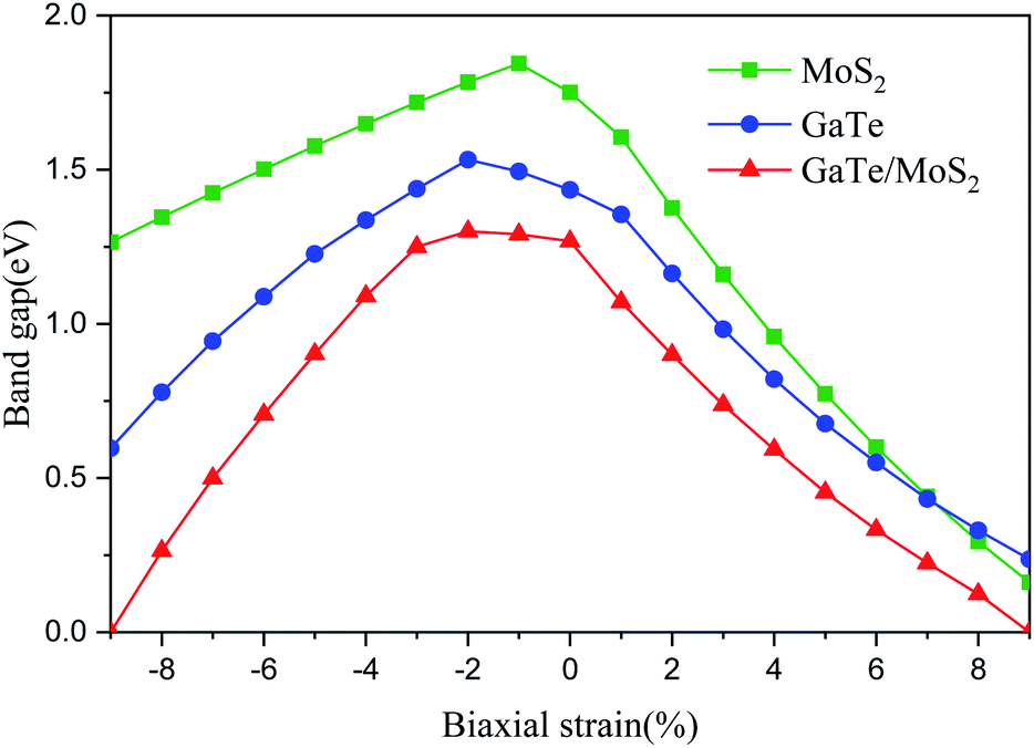 | ||
| Fig. 5 Effects of strain on the band gaps of GaTe and MoS2 monolayers and the GaTe/MoS2 vdWH. Here, positive strain and negative strain represent tensile and compression, respectively. | ||
For optical properties, a relative change occurs after applying the biaxial strain. From Fig. 6(a), we can see that the optical absorption coefficients in visible region increase as the tensile strain increases. That is to say, the optical absorption in low energy region widens, especially in the visible regions. In the visible spectrum, the results show that the tensile strain causes a red shift of the spectrum. It is well known that when the optical band gap is small, less energy can be used to excite photoelectrons. In Fig. 6(a), the optical band gap of the GaTe/MoS2 vdWH is significantly reduced after the strain is applied, and the light absorption is enhanced in the visible light region. This shows that we can use lower energy to excite the photoelectrons in the heterostructure compared to the non-stressed. And similarly, in Fig. 6(b), it can be seen that the compressive strains significantly enhance light absorption in the ultraviolet region. Thus, the tensile and compressive strain have opposite effects on the optical absorption coefficient in the ultraviolet region. The tensile strains increase the optical absorption coefficients in infrared and visible regions, however, the compressive strain increase the optical absorption coefficients in ultraviolet region. Overall, these results indicate that the optical properties of the vdWH can be effectively tuned by biaxial strain.
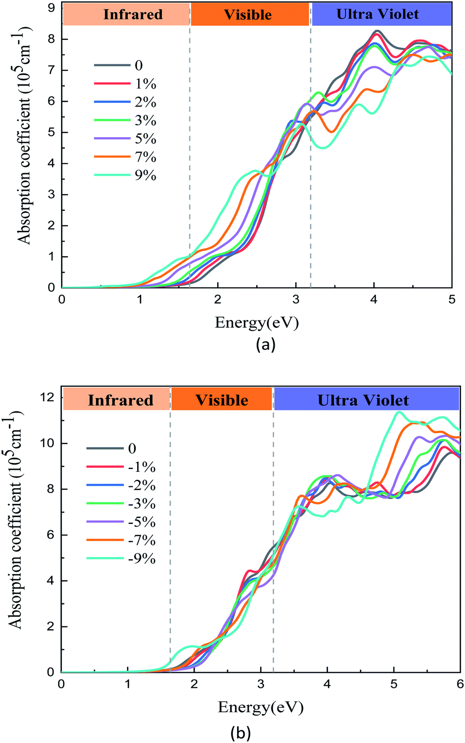 | ||
| Fig. 6 The optical adsorption spectrum of GaTe/MoS2 vdWH under (a) tensile and (b) compressive strains. | ||
4. Conclusions
In summary, we have investigated the structural, electronic, and optical properties of GaTe/MoS2 vdWH through first principles calculations. Our results show that such GaTe/MoS2 vdWH is characterized by the weak vdW interactions between the GaTe and MoS2 monolayers. GaTe/MoS2 vdWH exhibits an indirect band gap semiconductor with type-II band alignment, in which the electrostatic potential and charge difference also indicate the charge transfer from MoS2 layer to GaTe layer. Simultaneously, the GaTe/MoS2 vdWH shows enhanced optical absorption properties in the visible light region and the near infrared and UV regions compared with those in the monolayers. In addition, the band gaps and optical properties of the vdWH can be monotonically adjusted through reasonable strains, which indicates that its application prospects in electronic devices exceed other current 2D materials. In particular, large normal strains can make the system change from semiconductor to metal. Also, for optical properties, tensile strain increases the light absorption coefficient in the infrared and visible light regions, while compressive strain increases the light absorption coefficient in the ultraviolet region. These characteristics, tunable electronic structure and optical properties in GaTe/MoS2 vdWH bring new opportunities for basic research and applications of high-performance nanoelectronic and optoelectronic devices.Conflicts of interest
There are no conflicts to declare.Acknowledgements
The authors would like to acknowledge the financial support from the National Natural Science Foundation of China (Grant No. 11674197 and 11974215) and the Natural Science Foundation of Shandong Province (Grant No. ZR2018MA042). Thanks to the supporting of Taishan Scholar Project of Shandong Province.References
- K. S. Novoselov, A. K. Geim, S. V. Morozov, D. Jiang, Y. Zhang, S. V. Dubonos, I. V. Grigorieva and A. A. Firsov, Science, 2004, 306, 666–669 CrossRef CAS PubMed.
- M. Chhowalla, H. S. Shin, G. Eda, L. J. Li, K. P. Loh and H. Zhang, Nat. Chem., 2013, 5, 263–275 CrossRef PubMed.
- M. Bernardi, M. Palummo and J. C. Grossman, Nano Lett., 2013, 13, 3664–3670 CrossRef CAS.
- J. Wang, H. B. Shu, P. Liang, N. Wang, D. Cao and X. S. Chen, J. Phys. Chem. C, 2019, 123, 3861–3867 CrossRef CAS.
- F. F. Zhu, W. J. Chen, Y. Xu, C. L. Gao, D. D. Guan, C. H. Liu, D. Qian, S. C. Zhang and J. F. Jia, Nat. Mater., 2015, 14, 1020–1025 CrossRef CAS PubMed.
- S. Balendhran, S. Walia, H. Nili, S. Sriram and M. Bhaskaran, Small, 2015, 11, 640–652 CrossRef CAS PubMed.
- B. Qiu, X. W. Zhao, G. C. Hu, W. W. Yue, X. B. Yuan and J. F. Ren, Phys. E, 2020, 116, 113729 CrossRef CAS.
- C. H. Lee, G. H. Lee, A. M. Van Der Zande, W. C. Chen, Y. L. Li, M. Y. Han, X. Cui, G. Arefe, C. Nuckolls, T. F. Heinz, J. Guo, J. Hone and P. Kim, Nat. Nanotechnol., 2014, 9, 676–681 CrossRef CAS.
- K. S. Novoselov, A. Mishchenko, A. Carvalho and A. H. Castro Neto, Science, 2016, 353, 9439 CrossRef.
- F. Withers, O. Del Pozo-Zamudio, A. Mishchenko, A. P. Rooney, A. Gholinia, K. Watanabe, T. Taniguchi, S. J. Haigh, A. K. Geim, A. I. Tartakovskii and K. S. Novoselov, Nat. Mater., 2015, 14, 301–306 CrossRef CAS PubMed.
- X. W. Zhao, Z. Yang, J. T. Guo, G. C. Hu, W. W. Yue, X. B. Yuan and J. F. Ren, Sci. Rep., 2020, 10, 4028 CrossRef CAS PubMed.
- B. Qiu, X. W. Zhao, Y. Li, R. D. Liang, G. C. Hu, W. W. Yue, X. B. Yuan and J. F. Ren, Phys. Lett. A, 2020, 384, 126663 CrossRef CAS.
- Y. C. Lin, R. K. Ghosh, R. Addou, N. Lu, S. M. Eichfeld, H. Zhu, M. Y. Li, X. Peng, M. J. Kim, L. J. Li, R. M. Wallance, S. Datta and J. A. Robinson, Nat. Commun., 2015, 6, 7311 CrossRef CAS PubMed.
- M. Massicotte, P. Schmidt, F. Vialla, K. G. Schädler, A. Reserbat-Plantey, K. Watanabe, T. Taniguchi, K. J. Tielrooij and F. H. L. Koppens, Nat. Nanotechnol., 2016, 11, 42–46 CrossRef CAS PubMed.
- X. Li, M. W. Lin, J. Lin, B. Huang, A. A. Puretzky, C. Ma, K. Wang, W. Zhou, S. T. Pantelides, M. Chi, I. Kravchenko, J. Fowlkes, C. M. Rouleau, D. B. Geohegan and K. Xiao, Sci. Adv., 2016, 2, 1501882 CrossRef PubMed.
- J. Zhang, X. Y. Lang, Y. F. Zhu and Q. Jiang, Phys. Chem. Chem. Phys., 2018, 20, 17574–17582 RSC.
- C. Lei, Y. Ma, X. Xu, T. Zhang, B. Huang and Y. Dai, J. Phys. Chem. C, 2019, 123, 23089–23095 CrossRef CAS.
- M. W. Lin, L. Liu, Q. Lan, X. Tan, K. S. Dhindsa, P. Zeng, V. M. Naik, M. M. C. Cheng and Z. Zhou, J. Phys. D: Appl. Phys., 2012, 45, 345102 CrossRef.
- Q. Li, Q. Zhou, L. Shi, Q. Chen, J. Wang and A. Huang, J. Mater. Chem. A., 2019, 7, 4291–4312 RSC.
- S. Demirci, N. Avazlı, E. Durgun and S. Cahangirov, Phys. Rev. B, 2017, 95, 115409 CrossRef.
- W. Huang, L. Gan, H. Li, Y. Ma and T. Zhai, CrystEngComm, 2016, 18, 3968–3984 RSC.
- Y. Guo, S. Zhou, Y. Bai and J. Zhao, ACS Appl. Mater. Interfaces, 2017, 9, 12013–12020 CrossRef CAS PubMed.
- A. Huang, W. Shi and Z. Wang, J. Phys. Chem. C, 2019, 123, 11388–11396 CrossRef CAS.
- X. Yuan, L. Tang, S. Liu, P. Wang, Z. Chen, C. Zhang, Y. Liu, W. Wang, Y. Zou, C. Liu, N. Guo, J. Zou, P. Zhou, W. Hu and F. Xiu, Nano Lett., 2015, 15, 3571–3577 CrossRef CAS PubMed.
- F. Liu, H. Shimotani, H. Shang, T. Kanagasekaran, V. Zólyomi, N. Drummond, V. I. Fal'ko and K. Tanigaki, ACS Nano, 2014, 8, 752–760 CrossRef CAS PubMed.
- B. Chitara and A. Ya'akobovitz, Nanoscale, 2018, 10, 13022–13027 RSC.
- F. Wang, Z. Wang, K. Xu, F. Wang, Q. Wang, Y. Huang, L. Yin and J. He, Nano Lett., 2015, 15, 7558–7566 CrossRef CAS PubMed.
- G. Kresse and J. Furthmüller, Phys. Rev. B: Condens. Matter Mater. Phys., 1996, 54, 11169 CrossRef CAS PubMed.
- G. Kresse and D. Joubert, Phys. Rev. B: Condens. Matter Mater. Phys., 1999, 59, 1758 CrossRef CAS.
- P. E. Blöchl, Phys. Rev. B: Condens. Matter Mater. Phys., 1994, 50, 17953 CrossRef PubMed.
- J. P. Perdew, K. Burke and M. Ernzerhof, Phys. Rev. Lett., 1996, 77, 3865 CrossRef CAS PubMed.
- S. Grimme, J. Comput. Chem., 2006, 27, 1787–1799 CrossRef CAS PubMed.
- H. J. Monkhorst and J. D. Pack, Phys. Rev. B: Solid State, 1976, 13, 5188 CrossRef.
- J. Wang, H. B. Shu, T. F. Zhao, P. Liang, N. Wang, D. Cao and X. S. Chen, Phys. Chem. Chem. Phys., 2018, 20, 18571–18578 RSC.
- F. A. Rasmussen and K. S. Thygesen, J. Phys. Chem. C, 2015, 119, 13169–13183 CrossRef CAS.
- M. Gajdoš, K. Hummer, G. Kresse, J. Furthmüller and F. Bechstedt, Phys. Rev. B: Condens. Matter Mater. Phys., 2006, 73, 045112 CrossRef.
- T. Eberlein, U. Bangert, R. R. Nair, R. Jones, M. Gass, A. L. Bleloch, K. S. Novoselov, A. Geim and P. R. Briddon, Phys. Rev. B: Condens. Matter Mater. Phys., 2008, 77, 233406 CrossRef.
- B. Luo, X. Wang, E. Tian, G. Li and L. Li, J. Mater. Chem. C, 2015, 3, 8625–8633 RSC.
Footnote |
| † Electronic supplementary information (ESI) available. See DOI: 10.1039/d0ra04643d |
| This journal is © The Royal Society of Chemistry 2020 |