DOI:
10.1039/D0RA04319B
(Paper)
RSC Adv., 2020,
10, 25143-25154
Influence of trivalent Cr ion substitution on the physicochemical, optical, electrical, and dielectric properties of sprayed NiFe2O4 spinel-magnetic thin films
Received
14th May 2020
, Accepted 15th June 2020
First published on 2nd July 2020
Abstract
In this study, we mainly investigated the effects of trivalent Cr ion substitution on the properties of nickel ferrite (NCF) spinel-thin films. The as-prepared spinel thin films were characterized by thermogravimetry-differential thermal analysis (TGA-DTA) to comprehensively examine their phase transition. X-ray diffraction (XRD) analysis revealed that the prepared films have a single-phase face-centered cubic crystal structure. A Raman study confirmed the arrangement of the inverse-cubic spinel structure of these spinel-thin films. Field-emission scanning electron microscopy (FE-SEM) images verified the slight agglomeration of particles. Similarly, transmission electron microscopy (TEM) images together with selected area electron diffraction (SAED) patterns supported the XRD results. PL spectra showed enhanced near band emission (NBE) intensity due to the passivation of oxygen vacancies by Cr3+ substitution. The DC electrical resistivity (ρ) increases from 1.4 × 10⁻⁶ Ω cm to 4.42 × 10⁻⁶ Ω cm at room temperature. Dielectric parameters were studied as a function of frequency in the range of 1–10 MHz at 300 K, and these parameters decreased with the increasing Cr3+ ion concentration in the spinel-thin films. The obtained results indicate the applicability of the fabricated thin films in high-frequency electronic devices.
1. Introduction
Recently, nanoscale spinel structured ferrites have attracted the interest of scientists and technologists due to their significant physicochemical properties and broad applicability in magnetic storage systems,1 high-frequency devices,2 magnetic switches,1 nano-photo-catalysis,3,4 nano-fluid systems,5 spintronic devices,6 ferrofluids,7 bio-separations,8 drug delivery,9 and magnetic hyperthermia.10,11 At the nanoscale, ferrites with higher surface areas possess prominent magnetic and electrical properties over their bulk forms.12 Nano-spinel ferrites have the typical formula of ‘AB2O4’, where the ‘A2+’ and ‘B3+’ ions respectively possess ‘tetra (–A–)’ and ‘octa [–B–]’ sites.13–15 The oxygen ions form a cubic structure with the iron ions situated at two distinct interstices between them: tetra (A) and octa [B] sites. Among the various types of ferrites, spinel ferrites represent a significant set of dedicated magnetic materials and have been broadly applied in computer memories, rationale gadgets, transformer-cores, recording plates, radio wire poles, stacking loops, bio-applications, and microwave gadgets.16–19 Ferrite thin films are a potential candidates for numerous electrical and electronic devices. Ferrite thin films are appealing materials owing to their fixed magneto-electric properties and high synthetic dependability, which are valuable for some applications, for example, magnetic recording media, magnetic and gas sensors, and microwave gadgets.20–23 Ferrite thin films are being broadly considered by numerous scientists to examine their deposition and growth mechanism and structural, optical, magnetic, and electrical properties.
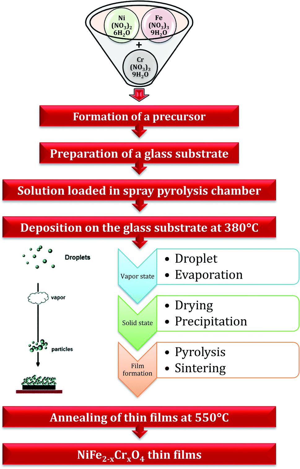
Among all the spinel ferrites, nickel ferrite (NiFe2O4) is a high-quality candidate for technological applications, and its unique macroporous films can open up new opportunities for a wide range of advanced applications.24,25 Nickel ferrites in a thin-film form are of prime interest due to their superior magnetic, electrical, and dielectric properties with greater chemical steadiness and lower magnetic loss factor at high frequencies.26 They have an irregular spinel structure and are malleable magnetic materials with a spinel-inverse structure.27 Nickel-ferrite thin films in the nanocrystalline form are applicable for use in memory gadgets,28 sensors,29 catalysis, and diverse applications.30 Gunjakar et al.31 have prepared the ferrite thin films of nickel onto a glass substrate utilizing a synthetic strategy. The XRD patterns of these films demonstrated the formation of a nano-sheet along the (311) plane. Microstructural investigation of these thin films indicated a sheet-like structure with an average thickness of 30 nm. To obtain precision in the performance of thin film-based gadgets, control over the film properties is essential. Sredojevic et al.32 have conducted initial and other examinations on Ni–Fe thin films by a spin-coating strategy. Pawar et al.33 have investigated the impact of Cr3+ substitution on the structural and other properties of NiFe2O4 films via physical techniques. The XPS results proposed that Ni2+ and Fe3+ particles exist in tetra sites just as in octa sites, and the immersion charge radically drops when compared with that for the reverse spinel structure. Along these lines, a few endeavors have been made by researchers to deposit ferrite thin films by various procedures. The physical methods comprise pulsed laser deposition and RF sputtering,34,35 whereas the chemical techniques include spray pyrolysis, chemical vapor deposition, and chemical bath deposition.23,36 However, physical methods, such as pulsed laser deposition, have the merit of providing control over the film development and thereby over each parameter of the thin film. Similarly, wet chemical techniques are being significantly considered by numerous analysts for the preparation of thin films because they are facile and economic and require low temperatures. Many wet chemical methods, specifically substance spray pyrolysis, sol–gel process, spin coating, and so forth, are generally used for the deposition of the thin films of spinel ferrites.37–40 Among the few wet chemical techniques, spray pyrolysis has some merits because of its simple experimental setup and cost-effectiveness. This technique is generally applicable for the generation of ferrite thin films with a more significant surface area with consistant thin film layer formation. Spray pyrolysis is a fundamental chemical deposition technique in which fine droplets of the solution containing stoichiometric metal ions is sprayed on preheated substrates, which is glass in most of the cases.41 Thermal decomposition takes place on the glass substrates, bringing about an thin film layer formation in thin film.
As indicated by a literature overview, nickel ferrite is an inverse spinel ferrite in which nickel ions are present at octahedral sites. Moreover, Fe3+ ions are similarly disseminated amongst the tetrahedral (A) and octahedral [B] sites.23 The presence of non-magnetic particles, such as Cr3+, instead of magnetic iron ions can offer fascinating changes in electrical properties as like as magnetic properties. In the literature, many studies have been reported on the fabrication and investigation of the magneto-electric properties of nickel ferrite in the thin film form. However, to the best of our knowledge, to date, no study has been reported on Cr3+ impurity-substituted nickel ferrite thin films. Herein, we report Cr3+-substituted nickel ferrite thin films, with the matrix equation NiFe2−xCrxO4 (for x = 0.0–1.0 in the step of 0.2), deposited on preheated (380 °C) silica glass substrates by the spray pyrolysis method followed by annealing at 550 °C for 2.5 h. Furthermore, the annealed films were characterized by standard techniques to determine the impact of Cr3+ ion substitution on the structural, thermal, morphological, dielectric, electrical, and optical properties of these nickel ferrite thin films.
2. Experimental
A spray pyrolysis strategy was employed to fabricate the thin films of NiFe2−xCrxO4 (for x = 0.0–1.0 in the venture of 0.2) (NCF) on silica glass plates (cleaned by an ultrasonication process). We have comprehensively reported the stepwise deposition process in a previous study.42 A schematic of the deposition of the NCF thin films on silica glass plates via the spray pyrolysis technique is depicted in Fig. 1. Thermogravimetric and differential thermal analysis (TGA-DTA) was employed to elucidate the thermal behavior of the typical as-deposited thin-film samples. The structural parameters of all the thin films were investigated by an X-ray diffractometer using ‘Cu-Kα’ rays in the 2θ range of 20–80°. Raman spectra were recorded at 300 K by a ‘Micro-Raman Spectrometer’. The film thickness was estimated by a surface profiler. The surface morphology of the thin films was studied using field-emission scanning electron microscopy (FE-SEM) and transmission electron microscopy (TEM) accompanied by selected area electron diffraction (SAED). Elemental analysis was conducted by energy dispersive X-ray (EDAX) analysis. Herein, the four-probe technique was employed to obtain the DCR plot as a function of temperature in the range between 303 and 723 K. A dielectric study was performed to examine the dielectric parameters at 300 K as a function of frequency in the range from 1 to 1 MHz.
 |
| | Fig. 1 Schematic of the deposition process of the NCF thin films. | |
3. Results and discussion
3.1 Thermal analysis
The TGA-DTA plot for the growth procedure of the as-deposited thin-film samples of NiFe2O4 (continuous line) and NiFe1.2Cr0.8O4 (dashed line) in the temperature range from 20 to 800 °C is shown in Fig. 2. The TGA curve starts to diminish from room temperature to 470 °C, which demonstrates a solitary real weight reduction of ∼10%, and the concurrent DTA curve demonstrates the exothermic peak at 430 °C. An exothermic peak appears at 430 °C, corresponds to the weight reduction in the temperature range of 200 to 500 °C, and a little exothermic peak appears at 195 °C.43
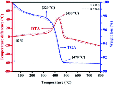 |
| | Fig. 2 The TGA-DTA curve of the as-prepared NiFe2O4 (continuous line) and NiFe1.2Cr0.8O4 (dashed line) thin films. | |
In the TGA curve, a decrement in the weight is observed at 320 °C because of water loss and a gradual crystallization process occurring from 470 to 800 °C in the thin film sample. The maximum weight reduction in the temperature range from 470 to 800 °C affirms the development of a crystalline and spinel structure. The most extreme weight reduction at 320–460 °C is due to the removal of water, contaminations, and nitrates and decay of the original mixes.44,45 At temperatures higher than 470 °C, the weight reduction remains constant. The same trend was observed for the NiFe1.2Cr0.8O4 sample designated by a dashed line (Fig. 2). The TGA curve demonstrates that the rate of weight loss is nearly constant above 470 °C. Therefore, the annealing temperature of 550 °C was used for all the resultant NCF samples.
3.2 X-ray diffraction
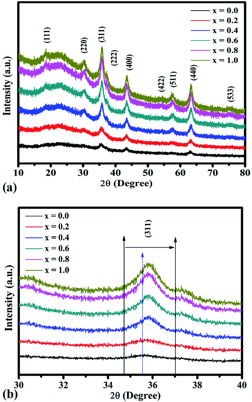
The XRD patterns of the NCF thin-film samples are depicted in Fig. 3(a). All the obtained XRD patterns demonstrate diffraction peaks corresponding to those of a cubic spinel structure, and a closer assessment of the XRD patterns of the samples demonstrates the absence of peaks related to other unwanted phases. Upon careful observation of the XRD patterns, the presence of small intensity peaks was noticed, which might be because of the small thickness of the prepared thin films. The diffraction peaks corresponded to the (111), (220), (311), (222), (400), (422), (511), (440), and (533) reflections of the mixed spinel-ferrites with cubic structure affirms high crystallinity of the films. The Debye–Scherrer formula was used to determine the average crystallite size (D) of the prepared samples:46| |
 | (1) |
where λ is the X-ray wavelength and β is the line width at half the line intensity obtained by taking into account the instrumental broadening. The average crystallite sizes of the prepared thin films were in the range of 23.56–45.15 nm. In fact, the crystallite sizes were decreased, as indicated by the induced strain and broadening peaks obtained with the substitution of the Cr3+ ion. The lattice parameter was calculated using the following relation.47| |
 | (2) |
where θ is the Bragg's angle and (hkl) are the Miller indices of the planes. The peak (311) moved towards higher 2θ angles, as shown in Fig. 3(b). The concentration of the Cr3+ ions increases, affirming a decrease in the lattice constant from 8.2780 to 8.3273 Å. The reduction in the lattice parameter values is because of the lower ionic radius of the Cr3+ ions (0.63 Å) when compared with that of the Fe3+ ions (0.67 Å). The X-ray density of the NCF thin films has been determined from the molecular weight and unit cell volume using the following relation:48| |
 | (3) |
where NA is the Avogadro's number and a is the lattice parameter of the NCF samples. The values of the structural parameters, such as lattice constant and X-ray density, are presented in Table 1. The X-ray density decreases with the increasing substitution of the Cr3+ ions; this is due to the substitution of the Cr3+ ions with a smaller molar mass (51.996 g mol−1) for the Fe3+ ions with a larger molar mass (55.845 g mol−1).
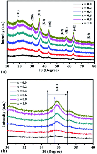 |
| | Fig. 3 (a) X-ray diffraction patterns of the NiFe2−xCrxO4 thin films. (b) Shifting of the most intense (311) peak of the NiFe2−xCrxO4 thin films. | |
Table 1 Lattice constant (a), X-ray density (dx), and average crystallite size (D) of the NiFe2−xCrxO4 thin films
| Composition x |
‘a’ (Å), (±0.10) |
‘dx’ (gm cm−3), (±0.01) |
‘D’ (nm), (±2.0) |
| 0.0 |
8.3273 |
5.392 |
45.15 |
| 0.2 |
8.3233 |
4.096 |
35.38 |
| 0.4 |
8.3201 |
4.082 |
33.75 |
| 0.6 |
8.2990 |
4.096 |
29.34 |
| 0.8 |
8.2886 |
4.093 |
24.61 |
| 1.0 |
8.2780 |
4.091 |
23.56 |
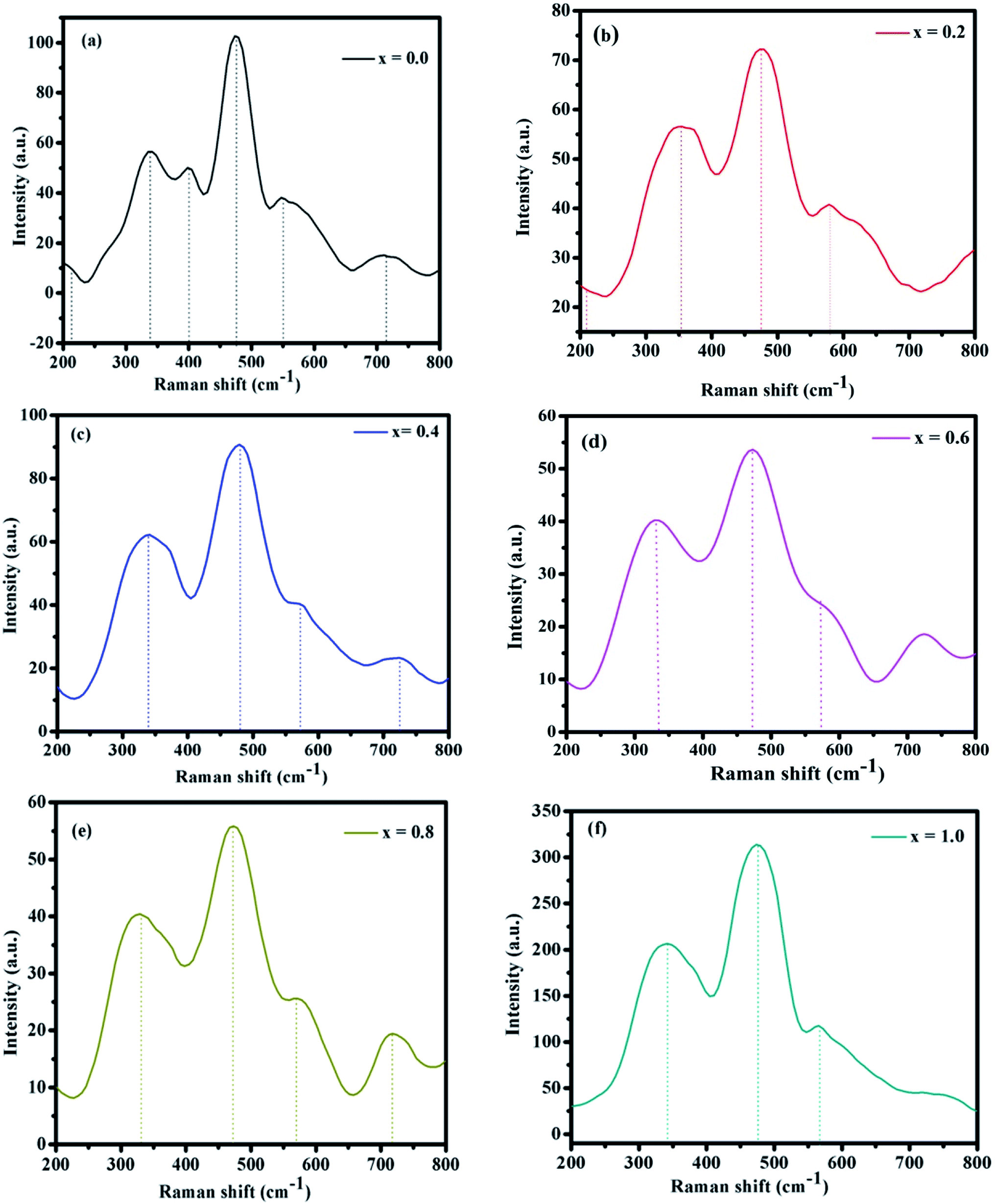
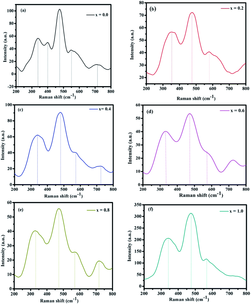
3.3 Raman spectroscopy
The room-temperature Raman spectra of the NCF samples in the wavelength range of 200–800 cm−1 are shown in Fig. 4(a–f). The Raman spectra of the ferrite with a spinel lattice structure having the space group ‘Fd![[3 with combining macron]](https://www.rsc.org/images/entities/char_0033_0304.gif) m’ specifically revealed five active Raman modes: ‘A1g + Eg + 3T2g’. The ‘A1g’ mode is generated because of the symmetric extension of the ‘O2−’ ions next to the ‘Fe–O’ and ‘Ni–O’ bonds in the ‘tetrahedral’ sites. The ‘Eg’ mode originates from the symmetric twisting of the ‘O2−’ ions as for the metal ion.49
m’ specifically revealed five active Raman modes: ‘A1g + Eg + 3T2g’. The ‘A1g’ mode is generated because of the symmetric extension of the ‘O2−’ ions next to the ‘Fe–O’ and ‘Ni–O’ bonds in the ‘tetrahedral’ sites. The ‘Eg’ mode originates from the symmetric twisting of the ‘O2−’ ions as for the metal ion.49
 |
| | Fig. 4 (a–f) Raman spectra of the NiFe2−xCrxO4 thin films. | |
In nickel ferrite, the ‘octahedral site’ is occupied by Fe3+ and Ni2+ ions, and the ‘tetrahedral site’ is accommodated by only Fe3+ ions. For all the thin-film samples, the Raman signals in the range of 540–585 cm−1 correspond to the A1g modes, which indicate extending vibration of Fe3+ or O2− ions at the octahedral site.50 The vibrational groups in the range 330–355 cm−1 corresponds to the Eg whereas, the bands in the range 470–480 cm−1 corresponds to 3T2g symmetry which is because of O2− extending at ‘octahedral’ locales. The cation relocation in spinel NiFe2O4 changes because of the shifting of the metal ions from the tetra site to the octa site.51 These site cation movements must break the extended cationic order and nearby disorder at both the tetra and the octa site sub-cross sections in the meantime. Therefore, the outcome obtained from Raman scattering demonstrates the presence of a confined disorder instigated by cationic relocation in the NiFe2O4 thin films, which is affirmed by the XRD patterns. The Raman spectra band positions for all the samples are shown in Table 2.
Table 2 Raman spectra band position of the NiFe2−xCrxO4 thin films
| Composition x |
Assigned band position (cm−1) |
| ‘A1g’ |
‘Eg’ |
‘3T2g’ |
| 0.0 |
547 |
338 |
476 |
| 0.2 |
581 |
354 |
474 |
| 0.4 |
574 |
339 |
482 |
| 0.6 |
553 |
337 |
478 |
| 0.8 |
571 |
330 |
476 |
| 1.0 |
567 |
340 |
477 |
3.4 Microstructural and compositional analysis
The FE-SEM images of the NCF thin-film samples are depicted in Fig. 5(a–d). The development of soft agglomerated particles demonstrates that the grains have a practically circular and regular shape. The magnetic dipole interaction in-between the grains loaded towards the agglomerating nature of the nano-particle with expanding Cr3+ substitution content. The Cr3+ ion substitution profoundly influences the morphology, shape, uniformity, homogeneity, and distribution of grains.52 Fig. 5(a–d) show the representative FE-SEM images of typical NiFe2−xCrxO4 (0.0, 0.4, 0.8, and 1.0) thin films. The grain size (G) values were found to diminish with an increment in the Cr3+ ion concentration in the NCF samples; this suggests the growth of the crystallites. This decrement is credited to the accommodation of Cr3+ ions in the accessible sites amid particle growth, accordingly constraining the nucleation procedure and size. All the synthesized thin-film samples exhibit granulated sand-like grains.53 The evaluated grain size is roughly in the range from 26.65 to 42.14 nm. The particles are sharp and significantly circular, demonstrating crystallinity, as affirmed by the XRD patterns. With a decrease in the film thickness, the grain size diminished and the films became compact and dense.54,55
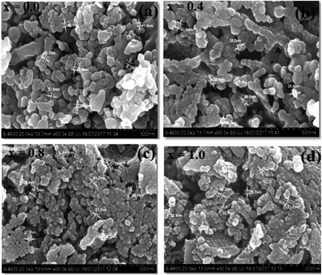 |
| | Fig. 5 (a–d) FE-SEM images of the NiFe2−xCrxO4 thin films. | |
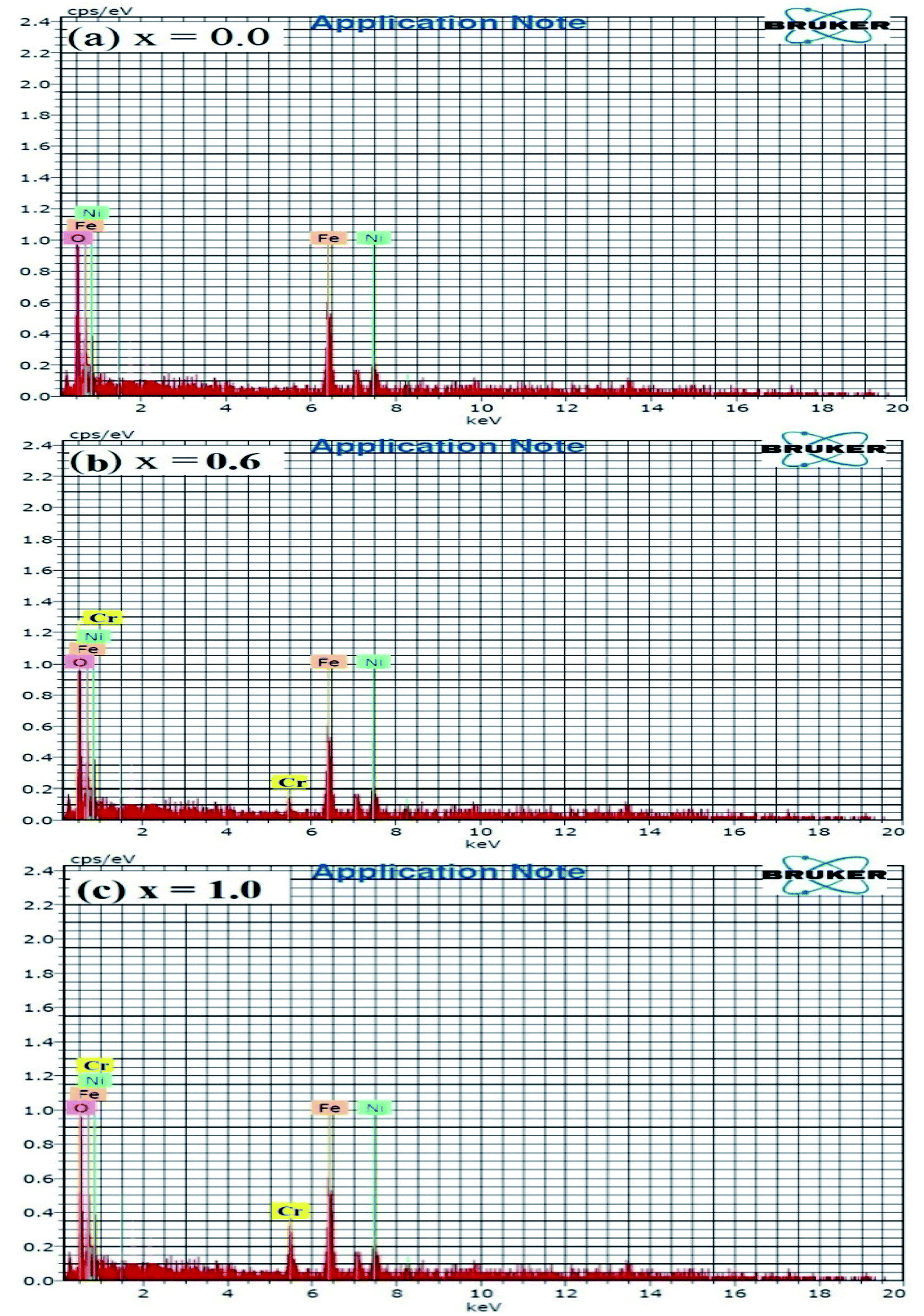
The elemental compositions of representative NCF thin films characterized by the EDAX technique are shown in Fig. 6(a–c). The EDAX technique was employed to approve the accuracy and purity of the chemical compositions. The desired peaks corresponding to Ni2+, Cr3+, Fe3+, and O2− was observed in the EDAX spectra and no impurity peak was observed. The atomic weight (%) and elemental weight (%) of the different components present in the NCF samples are in close agreement with the nominal compositions (Table 3).
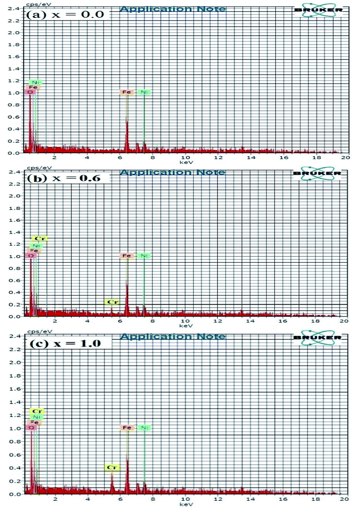 |
| | Fig. 6 (a–c) The typical EDAX spectra of the NiFe2−xCrxO4 thin films. | |
Table 3 Elemental and atomic weight percentages (%) obtained from the EDAX of the NiFe2−xCrxO4 (x = 0.0, 0.4, 0.8, and 1.0) thin films
| x |
G (nm), (±2) |
Elemental weight (%) |
Atomic weight (%) |
| Ni2+ |
Fe3+ |
Cr3+ |
O2− |
Total (%) |
Ni2+ |
Fe3+ |
Cr3+ |
O2− |
Total (%) |
| 0.0 |
42.14 |
27.3 |
34.86 |
0.00 |
37.84 |
100 |
11.94 |
19.16 |
0.00 |
68.9 |
100 |
| 0.2 |
40.13 |
27.11 |
29.14 |
5.46 |
38.29 |
100 |
11.63 |
14.68 |
7.55 |
66.14 |
100 |
| 0.4 |
34.64 |
26.58 |
22.06 |
10.33 |
41.03 |
100 |
10.93 |
11.41 |
11.08 |
66.58 |
100 |
| 0.6 |
33.12 |
28.12 |
16.45 |
18.36 |
37.07 |
100 |
10.24 |
7.9 |
17.68 |
64.18 |
100 |
| 0.8 |
28.58 |
26.85 |
9.84 |
24.46 |
38.85 |
100 |
11.91 |
3.81 |
23.23 |
61.05 |
100 |
| 1.0 |
26.65 |
28.1 |
6.12 |
22.66 |
43.12 |
100 |
11.65 |
1.92 |
21.57 |
64.86 |
100 |
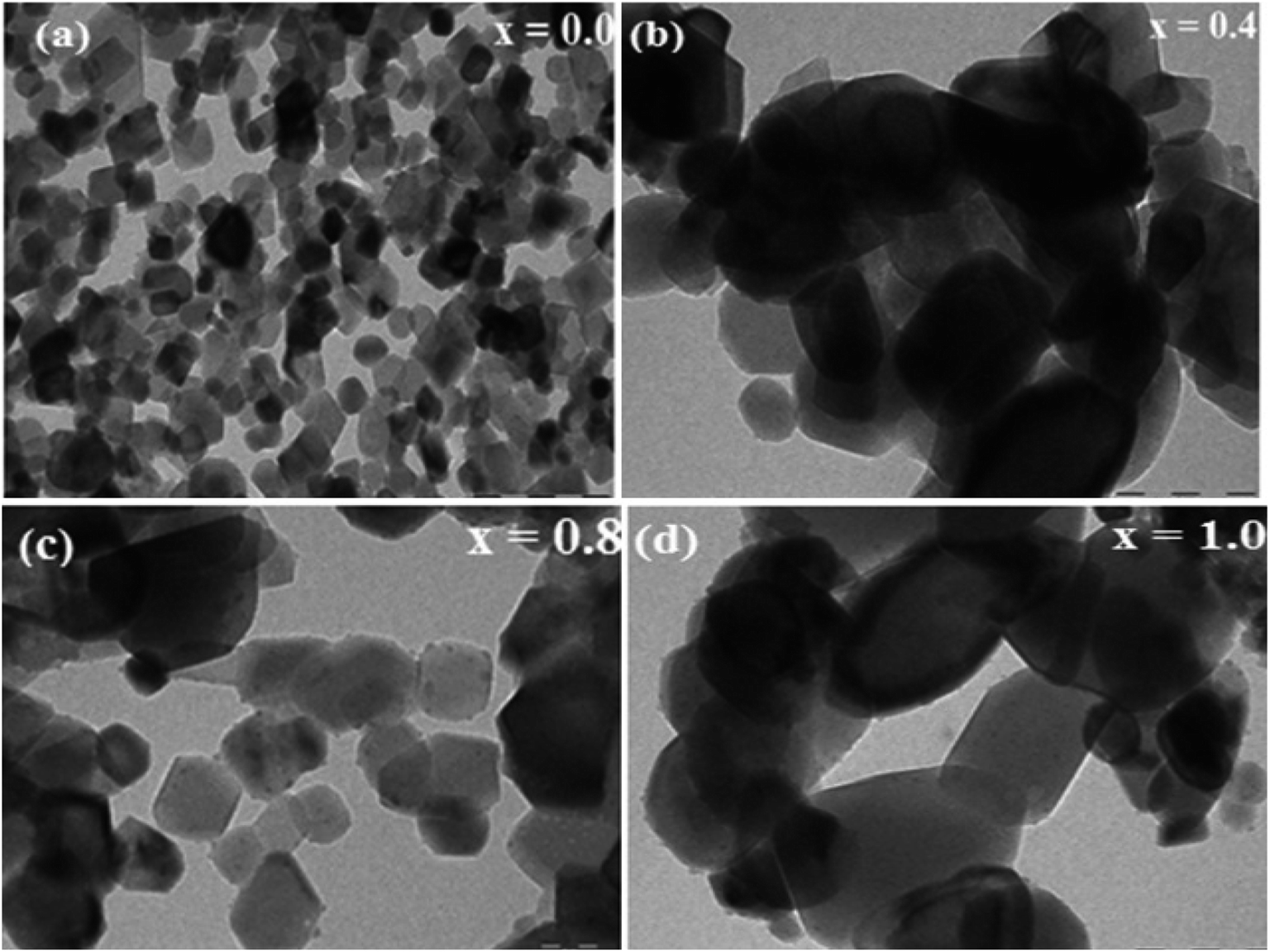
Fig. 7(a–d) show the TEM images of the typical NCF samples (x = 0.0, 0.4, 0.8, and 1.0) of the prepared thin films. The TEM images demonstrate that the nanoparticles of the film samples obtained without a surfactant have a cube-like structure and uniform particle size and surface morphology.56 The TEM images show that the significant agglomeration is because of the magnetic nature of the nanoparticles when compared with the observation made from the FE-SEM images.
 |
| | Fig. 7 (a–d) Typical TEM images of the NiFe2−xCrxO4 (0.0, 0.4, 0.8, and 1.0) thin films. | |
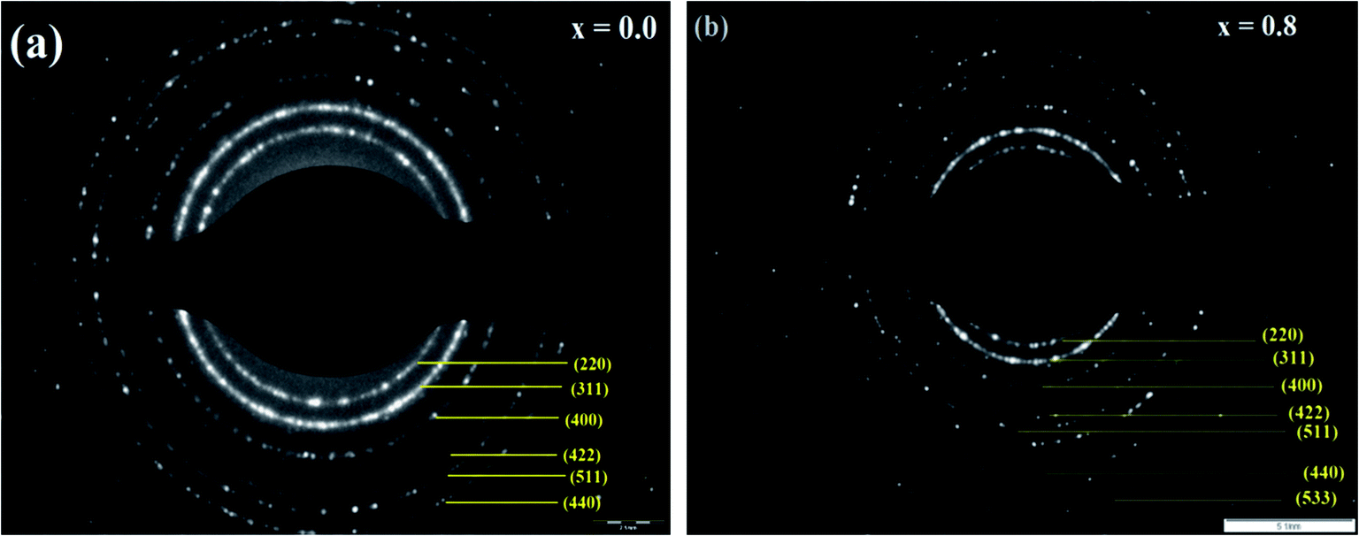
The SAED patterns of the NCF thin films (x = 0.0 and 0.8) are shown in Fig. 8(a and b). They depict well-observed diffraction rings, indicating good crystallinity and single phase of the NCF thin films. Basically, the SAED patterns showing the high intensity (311) peak represents the cubic spinel structure and d-spacing of the NCF (x = 0.0 and 0.8) thin films. Each diffraction spot ring matches with the (dhkl) spacing and indicates that the NCF samples are well-crystallized, which is consistent with the XRD outcomes.57,58
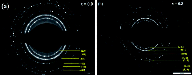 |
| | Fig. 8 (a and b) Typical SAED patterns for the NiFe2−xCrxO4 thin films with x = 0.0 and x = 0.8. | |
3.5 PL spectroscopy
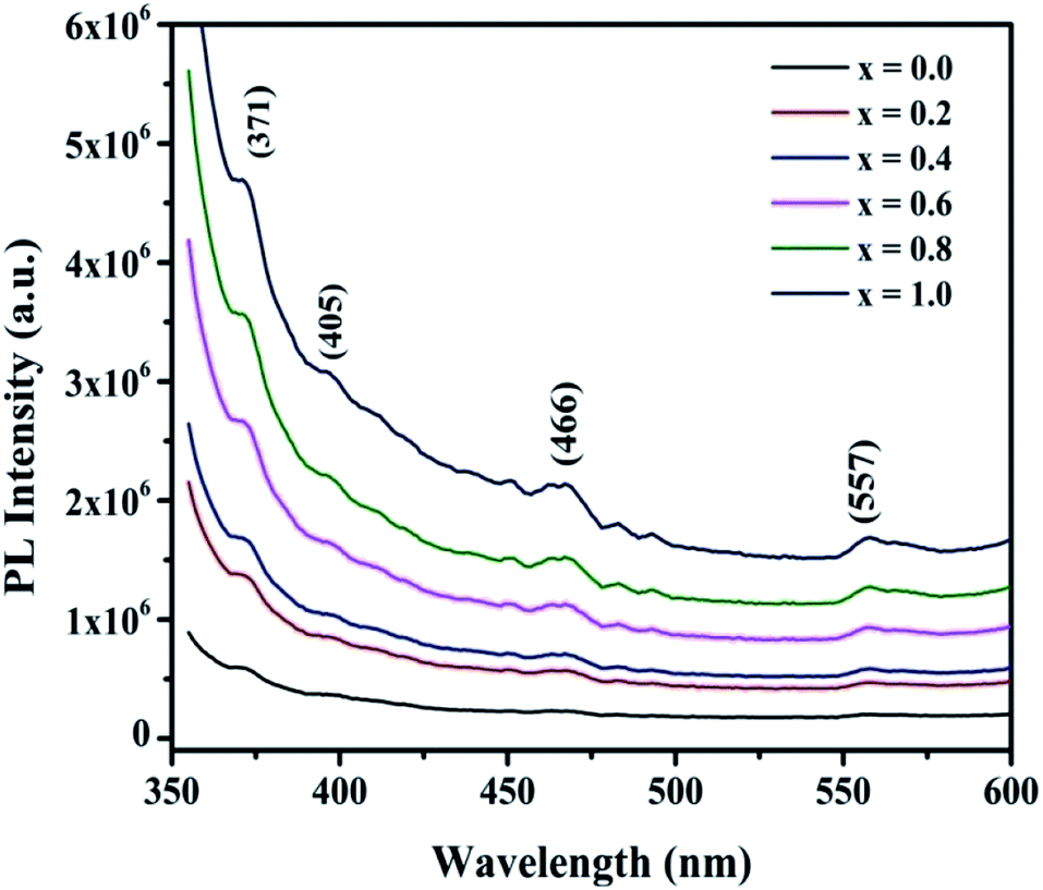
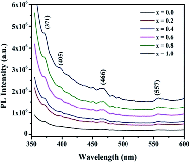
The room-temperature photoluminescence spectra of the NiFe2−xCrxO4 thin films in the range of 350–600 nm are depicted in Fig. 9. As observed, the PL spectra of the NCF samples possess a peak in the broader emission range of 350–600 nm with a band gap energy of 1.82–3.55 eV. This peak is due to the re-grouping of the charges, which happens because of lattice intrinsic defects and profound traps of the restricted surface position.59 Nickel ions are present in the ‘octal’ sites, and iron ions are present in the ‘tetra’ sites; moreover, they have the electronic arrangements 3d8 and 3d5. The PL emission spectra were acquired using 400 nm as the excitation wavelength. The peak situated between 405 and 466 nm corresponds to the near band emission (NBE), which is due to the changes from 3A2(3F) → 3T1(3P) and 3A2(3F) → 1T2(1D).60 The peaks at 371 nm and 466 nm correspond to the ‘3d5 → 3d4’conversion of Fe3+, which leads to electron excitation towards the conduction band.
 |
| | Fig. 9 Photoluminescence spectra of the NiFe2−xCrxO4 thin films. | |
The defect level emission (DLE) was obtained from the peak at 557 nm. It can be ascribed to the defects, such as oxygen vacancies, in the crystal structure and surface defects. The broader band from 540 to 560 nm is due to the transitions of the Ni2+ ions and Fe3+/Cr3+ ions.61 The intensity of the NBE increases with the increasing Cr3+ ion concentration in the NCF samples. This means that the reductions in the oxygen vacancies cause a reduction in the number of photogenerated electrons in the NCF thin films.62 The PL range demonstrates the presence of Ni2+ ions at both the octal and tetra sites, confirming the assorted spinel lattice structure of these films.
In the PL spectra, it can be clearly noticed that from x = 0.0 to x = 1.0, the PL emission intensity increases. As the sample is a deposited thin film (thickness: ∼250–300 nm), in the case of 400 nm excitation, the penetration depth of one-photon excitation is around ∼300 nm;63 hence, it can deeply penetrate the sample. Therefore, the observed PL spectra may have originated from the substrate as well, and subsequently, a wide background appears. Moreover, the PL intensity increases from x = 1.0 onwards; this means that now the excitation energy normalizes towards the bandgap of the material. In this case, under resonant pumping, there is a probability of the excitation of more molecules to the conduction band, and hence, the emission is enhanced. Under the resonant condition, all molecules are excited, and the saturation of linear absorption further results in the formation of emission.
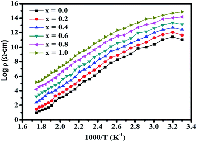
3.6 Electrical properties
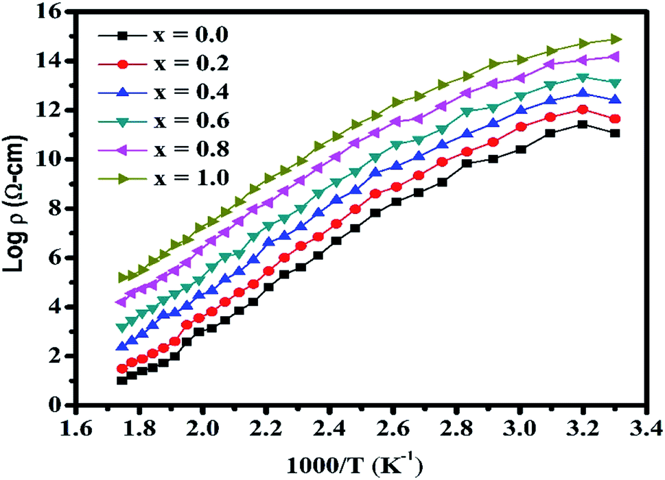
The variation in the DC electrical resistivity (DCR) versus temperature (323–723 K) for the NCF samples is shown in Fig. 10. Fig. 10 reflects that the resistivity significantly diminishes with an increment in temperature because of the hopping of electrons, which shows a semiconducting nature of the films.64 The Verwey and Bohr's system can clarify the conduction procedure in the NCF samples. During the deposition and annealing process, iron and nickel ions are generated in a small amount, and electron exchange occurs between the Fe3+ and Ni2+ ions, which can be represented as follows:| | |
Ni2+ + Fe3+ ↔ Ni3+ + Fe2+
| (4) |
 |
| | Fig. 10 DCR plots for the NiFe2−xCrxO4 thin films. | |
In the current investigation, the plot of log![[thin space (1/6-em)]](https://www.rsc.org/images/entities/char_2009.gif) ρ versus 1000 × T−1 shows the variation in slope, which makes two distinct regions namely paramagnetic region and ferromagnetic region. The variation in resistivity as a function of temperature confirms the Arrhenius relation.65 Using the DCR plots, the activation energy ΔE for each sample in the ferrimagnetic and paramagnetic locale was determined. The estimated activation energies for the all Cr3+-substituted nickel spinel ferrite samples are presented in Table 3. The estimated activation energy ‘ΔE’ values of the samples under investigation were observed to be in the range from 0.42 to 0.26 eV. In Fig. 10, it can be clearly noticed that the resistivity diminishes with the increasing temperature. This might be due to the presence of Fe3+ in the [B]-site. Notably, the conductivity of ferrite depends on the proportion of Fe3+ to Fe2+ since this proportion diminishes with the increasing concentration of Cr3+ ions; at this point, resistivity should show a constant decline with the increasing concentration of Cr3+ ions.
ρ versus 1000 × T−1 shows the variation in slope, which makes two distinct regions namely paramagnetic region and ferromagnetic region. The variation in resistivity as a function of temperature confirms the Arrhenius relation.65 Using the DCR plots, the activation energy ΔE for each sample in the ferrimagnetic and paramagnetic locale was determined. The estimated activation energies for the all Cr3+-substituted nickel spinel ferrite samples are presented in Table 3. The estimated activation energy ‘ΔE’ values of the samples under investigation were observed to be in the range from 0.42 to 0.26 eV. In Fig. 10, it can be clearly noticed that the resistivity diminishes with the increasing temperature. This might be due to the presence of Fe3+ in the [B]-site. Notably, the conductivity of ferrite depends on the proportion of Fe3+ to Fe2+ since this proportion diminishes with the increasing concentration of Cr3+ ions; at this point, resistivity should show a constant decline with the increasing concentration of Cr3+ ions.
Electrical conduction in spinel ferrite arises due to the electron bouncing in between the ion pairs of a similar element located at distinct sublattices with difference valence state. The quantity of these ion pairs relies on the sintering circumstances and degree of decrease of Fe3+ ↔ Fe2+ at a raised temperature. The proportion of Fe2+/Fe3+ at the [B]-sites controls the general resistivity in ferrite materials.66 The breaking of the DCR plots in two areas of conductivity affirms the temperature associated with the Curie temperature (Tc) of the samples. The lower temperature area underneath the Curie temperature is related to the arranged ferromagnetic area having a little ΔE, whereas the superior temperature locale over Tc corresponds to a paramagnetic area with relatively high activation energy.67,68 A sharp and huge increment in resistivity at low concentrations of the dopants is very evident, whereas the expansion is less articulated for higher concentrations. However, direct magnetic loss estimations in a wide frequency range and their complete analysis are required to thoroughly address the pertinence of Cr3+-substituted nickel ferrite materials for microwave applications (Table 4).
Table 4 DC electrical resistivity (ρ), activation energy (ΔE), and thickness (T) of the NCF thin films
| x |
ρ (Ω cm) × 106 |
ΔE (eV) |
T (nm) |
| 0.0 |
1.40 |
0.42 |
277 |
| 0.2 |
1.62 |
0.38 |
265 |
| 0.4 |
2.30 |
0.34 |
256 |
| 0.6 |
2.80 |
0.29 |
248 |
| 0.8 |
3.64 |
0.27 |
283 |
| 1.0 |
4.46 |
0.26 |
287 |
3.7 Dielectric parameter studies
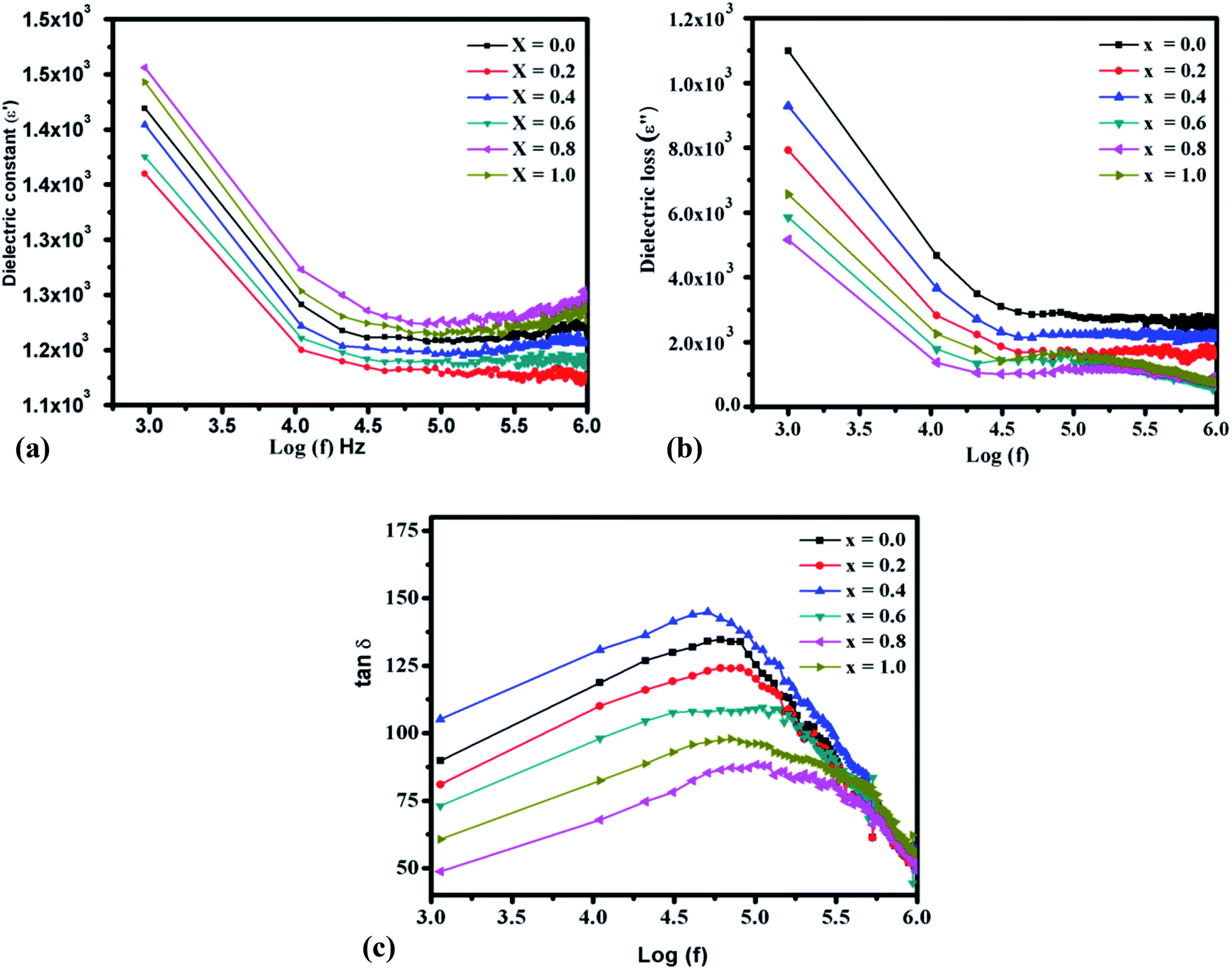
The dielectric properties of spinel ferrite thin films firmly rely upon a few variables including the deposition procedure, chemical composition, grain structure, stoichiometry, percentage porosity values, the charge of ions, grains size, and cationic dissemination among the interstitial sites. Dielectric parameters are beneficial for the absorption of electromagnetic waves.69–72 Fig. 11(a) shows the variation of the real part of the dielectric constant versus frequency for the as-prepared Cr3+-substituted nickel ferrites with various compositions. The dielectric constant (ε′) is enhanced in the lower frequency range and diminishes with the increasing frequency. There are diminishing pattern in the least value with the increasing frequency,73 which shows the typical behavior of ‘ferromagnetic’ materials. The higher dielectric constant at lower frequencies might be because of the simultaneous presence of various types of polarization contributions of space charges and further it starts to diminish with an increase in frequency.74 As per the Koop's hypothesis, the decrease in the dielectric constant with the increasing frequency is because, at higher frequencies, several factors impact the polarization to indicate change in the functional field. The dielectric constant (ε′) was determined utilizing the following formula:75| |
 | (5) |
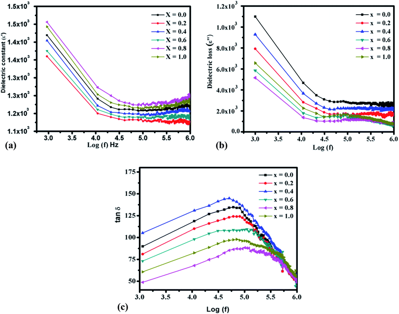 |
| | Fig. 11 (a) Variation of dielectric constant for the NiFe2−xCrxO4 thin films. (b) Variation of dielectric loss for the NiFe2−xCrxO4 thin films. Variation of the dielectric loss tangent for the NiFe2−xCrxO4 thin films. | |
The decrease in dielectric constant was observed due to the electrical polarization. The present examinations demonstrated that the dielectric constant (ε′) of the NCF samples is higher than that of the pure nickel ferrite thin film. The reason behind these variations might be the concentration of Cr3+ ions, which decreases the hopping of the electrons over grain boundries.49 The reduction in the dielectric constant was because outside a specific frequency of the externally applied field, the electronic exchange between Fe3+ ↔ Fe2+ ions does not appear. A higher value of the dielectric constant at lower frequencies is because of the inhomogeneous dielectric structure in the ferrite materials. The inhomogeneities present in the material can be oxygen vacancies, grain boundary defects, dislocations, high concentration of Fe2+ ions, and porosity. The substitution of Cr3+ in nickel ferrite increases the gathering of charges at the grain limits, and consequently, the dielectric constant decreases.76 The Cr3+ ion substitution in nickel ferrite for Fe3+ ions was effective in decreasing the dielectric loss (ε′′), as shown in Fig. 11(b). According to the free electron theory, the dielectric loss primarily originates from the conductive loss, and the tested ε′′ value will decrease with the increasing frequency.77 Fig. 11(b) also shows that the pure nickel ferrite thin-film sample possesses a significant value of the dielectric loss, which diminishes from x = 0.2 to x = 1.0 with the increasing Cr3+ substitution. This behaviour demonstrates the loss in energy at the higher frequencies and thus prepared NCF samples are promising for high-frequency electronic device applications. Fig. 11(c) demonstrates the variation of the dielectric loss tangent (tanδ) as a function of frequency estimated at 300 K. The tanδ value diminishes with the increasing frequency, which can be clarified by the ‘Koop's model’.78,79 The estimation of loss tangent depends on various factors, for instance, the presence of Fe2+ ions and homogeneity of the NCF samples, which relies upon the deposition and annealing temperatures.
4. Conclusions
Herein, the TGA-DTA data confirmed the thermal behavior of the typical thin-film samples of Ni–Cr ferrite. XRD patterns demonstrated the development of single-phase cubic structure in all the prepared samples with nanocrystalline nature. Raman spectra show tetra and octa sites in the structure of NiFe2−xCrxO4 and suggest the substitution of Cr3+ ions and displacement of Ni2+ particles to the tetrahedral site. The studies conducted by the FE-SEM technique revealed the development of grains with a spherical structure, agglomerated configuration, and grain size in the range of 26.65–42.14 nm. The results of the elemental analysis performed by EDAX are in close agreement with the projected composition obtained from the stoichiometry of the initial compositions used for the synthesis. The photoluminescence spectra revealed their combination phenomena belonging to semiconductor materials, indicating intrinsic bandgap defect states in the prepared ferrite thin films. The DC electrical resistivity decreases as the temperature increases, implying the semiconducting behavior of the fabricated NCF thin films. In addition, the DC electrical resistivity was observed to be enhanced with an increase in the Cr3+ ion substitution. All the dielectric parameters decline with an increase in frequency, corresponding to the Verwey and Bohr's model. The obtained outcomes pave the way for the applicability of the fabricated thin films in high-frequency electronic devices.
Conflicts of interest
There are no conflicts to declare.
Acknowledgements
The author ARC is very much thankful to Kavayitri Bahinabai Chaudhari, North Maharashtra University, Jalgaon, for the FE-SEM measurements and University of Mysore, Mysore, for providing the dielectric measurement facility. The author Sandeep B. Somvanshi acknowledges Department of Science and Technology (DST), Government of India, for DST-Inspire Fellowship (IF170288).
References
- W. Hu, N. Qin, G. Wu, Y. Lin, S. Li and D. Bao, J. Am. Chem. Soc., 2012, 134, 14658–14661 CrossRef CAS PubMed.
- A. Subramani, K. Kondo, M. Tada, M. Abe, M. Yoshimura and N. Matsushita, Mater. Chem. Phys., 2010, 123, 16–19 CrossRef CAS.
- S. A. Jadhav, S. B. Somvanshi, M. V. Khedkar, S. R. Patade and K. M. Jadhav, J. Mater. Sci.: Mater. Electron., 2020, 31(14), 11352–11365 CrossRef CAS.
- R. M. Borade, S. B. Somvanshi, S. B. Kale, R. P. Pawar and K. Jadhav, Mater. Res. Express, 2020, 7, 016116 CrossRef CAS.
- P. B. Kharat, S. More, S. B. Somvanshi and K. Jadhav, J. Mater. Sci.: Mater. Electron., 2019, 30, 6564–6574 CrossRef CAS.
- U. Lüders, A. Barthelemy, M. Bibes, K. Bouzehouane, S. Fusil, E. Jacquet, J. P. Contour, J. F. Bobo, J. Fontcuberta and A. Fert, Adv. Mater., 2006, 18, 1733–1736 CrossRef.
- P. B. Kharat, S. B. Somvanshi, J. S. Kounsalye, S. S. Deshmukh, P. P. Khirade and K. M. Jadhav, AIP Conf. Proc., 2018, 1942, 050044 CrossRef.
- S. B. Somvanshi, P. B. Kharat, T. S. Saraf, S. B. Somwanshi, S. B. Shejul and K. M. Jadhav, Mater. Res. Innovations, 2020, 1–6, DOI:10.1080/14328917.2020.1769350.
- S. B. Kale, S. B. Somvanshi, M. N. Sarnaik, S. D. More, S. J. Shukla and K. M. Jadhav, AIP Conf. Proc., 2018, 1953, 030193 CrossRef.
- S. R. Patade, D. D. Andhare, S. B. Somvanshi, P. B. Kharat, S. D. More and K. M. Jadhav, Nanomater. Energy, 2020, 1–6 Search PubMed.
- S. B. Somvanshi, S. R. Patade, D. D. Andhare, S. A. Jadhav, M. V. Khedkar, P. B. Kharat, P. P. Khirade and K. M. Jadhav, J. Alloys Compd., 2020, 835, 155422 CrossRef CAS.
- Z. Gao, B. Xu, M. Ma, A. Feng, Y. Zhang, X. Liu, Z. Jia and G. Wu, Composites, Part B, 2019, 179, 107417 CrossRef CAS.
- Z. Jiao, M. Wu, J. Gu and Z. Qin, IEEE Sens. J., 2003, 3, 435–438 CrossRef CAS.
- R. R. Chilwar, A. R. Chavan, M. Babrekar and K. Jadhav, Phys. B, 2019, 566, 43–49 CrossRef CAS.
- S. B. Somvanshi, S. A. Jadhav, M. V. Khedkar, P. B. Kharat, S. D. More and K. M. Jadhav, Ceram. Int., 2020, 46, 13170–13179 CrossRef CAS.
- S. Patange, S. E. Shirsath, B. Toksha, S. S. Jadhav and K. Jadhav, J. Appl. Phys., 2009, 106, 023914 CrossRef.
- R. Zhang, M. Liu, L. Lu, S.-B. Mi and H. Wang, CrystEngComm, 2015, 17, 8256–8263 RSC.
- X. Chen, X. Zhu, W. Xiao, G. Liu, Y. P. Feng, J. Ding and R.-W. Li, ACS Nano, 2015, 9, 4210–4218 CrossRef CAS PubMed.
- S. B. Somvanshi, R. V. Kumar, J. S. Kounsalye, T. S. Saraf and K. M. Jadhav, AIP Conf. Proc., 2019, 2115, 030522 CrossRef.
- D. S. Mathew and R.-S. Juang, Chem. Eng. J., 2007, 129, 51–65 CrossRef CAS.
- G. Hu, J. Choi, C. Eom, V. Harris and Y. Suzuki, Phys. Rev. B: Condens. Matter Mater. Phys., 2000, 62, R779 CrossRef CAS.
- Y.-N. NuLi and Q.-Z. Qin, J. Power Sources, 2005, 142, 292–297 CrossRef CAS.
- A. Abou-Hassan, S. Neveu, V. Dupuis and V. Cabuil, RSC Adv., 2012, 2, 11263–11266 RSC.
- G. Fan, X. Xiang, J. Fan and F. Li, J. Mater. Chem., 2010, 20, 7378–7385 RSC.
- M. Babrekar and K. Jadhav, Int. Res. J. Sci. Eng., 2017, 73–76 Search PubMed.
- H. J. Kardile, S. B. Somvanshi, A. R. Chavan, A. A. Pandit and K. M. Jadhav, Optik, 2020, 207, 164462 CrossRef CAS.
- V. Bharati, S. B. Somvanshi, A. V. Humbe, V. Murumkar, V. Sondur and K. Jadhav, J. Alloys Compd., 2020, 821, 153501 CrossRef CAS.
- A. Hao, M. Ismail, S. He, N. Qin, W. Huang, J. Wu and D. Bao, J. Alloys Compd., 2018, 732, 573–584 CrossRef CAS.
- P. Rao, R. Godbole and S. Bhagwat, J. Magn. Magn. Mater., 2016, 405, 219–224 CrossRef CAS.
- Q. Yue, C. Liu, Y. Wan, X. Wu, X. Zhang and P. Du, J. Catal., 2018, 358, 1–7 CrossRef CAS.
- J. Gunjakar, A. More, K. Gurav and C. Lokhande, Appl. Surf. Sci., 2008, 254, 5844–5848 CrossRef CAS.
- S. Sredojevic, N. Kovacevic and D. Miseljic, 2017 IEEE East-West Design & Test Symposium (EWDTS), Novi Sad, 2017, pp. 1–5 Search PubMed.
- K. Panwar, S. Tiwari, K. Bapna, N. Heda, R. Choudhary, D. Phase and B. Ahuja, J. Magn. Magn. Mater., 2017, 421, 25–30 CrossRef CAS.
- H. Agura, A. Suzuki, T. Matsushita, T. Aoki and M. Okuda, Thin Solid Films, 2003, 445, 263–267 CrossRef CAS.
- M. Bohra, S. Prasad, N. Kumar, D. Misra, S. Sahoo, N. Venkataramani and R. Krishnan, Appl. Phys. Lett., 2006, 88, 262506 CrossRef.
- A. Heidari and C. Brown, J. Nanomed. Res., 2015, 2, 20 Search PubMed.
- D. Pawar, S. Pawar, P. Patil and S. Kolekar, J. Alloys Compd., 2011, 509, 3587–3591 CrossRef CAS.
- Z. Wu, M. Okuya and S. Kaneko, Thin Solid Films, 2001, 385, 109–114 CrossRef CAS.
- A. Sutka, J. Zavickis, G. Mezinskis, D. Jakovlevs and J. Barloti, Sens. Actuators, B, 2013, 176, 330–334 CrossRef CAS.
- A. Sutka, G. Strikis, G. Mezinskis, A. Lusis, J. Zavickis, J. Kleperis and D. Jakovlevs, Thin Solid Films, 2012, 526, 65–69 CrossRef CAS.
- J. Deschanvres, M. Langlet and J. Joubert, J. Magn. Magn. Mater., 1990, 83, 437–438 CrossRef CAS.
- A. R. Chavan, M. V. Shisode, P. G. Undre and K. Jadhav, Appl. Phys. A: Mater. Sci. Process., 2019, 125, 472 CrossRef CAS.
- V. V. Awati, S. M. Rathod, M. L. Mane and K. C. Mohite, Int. Nano Lett., 2013, 3, 29 CrossRef.
- J. Li, H. Yuan, G. Li, Y. Liu and J. Leng, J. Magn. Magn. Mater., 2010, 322, 3396–3400 CrossRef CAS.
- X.-M. Liu, G. Yang and S.-Y. Fu, Mater. Sci. Eng. C, 2007, 27, 750–755 CrossRef CAS.
- A. R. Chavan, R. R. Chilwar, P. B. Kharat and K. Jadhav, J. Supercond. Novel Magn., 2018, 1–10 Search PubMed.
- S. B. Somvanshi, P. B. Kharat, M. V. Khedkar and K. Jadhav, Ceram. Int., 2020, 46, 7642–7653 CrossRef CAS.
- S. B. Somvanshi, M. V. Khedkar, P. B. Kharat and K. Jadhav, Ceram. Int., 2020, 46, 8640–8650 CrossRef CAS.
- A. R. Chavan, J. S. Kounsalye, R. R. Chilwar, S. B. Kale and K. Jadhav, J. Alloys Compd., 2018, 769, 1132–1145 CrossRef CAS.
- A. Ahlawat and V. Sathe, J. Raman Spectrosc., 2011, 42, 1087–1094 CrossRef CAS.
- R. Patil, P. Hankare, K. Garadkar and R. Sasikala, J. Alloys Compd., 2012, 523, 66–71 CrossRef CAS.
- A. R. Chavan, S. D. Birajdar, R. R. Chilwar and K. Jadhav, J. Alloys Compd., 2018, 735, 2287–2297 CrossRef CAS.
- V. Nagarajan and A. Thayumanavan, Appl. Surf. Sci., 2018, 428, 748–756 CrossRef CAS.
- M. T. Rahman, M. Vargas and C. Ramana, J. Alloys Compd., 2014, 617, 547–562 CrossRef CAS.
- S. Y. Mulushoa, N. Murali, M. T. Wegayehu, S. Margarette and K. Samatha, Results Phys., 2018, 8, 772–779 CrossRef.
- M. T. Johnson, P. G. Kotula and C. B. Carter, J. Cryst. Growth, 1999, 206, 299–307 CrossRef CAS.
- P. Vlazan, I. Miron and P. Sfirloaga, Ceram. Int., 2015, 41, 3760–3765 CrossRef CAS.
- R. A. Bohara, N. D. Thorat, H. M. Yadav and S. H. Pawar, New J. Chem., 2014, 38, 2979–2986 RSC.
- F. S. Tehrani, V. Daadmehr, A. Rezakhani, R. H. Akbarnejad and S. Gholipour, J. Supercond. Novel Magn., 2012, 25, 2443–2455 CrossRef.
- G. G. Philip, A. Senthamizhan, T. S. Natarajan, G. Chandrasekaran and H. A. Therese, Ceram. Int., 2015, 41, 13361–13365 CrossRef.
- A. Manikandan, L. J. Kennedy, M. Bououdina and J. J. Vijaya, J. Magn. Magn. Mater., 2014, 349, 249–258 CrossRef CAS.
- A. Manikandan, J. J. Vijaya, M. Sundararajan, C. Meganathan, L. J. Kennedy and M. Bououdina, Superlattices Microstruct., 2013, 64, 118–131 CrossRef CAS.
- M. Adnan, J. J. Baumberg and G. Vijaya Prakash, Sci. Rep., 2020, 10, 2615 CrossRef CAS PubMed.
- I. Gul, W. Ahmed and A. Maqsood, J. Magn. Magn. Mater., 2008, 320, 270–275 CrossRef CAS.
- A. R. Chavan, M. Babrekar, A. C. Nawle and K. Jadhav, J. Electron. Mater., 2019, 48, 5184–5194 CrossRef CAS.
- S. Patange, S. E. Shirsath, K. Lohar, S. Jadhav, N. Kulkarni and K. Jadhav, Phys. B, 2011, 406, 663–668 CrossRef CAS.
- M. Raghasudha, D. Ravinder, P. Veerasomaiah, K. Jadhav, M. Hashim, P. Bhatt and S. S. Meena, J. Alloys Compd., 2017, 694, 366–374 CrossRef CAS.
- E. Pervaiz and I. Gul, J. Magn. Magn. Mater., 2013, 343, 194–202 CrossRef CAS.
- X. Zhou, C. Zhang, M. Zhang, A. Feng, S. Qu, Y. Zhang, X. Liu, Z. Jia and G. Wu, Composites, Part A, 2019, 127, 105627 CrossRef CAS.
- J. Wang, B. Wang, A. Feng, Z. Jia and G. Wu, J. Alloys Compd., 2020, 155092 CrossRef CAS.
- Z. Gao, Z. Jia, J. Zhang, A. Feng, Z. Huang and G. Wu, J. Mater. Sci.: Mater. Electron., 2019, 30, 13474–13487 CrossRef CAS.
- X. Zhou, Z. Jia, A. Feng, S. Qu, X. Wang, X. Liu, B. Wang and G. Wu, J. Colloid Interface Sci., 2020, 575, 130–139 CrossRef CAS PubMed.
- M. Gabal and Y. Al Angari, Mater. Chem. Phys., 2009, 118, 153–160 CrossRef CAS.
- S. Nasir, M. Anis-ur-Rehman and M. A. Malik, Phys. Scr., 2011, 83, 025602 CrossRef.
- V. Vinayak, P. P. Khirade, S. D. Birajdar, R. Alange and K. Jadhav, J. Supercond. Novel Magn., 2015, 28, 3351–3356 CrossRef CAS.
- R. Jayaprakash, M. Seehra, T. Prakash and S. Kumar, J. Phys. Chem. Solids, 2013, 74, 943–949 CrossRef.
- G. Wu, Y. Cheng, Z. Yang, Z. Jia, H. Wu, L. Yang, H. Li, P. Guo and H. Lv, Chem. Eng. J., 2018, 333, 519–528 CrossRef CAS.
- A. Thakur, P. Mathur and M. Singh, J. Phys. Chem. Solids, 2007, 68, 378–381 CrossRef CAS.
- A. A. El Ata, S. Attia and T. Meaz, Solid State Sci., 2004, 6, 61–69 CrossRef.
|
| This journal is © The Royal Society of Chemistry 2020 |
Click here to see how this site uses Cookies. View our privacy policy here. 
 Open Access Article
 This Open Access Article is licensed under a Creative Commons Attribution-Non Commercial 3.0 Unported Licence
 *b,
Pankaj P. Khirade
*b,
Pankaj P. Khirade