
 Open Access Article
 This Open Access Article is licensed under a Creative Commons Attribution-Non Commercial 3.0 Unported Licence
Synergies of co-doping in ultra-thin hematite photoanodes for solar water oxidation: In and Ti as representative case†
Aadesh P. Singh *ab,
Camilla Tossic,
Ilkka Tittonenc,
Anders Hellmana and
Björn Wickman*a
*ab,
Camilla Tossic,
Ilkka Tittonenc,
Anders Hellmana and
Björn Wickman*a
aDivision of Chemical Physics, Department of Physics, Chalmers University of Technology, SE-412 96 Göteborg, Sweden. E-mail: bjorn.wickman@chalmers.se; Tel: +46 31 772 51 79
bEngineered Nanosystems Group, School of Science, Aalto University, P. O. Box 13500, 00076 Aalto, Finland. E-mail: aadesh.singh@aalto.fi
cDepartment of Electronics and Nanoengineering, School of Electrical Engineering, Aalto University, P. O. Box 13500, 00076 Aalto, Finland
First published on 9th September 2020
Abstract
Solar energy induced water splitting in photoelectrochemical (PEC) cells is one of the most sustainable ways of hydrogen production. The challenge is to develop corrosion resistant and chemically stable semiconductors that absorb sunlight in the visible region and, at the same time, have the band edges matching with the redox level of water. In this work, hematite (α-Fe2O3) thin films were prepared onto an indium-doped tin oxide (ITO; In:SnO2) substrate by e-beam evaporation of Fe, followed by air annealing at two different temperatures: 350 and 500 °C. The samples annealed at 500 °C show an in situ diffusion of indium from the ITO substrate to the surface of α-Fe2O3, where it acts as a dopant and enhances the photoelectrochemical properties of hematite. Structural, optical, chemical and photoelectrochemical analysis reveal that the diffusion of In at 500 °C enhances the optical absorption, increases the electrode–electrolyte contact area by changing the surface topology, improves the carrier concentration and shifts the flat band potential in the cathodic direction. Further enhancement in photocurrent density was observed by ex situ diffusion of Ti, deposited in the form of nanodisks, from the top surface to the bulk. The in situ In diffused α-Fe2O3 photoanode exhibits an improved photoelectrochemical performance, with a photocurrent density of 145 μA cm−2 at 1.23 VRHE, compared to 37 μA cm−2 for the photoanode prepared at 350 °C; it also decreases the photocurrent onset potential from 1.13 V to 1.09 V. However, the In/Ti co-doped sample exhibits an even higher photocurrent density of 290 μA cm−2 at 1.23 VRHE and the photocurrent onset potential decreases to 0.93 VRHE, which is attributed to the additional doping and to the surface becoming more favorable to charge separation.
1. Introduction
Solar energy assisted water splitting in photoelectrochemical (PEC) cells is an attractive method to produce hydrogen in a future green energy-based economy.1,2 The overall solar-to-hydrogen (STH) energy conversion efficiency in a PEC cell is largely dependent on the photosensitivity of the semiconductor material used to construct the solar energy-harvesting element in the PEC cell.3 Apart from the solar energy harvesting capacity, e.g. the band gap, there are other essential requirements that also need to be considered for efficient water splitting for hydrogen generation: the band edge positions with respect to the redox level of water, resistivity, minority carrier lifetime, flat-band potential, over-potential losses and stability of photoelectrodes against corrosion.4–7Metal oxide semiconductors are the most promising materials for the PEC reactions thanks to their excellent stability in many electrolytes over a wide pH range, low cost, non-toxic nature and their versatility in terms of fabrication techniques.6–9 Among the various metal oxides, iron oxide (hematite; α-Fe2O3)10 is considered as one of the potential photoanode candidates for solar water oxidation, thanks to its unique properties such as a suitable bandgap (2.0–2.2 eV), low cost, non-toxicity and high stability.4,11–13 However, pristine α-Fe2O3 exhibits poor water splitting efficiency, far below the maximum theoretical efficiency of 12.9%, because of the mismatch between the valence band energy level and the water reduction potential, the short hole diffusion length of 2–4 nm and the low electron mobility.8 Several strategies have been adopted to overcome the intrinsic limitations of hematite:14 for instance, tuning the electrode morphology,15 introduce synergistic interfaces in two-dimensional stacks of semiconductors,16,17 surface activation with co-catalysts,18 and doping with various metal cations to change the electronic structure.19,20 Both nanostructuring and doping in α-Fe2O3 photoanodes have been extensively investigated to improve its PEC properties.13,21 For instance, altering the electrode morphology in the form of nanoribbons,22 nanobelts,23 nanorods,24 mesoporous layers25 can reduce the charge recombination rate by providing a shorter path length for photogenerated holes to reach the surface,26 where they can participate in the water oxidation process thereby enhancing the reaction rate and generating proton (H+) for hydrogen production.27–29 Further, the electrical conductivity of α-Fe2O3 can be improved by cationic doping, which boosts the PEC performance thanks to the increased donor concentration and promoted charge transfer.30,31 Many research groups have reported that co-doping of α-Fe2O3 may significantly improve the PEC performance through various mechanisms.29,32–34 In several studies, a combination of anionic and cationic dopants has been investigated, such as Zn and Ti: co-doped α-Fe2O3 enhances the PEC device performance through increased electrical conductivity and improved charge transport properties.35,36 However, much of the details behind the improvements of co-doping and nanostructuring of α-Fe2O3 is still unknown.
In this work, our goal is to increase the understanding of nanostructuring and co-doping in a α-Fe2O3 model photoelectrode system for solar water splitting, which can then be further integrated into more complicated electrode architectures.37,38 Doping methods and nanofabrication techniques are heavily investigated in regard to the effect on the final performance,38–40 but there is still ample room to investigate the exact mechanisms that cause the improvement: for example, it is well known that annealing improves the hematite water splitting efficiency,22,41 but the diffusion of the dopant into the material from a substrate or a surface decoration as a consequence of the annealing, is investigated more rarely.24,42,43 In parallel, when the dopant is the main subject of interest, controllable yet elaborate methods are employed.11,44,45 In the present study, a relatively simple method leads to a diverse ensemble of effects at once, ranging from the diffusion of different dopants, to the modification of the electrode structure morphology, to the addition of functional groups to the outer surface. The material is doped in situ with indium, forming a gradient, and ex situ with titanium on the surface: gradient doping, as demonstrated by Abdi et al.,46 creates a distributed homojunction that enhances the charge-separation efficiency in water splitting, in comparison to homogeneous doping or to a p–n homojunction. Hematite doped/co-doped by titanium,44 phosphorous,47 zirconium and tin48 has recently been the object of investigation, for example by Srivastav et al.:44 they determined that the deposition of hematite layers with increasingly concentrated titanium doping provided an enhanced performance with respect to homogeneous doping, in terms of photocurrent density and carrier separation efficiency. The mechanism lays in the gradual shift of the Fermi level, which induces a more accentuated band bending than the one present in homogeneous doping: this will cause the formation of an electrical field, as the Fermi level equilibrates, which facilitates the charge movement across the material. Ex situ doping, instead, affects mainly the surface states,18 further encouraging charge separation and transport at the interface, as well as interaction with holes in water oxidation, but without affecting the morphology of the material.49
With respect to nanostructuring, the thickness of the α-Fe2O3 layer is a known important parameter and is herein used as the first modification strategy, i.e., focus is on ultra-thin hematite planar model photoanode with a thickness of ∼25 nm fabricated via oxidation of a ∼10 nm thick iron layer. While with respect to co-doping, in situ indium diffusion from the underlying ITO substrate and titanium doping by post-growth surface modification are used as the second modification strategy. The obtained results demonstrate that a higher annealing temperature, 500 °C instead of 350 °C (the temperature used to manufacture the hematite film), affect the structural, optical and electronic properties of the material, thanks to in situ modifications by diffusion of In from the underlying ITO substrate, and the changes improve the photoelectrochemical performance. The ultra-thin hematite layer was further modified ex situ, by co-doping of Ti from the top of hematite surface. The photocurrent density at 1.23 V vs. reversible hydrogen electrode (RHE) reaches 290 μA cm−2, with an onset potential of 0.93 V vs. RHE. Further analytical results illustrate that oxygen vacancies (VO) are formed after doping, thanks to the high temperature annealing and surface decoration by Ti nano-disks. The presences of VO increase the carrier density, leading to efficient charge separation and transport. The characteristics of In/Ti co-doped ultra-thin hematite photoanodes with high VO enable high PEC performance and introduce a useful strategy to design superstructure-based systems for efficient solar fuel production.50
2. Materials and methods
2.1 Fabrication of hematite photoanodes
Hematite thin films were fabricated on indium tin oxide coated glass substrate (SnO2:In, ITO, PGO GmbH, sheet resistance < 20 Ω sq−1) of size 10 mm × 15 mm according to a procedure described in detail elsewhere.51 Briefly, the substrates were first cleaned by ex situ chemical cleaning using soap solution, acetone and deionized water, successively by ultra-sonication in isopropanol for 5 min, and finally with oxygen plasma (Plasma Therm BatchTop, 50 W, 250 mTorr) for two minutes. Before deposition, a 5 mm × 10 mm area of the substrate was covered with Kapton thermal tape for making the electrical contact later for the PEC measurements. Finally, to fabricate the ultra-thin hematite film (approximately 25 nm), a 10 nm thick Fe film was deposited on the ITO substrate by physical vapor deposition (PVD 225, Kurt. J. Lesker, base pressure < 5 × 10⁻⁷ mbar) and annealed in air atmosphere at 350 °C for 8 h with a heating rate of 4 °C min−1. The thickness of the Fe film was measured in situ during deposition using a quartz-crystal microbalance monitor, integrated in the PVD system. After annealing, the samples were allowed to cool down to room temperature naturally. In this study, the In doping in hematite layer was introduced by in situ diffusion of In from ITO substrate by annealing the 10 nm Fe films at 500 °C; Ti doping was achieved ex situ by the deposition of Ti disks of 40 nm in diameter and 5 nm in thickness, by a hole-mask colloidal lithography with 10% surface coverage followed by annealing at 350 °C. The use of Ti disks ensures that large parts of the hematite surface will not be affected by the presence of Ti, and the effect of Ti will be dominated by doping of the bulk hematite, which is a consequence of the annealing procedure.2.2 Structural characterization
The phase of the prepared samples was determined by micro-Raman spectroscopy using a confocal Raman microscope (alpha300 R; WITec) with a 488 nm laser pulse as the excitation source. The surface morphology of pristine and In-doped hematite samples was examined using a field emission scanning electron microscope (FE-SEM, Zeiss Supra 60 VP), operated at an acceleration voltage of 10 kV. The optical absorption of all samples was measured using a Cary 5000 spectrophotometer (Varian). XPS spectra were acquired in a PerkinElmer Phi 5500 setup (base pressure < 10−10 mbar) using AlKα radiation at 1.4866 keV. The XPS spectra were shifted using the Fe(2p3/2) peak, setting it to 710.9 eV. High-resolution transmission electron microscopy (HR-TEM, FEI Titan 80–300) with an energy-dispersive X-ray spectroscopy (EDX) analyzer was employed to observe the crystalline structure and lattice fringes, combined with selected area electron diffraction (SAED) in order to analyze the chemical composition and the element distribution of the samples. Cross sectional specimens of selected thin film samples were prepared by focused ion beam milling (FEI HELIOS 600), from which high angle annular dark-field (HAADF) and EDX mapping images were collected simultaneously, by using a JEOL ARM-200F TEM.2.3 Electrochemical characterization
All the PEC measurements, such as the current–voltage (I–V), capacitance–voltage (C–V) and electrochemical impedance spectroscopy (EIS), were conducted in a three-electrode configuration using an H-type PEC cell made of glass and fitted with a flat optical quartz window containing 0.1 M NaOH as electrolyte (pH = 12.9). The PEC cell was controlled by using a Gamry ref. 600 potentiostat and illuminated with a solar simulator (SKU SS150, Sciencetech. Inc.) with an intensity of 100 mW cm−2 at the quartz window. Here, the hematite photoanode was used as the working electrode together with a Pt wire as counter electrode, and a Ag/AgCl (B3420+, SI-analytics) reference electrode. For a pertinent representation of our results, the Ag/AgCl reference potential was converted to the reversible hydrogen electrode (RHE) scale by using the following formula: , where
  is the standard potential of Ag/AgCl at 25 °C (0.1976 V). Cyclic voltammetry in the potential range between 0.50 and 2.00 VRHE at a scan rate of 10 mV s−1, was performed to obtain the I–V characteristics in the dark and also under illumination. The photocurrent density Jph value is obtained by subtracting the dark current from the current measured under illumination, and finally by normalizing with the geometrical area of the photoanode. The Vonset is obtained from the Butler plots as shown in Fig. 5b using the Butler–Volmer relation (V − Vfb) ∝ (Jphoto/αwqPlight), where α is the optical absorption coefficient, q is the elementary charge, w is the width of the space charge region, and Plight is the light intensity.52 When the charge transfer across the semiconductor/electrolyte interface is slow, as it is the case for hematite, the Butler equation carries information about the over-potentials. Electrochemical impedance spectroscopy (EIS) studies were carried out in a frequency range between 105 and 0.1 Hz at applied potentials between 0.95 and 1.85 VRHE, as portrayed in Fig. 6. Nyquist plots obtained under illumination were fitted using the EIS spectrum analyzer software. Mott–Schottky analysis was performed at an applied frequency of 1 kHz under dark conditions in the potential window between 0.00 and 1.50 VRHE. The obtained Mott–Schottky curves (1/C2 versus VRHE) were used to determine the donor density (Nd) and the flat band potential (Vfb).
3. Results and discussion
3.1 Chemical composition and morphology
In order to prepare pristine and in situ In-doped α-Fe2O3 photoanodes, we first annealed the Fe-coated ITO substrates at 350 °C and 500 °C, respectively, to convert Fe to α-Fe2O3. Further, pristine and In-doped α-Fe2O3 samples were doped with Ti by ex situ deposition of Ti disks and subsequent annealing at 350 °C. Fig. 1 illustrates the formation of pristine, in situ diffused In3+ from ITO to α-Fe2O3, ex situ Ti4+ doped, and In3+/Ti4+ co-doped hematite layer. To see the effect of the annealing temperature and of the ex situ Ti doping, the prepared samples were characterized for phase formation, optical absorption, surface morphology, chemical composition, electrical properties such as flat-band potential, carrier concentration and, of course, for the photoelectrochemical performance including the incident photon to current conversion efficiency and electrochemical impedance spectroscopy.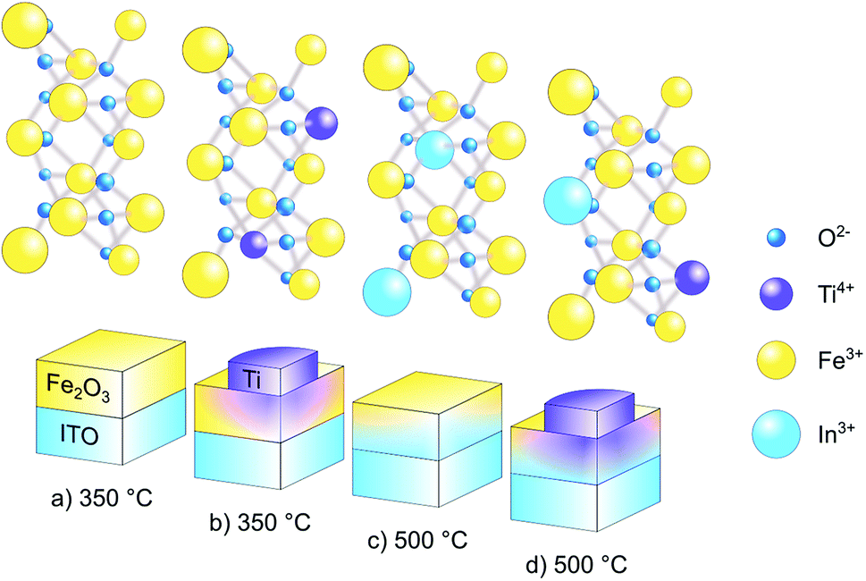 | ||
| Fig. 1 Schematic representation of (a) pure α-Fe2O3 layer, formed by annealing a 10 nm thick Fe layer on ITO at 350 °C (b) ex situ Ti4+ doping in pure α-Fe2O3 by the deposition of Ti nanodisks followed by annealing at 350 °C (c) in situ In3+ doping in α-Fe2O3 by diffusion of In from ITO to hematite at 500 °C annealing temperature and (d) ex situ Ti4+ doping in In3+ doped α-Fe2O3 by the deposition of Ti nanodisks followed by annealing at 350 °C. | ||
A 10 nm thick Fe layer, when annealed at 350 °C, transforms into a ∼25 nm thick layer of pure α-Fe2O3, as confirmed by micro-Raman spectroscopy. The annealing at 500 °C results in some chemical and morphological change, marked by a shift in the Raman peak, visible in Fig. 2a. The Raman spectra collected on both the samples (Fig. 2a) exhibit five out of seven spectral signatures for α-Fe2O3 (221 (A1g), 285 (Eg), 396 (Eg), 479 (A1g) and 597 (Eg)).53 The 249 (Eg) and 302 (Eg) spectral signatures are most probably overlapped with the other peaks in Raman spectra, while the peaks associated with either maghemite or magnetite are not observed.54,55 This indicates that both annealing temperatures, 350 and 500 °C for 8 h, are suitable for transforming the Fe films to α-Fe2O3. The inset of Fig. 2a presents the Eg peak at 285 cm−1, where the blue-shifting and FWHM-broadening in the sample annealed at 500 °C are clearly visible. This blue shift in frequency and a corresponding broadening in FWHM of the phonon peaks represents a decreasing crystallite size.55 Further, the intensity of the Raman scattering is higher in the sample annealed at higher temperature (i.e. 500 °C): this is intuitive, as Raman scattering intensity is proportional to the number density of the interacting media.56 Therefore, the increase in the signal intensity in 500 °C annealed sample, as shown in the in-set of Fig. 2a, is an indication of higher film thickness and crystallinity in comparison to the sample annealed at 350 °C.
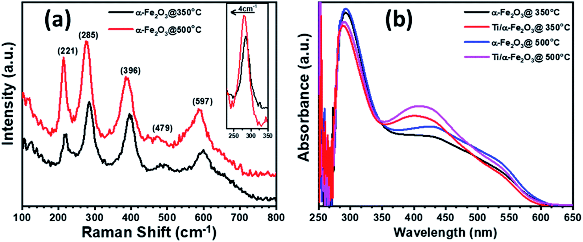 | ||
| Fig. 2 (a) Raman spectra for α-Fe2O3 thin films annealed at 350 °C and 500 °C-for 8 h, (b) UV-Vis absorption spectra for α-Fe2O3 thin films annealed at 350 °C and 500 °C and further modified by Ti nanodisks. | ||
The optical absorption behavior of hematite samples, as prepared and modified by Ti doping, were characterized by UV-vis absorption in the wavelength range 250–650 nm (Fig. 2b). The absorbance spectra in the samples, annealed at 350 and 500 °C, are similar to each other below 350 nm wavelength, except in the 350–600 nm as the samples annealed at 500 °C exhibit more absorption in this wavelength range. This increased absorption in the visible region is probably due to the slightly higher film thickness in samples annealed at 500 °C, and to the diffusion of substrate impurities (discussed in detail in XPS section);57 such increase is known to happen in In-doped hematite films.45 Further, doping with Ti4+ in both pristine and In-diffused α-Fe2O3 further increases the optical absorption in the wavelength range 350–485 nm, indicating stronger absorption,45,58 and showing an apparent blue-shift of the visible-light absorption peak. This enhancement could be attributed to the addition of the 5 nm thickness over the hematite surface for the incorporation of Ti4+ ions, which might increase the overall thickness of the hematite film after annealing at 350 °C.59 However, Ti doping and In/Ti co-doping in hematite show slightly weaker absorption at a lower wavelength, probably due to the oxidation of Ti to TiO2 which is a wide band gap material and able to absorb UV light. The absorption peak centered around 390–420 nm is assigned to a direct transition O−2(2p) → Fe3+(3d) in hematite, caused by holes generated at oxygen sites, while the broader peak between 500 and 600 nm is assigned to an indirect transition Fe3+(3d) → Fe3+(3d) (spin flip), caused by holes generated at iron sites.60,61 The apparent shift caused by the titanium doping can be justified by an efficiency increase of the first type of transition, while the second type maintains its initial absorption.62,63 All the samples exhibit a gradual decrease in absorbance until 610 nm, corresponding to a 2.02 eV bandgap, which is within the range usually reported for hematite (2.0–2.2 eV).
To analyze the structural and optical results we further characterize the hematite samples for surface morphology by FE-SEM and HR-TEM, and also performed EDX analysis in TEM to see any potential difference in the chemical composition with respect to the annealing temperature. Fig. 3a and b show the FE-SEM images for the samples prepared at 350 °C and 500 °C, respectively. The annealing temperature has a significant effect on surface morphology: the sample annealed at 350 °C shows a flat granular surface with nano-sized grains. In contrast, the sample annealed at 500 °C shows a flaky structure with high surface roughness, which might increase the effective electrode–electrolyte surface area and therefore enhance the total photocurrent density.39 Cross-section TEM micrographs show the formation of dense α-Fe2O3 films, with thicknesses of approximately 25 nm and 27 nm for the samples prepared at 350 and 500 °C, respectively. The samples annealed at 500 °C exhibit high crystallinity and slightly higher thickness (27 nm) as compared to samples annealed at 350 °C. These results support the blue shifting and increase in peak intensity in Raman spectra for the samples annealed at 500 °C. In order to verify the diffusion of substrate impurities into the hematite thin films, EDX analysis installed in TEM was carried out, as shown in ESI Fig. S1(1-c).†
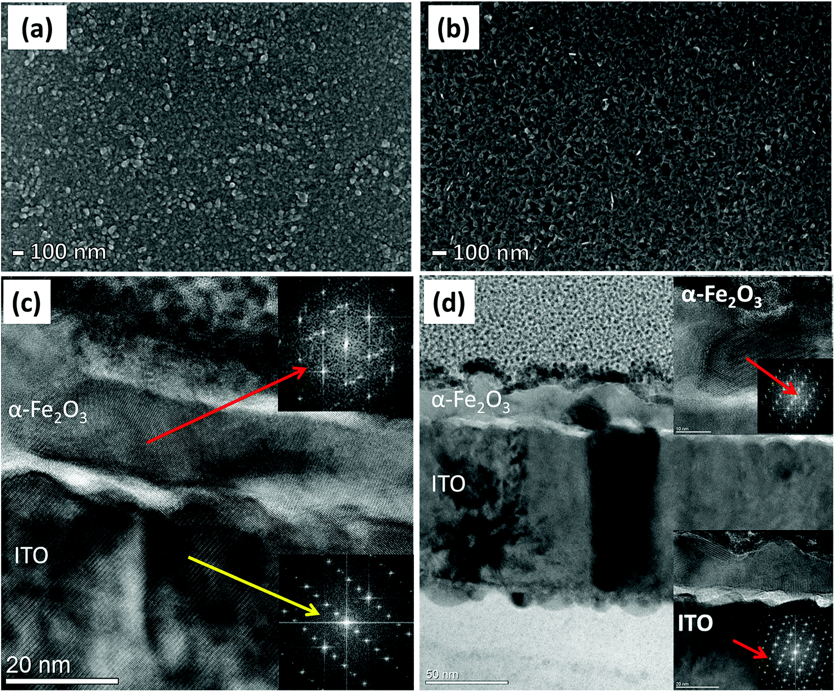 | ||
| Fig. 3 FE-SEM images of α-Fe2O3 thin films annealed at (a) 350 °C and (b) 500 °C. TEM and HR-TEM images of α-Fe2O3 thin films annealed at (c) 350 °C and (d) 500 °C. | ||
To further analyze the chemical composition, in relation to both annealing temperature and Ti doping, we characterized the samples by XPS. Fig. 4 shows the XPS plots collected on all four samples. Survey spectra (Fig. S2†) of α-Fe2O3 samples prepared at 350 and 500 °C mainly display the peaks corresponding to Fe, O and C.64 Surprisingly, a few additional peaks, at 444 and 45 eV, were detected, corresponding to In(3d) in the samples prepared at 500 °C, but not in the samples prepared at 350 °C.38,64 This strongly implies that In atoms are diffusing from the ITO substrate into the α-Fe2O3 layer at the higher sintering temperature, where they act as electron donating substitutional impurities. Fig. 4a shows the XPS spectra of the Fe(2p) core level, obtained from both α-Fe2O3 samples: it is evident the Fe(2p) orbital splitting due to spin orbit interaction, resulting in Fe(2p3/2) and Fe(2p1/2) states.65 The Fe(2p3/2) peak in both samples was obtained at a binding energy of ∼711.0 eV (Fig. 4a), consistently with the typical values observed for hematite.66 The energy separation between Fe(2p3/2) and Fe(2p1/2) (Δ = 13.5 eV) in both samples clearly supports the formation of pure Fe(III) oxide, as was already indicated by Raman spectroscopy.66 In the case of Ti doping, the absence of any additional satellite peaks related to Fe2+ at 730 or 715 eV indicates that Fe2+ does not exist at the surface on doped samples after Ti doping.58 The O 1s XPS spectrum (Fig. 4b) exhibits two peaks at around 529.3 and 531.6 eV in all samples: the first peak, can be attributed to Fe–O bonds (lattice O2−) in hematite, while the second peak is clearly variable with respect to the treatment of each sample. The peak can be assigned to O− (Vo), which is developed due to loss of oxygen, creation of oxygen vacancies or presence of absorbed OH− in the samples.58,67 The effect appears in the sample that undergoes only annealing at 500 °C; in the sample annealed at 350 °C and doped with Ti a further growth of the peak is visible, alongside a broadening around 553.5 eV, which is due to adsorbed water on the surface. Finally, the sample annealed at 500 °C and doped with Ti expands on both peaks, suggesting the creation of more oxygen vacancies and the adsorption of more water molecules.68,69 The indium core level XPS measurements are visible in Fig. 4c, showing that a significant amount of In was detected on the surface of hematite samples annealed at 500 °C. However, no signals of these substrate impurities were detected in the hematite samples annealed at 350 °C, which indicates that there was no diffusion of In atoms at the lower temperature. Fig. 4c displays the peaks at binding energies of 451.7 eV and 444.2 eV, which are assigned to In 3d3/2 and In 3d5/2.64 These peaks are especially relevant, because they confirm the existence of In on the surface of hematite, demonstrating that In3+ atoms, acting as a co-dopant, have diffused effectively into the sample, as a consequence of the high-temperature annealing. However, the Ti dopant is in a +4 state, as noted by the peaks at binding energies 463.7 and 458.2 eV (Fig. 4d), allocated respectively to Ti 2p1/2 and Ti 2p3/2,44,58 with no detectable difference between the Ti spectra after annealing at the two different temperatures.
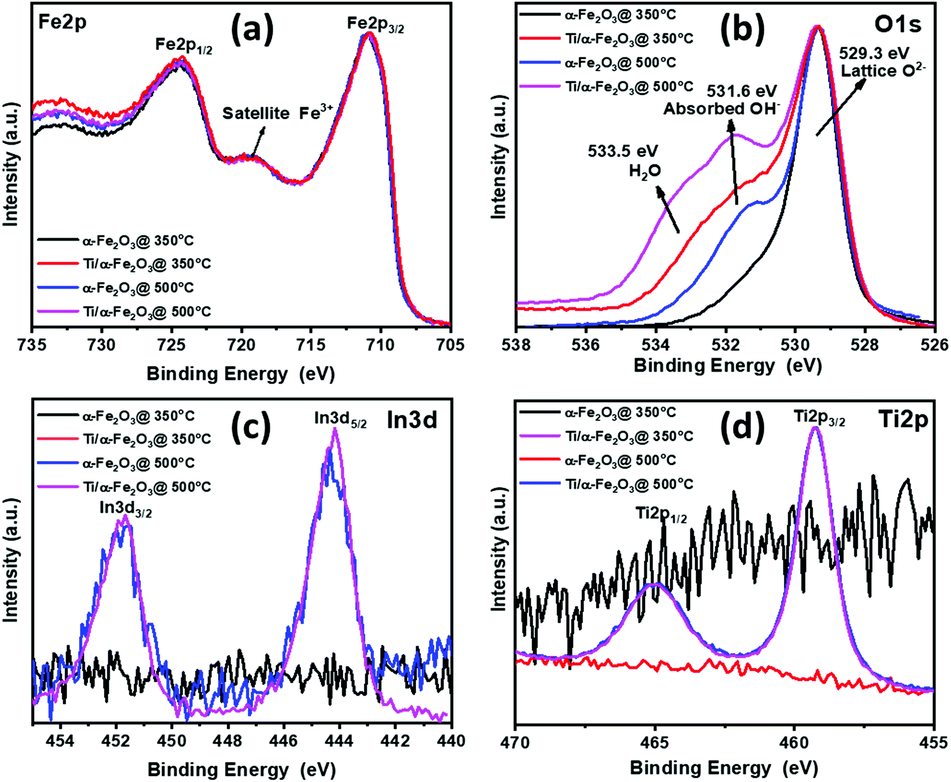 | ||
| Fig. 4 XPS core level spectra for (a) Fe 2p (b) O 1s (c) In 3d and (d) Ti 2p recorded on α-Fe2O3 annealed at 350 °C and 500 °C and further modified by Ti nanodisks. | ||
3.2 Photoelectrochemical behavior
The photoelectrochemical performance of the prepared photoanodes was investigated by photocurrent density–potential (Jph–VRHE) characteristics, with the current density–time (Jph–t) transient response testing, by the incident-photon-to-current (IPCE) conversion efficiency, and by Mott–Schottky and electrochemical impedance measurements. Fig. 5a shows the PEC performance in terms of Jph–VRHE characteristic curves measured in a 0.1 M NaOH electrolyte. The potential of the hematite photoanodes was swept at a scan rate of 10 mV s−1 from cathodic to anodic potentials, both under the dark and under 1 sun AM 1.5 G illumination. For the two hematite photoanodes produced after annealing Fe films at 350 and 500 °C, it is noticeable that under dark conditions (dashed lines), the water oxidation onset potential for both samples is almost the same, i.e. 1.70 VRHE (as calculated from the Butler plots shown in Fig. S3†); at higher potentials, a sharp increase in the dark current was observed in the samples prepared at 350 °C, whereas the high temperature annealing of Fe film for making α-Fe2O3 photoanode shows a poor water oxidation performance under dark condition. Under illumination, the α-Fe2O3 photoanode prepared at 350 °C exhibited a late Vonset of ca. 1.15 VRHE, with a poor photocurrent response of ca. 37 μA cm−2 at 1.23 VRHE. However, the photocurrent was observed to increase sharply to more than 315 μA cm−2 at an anodic potential of 1.5 VRHE. Diffusion of In from the ITO substrate to α-Fe2O3 layer at 500 °C improved the PEC performance of the ultrathin α-Fe2O3 photoanode by exhibiting a slightly lower cathodic Vonset of ca. 1.12 VRHE, but with a much higher photocurrent response of ca. 145 μA cm−2 at 1.23 VRHE. Also, the photocurrent plateau is reached at 1.50 VRHE with a photocurrent of ca. 398 μA cm−2, which is significantly higher than that of the pristine α-Fe2O3 photoanode prepared at the annealing temperature of 350 °C (<315 μA cm−2). This demonstrates that the PEC performance of the hematite photoanode is significantly improved when In is diffused to α-Fe2O3 films from under ITO substrate. In addition, the two samples produced with the addition of Ti nanodisks show that doping the α-Fe2O3 with Ti leads to a notable increase in photocurrent density: at 1.23 VRHE, the photocurrent density of the α-Fe2O3 sample doped with Ti (by annealing at 350 °C) reaches 70 μA cm−2 at 1.23 VRHE and 550 μA cm−2 at 1.50 VRHE, which is a 2 times higher value than that for the pure α-Fe2O3. The larger photocurrent can be attributed to the improvement of light harvesting and the enhancement of electrical conductivity derived from the incorporation of Ti-dopants into hematite nanostructure.24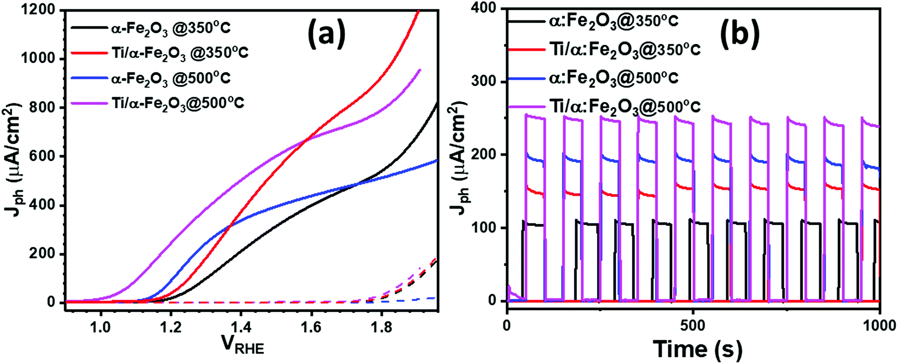 | ||
| Fig. 5 (a) Photocurrent density–potential curves (b) transient photocurrent measurement for the water oxidation reaction for α-Fe2O3 thin films annealed at 350 °C and 500 °C and Ti doped α-Fe2O3 annealed at 350 °C and 500 °C under 1 sun illumination at 1.23 V vs. VRHE. | ||
Finally, In/Ti co-doped α-Fe2O3 (annealed at 500 °C) shows the maximum photocurrent density, giving a value of 290 μA cm−2 at 1.23 VRHE and 602 μA cm−2 at 1.50 VRHE, which is around 9-fold increase to that of pure α-Fe2O3 film at 1.23 VRHE and about 2- and 5-fold increase to that of In-doped and Ti-doped α-Fe2O3 photoanode, respectively. It is noteworthy that the onset potential of the photocurrent for In/Ti co-doped α-Fe2O3 also shifted cathodically, which would benefit the PEC water splitting at lower voltage. The negative shift of the onset potentials demonstrates a more efficient interfacial charge transfer that prevents the hole accumulation at the electrode surface and thus decreases surface charge recombination. We also performed the IPCE measurement on pristine and In-doped α-Fe2O3 photoanodes at various wavelengths, as shown in ESI Fig. S4.† Pristine α-Fe2O3 photoanodes exhibit an IPCE value of 8% at 375 nm; however, In3+ doped α-Fe2O3 photoanodes exhibit a higher IPCE, of around 12% at the same wavelength. These IPCE results are consistent with the difference in photocurrent densities as observed in pristine and In-doped α-Fe2O3 photoanodes. From the transient photocurrents measurements at a constant potential (1.23 VRHE) in Fig. 5b, it appears that the current decay (Id) (the difference between initial current (Ii) and final current (If); Id = Ii − If) increased from 5 μA cm−2 pure α-Fe2O3 photoanode to 12 μA cm−2 for Ti/In co-doped photoanode. Beyond that, all samples are prompt in generating a reproducible response to light on–off cycles, indicating that a quick charge transport process can be achieved. When exposing to 1000 s illumination, the In/Ti-co-doped α-Fe2O3 photoanode shows excellent stability with up to 98% retention of its initial photocurrent density. Additionally, in comparison to single element doped α-Fe2O3 photoanodes, the co-doped α-Fe2O3 photoanodes exhibited excellent photochemical stability and photochemical response (Fig. 6b).
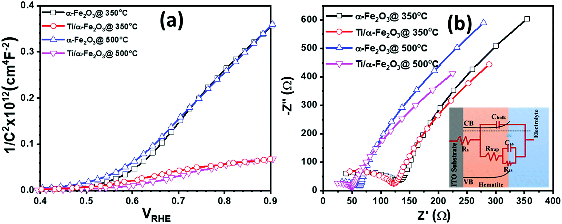 | ||
| Fig. 6 (a) Mott–Schottky plots, (b) electrochemical impedance spectra for pristine (black, square markers), Ti doped (red, round markers), In doped (blue, upward triangle markers) and In/Ti co-doped (magenta, downward triangle markers) α-Fe2O3 thin films. | ||
Further, we performed Mott–Schottky measurement on all the samples under dark condition and measured the capacitance at the photoanode-electrolyte surface, in order to drive the Mott–Schottky curves to obtain the interface properties between the active material and electrolyte. The obtained Mott–Schottky curves (1/C2 versus VRHE) were used to determine the donor density (Nd) and flat-band potential (Vfb) by using the Mott–Schottky equation: C−2 = (2/qεoεsNd)[V − Vfb − kT/q], where εo is the permittivity of the vacuum, εs is the dielectric constant of the hematite (in case of α-Fe2O3, εs is 80), q is the electronic charge and kT/q is the thermal voltage (26 meV at room temperature).70 The value of Vfb was calculated from the intercept of the straight line to the x-axis in the linear region of the Mott–Schottky plots. The values of Nd were calculated by taking a linear region of the slope between 0.60 and 1.00 VRHE and by considering the geometrical electrode area only by using the equation, Nd = 2/(εoεsq)[d(1/C2)/dV]−1. Fig. 6a shows the Mott–Schottky plots for all the samples; the values of flat-band potential (Vfb) and donor density (Nd) derived from these plots are summarized in Table S1.† From the slope of the Mott–Schottky plots it can be seen that the α-Fe2O3 sample prepared at two different annealing temperature of 350 °C (pristine α-Fe2O3) and 500 °C (In doped α-Fe2O3) have a very similar slope, indicating that Vfb and Nd in both samples correspond to similar values. The pristine hematite sample exhibits a Vfb value of 0.55 VRHE and Nd of 8.78 × 1018 cm−3. However, a shift in Vfb to 0.51 VRHE and a minor increase in Nd up to 9.90 × 1018 cm−3 was calculated for the In doped α-Fe2O3 sample prepared at 500 °C annealing temperature. A slight increase in Nd and change in Vfb in In doped α-Fe2O3 photoanode is probably due to the change in surface morphology and relatively higher thickness of α-Fe2O3 layer annealed at 500 °C. However, unlike the sample annealed at 350 °C, the sample annealed at 500 °C shows a noticeable curvature above the flat-band potential (Fig. 6a). This curvature might originate from the nanostructured morphology caused by the higher annealing temperature, leading to a higher true electrode–electrolyte contact area.60 In general, the Mott–Schottky equation is derived by assuming a perfectly flat electrode surface.60 From the SEM images, we can see the changes in the surface morphology (Fig. 3a and b), where the sample annealed at 500 °C shows the formation of nanostructures on the surface. In the case of Ti4+ doping through making the disks with 40 nm in diameter and 5 nm in thickness following by air annealing at 350 °C, the slope and curvature of the Mott–Schottky plots increases significantly. The increases of slope and curvature in Mott–Schottky plots with Ti4+ doping suggests that both the carrier concentration and surface roughness is increasing. The Ti doping in pristine hematite sample exhibits a Vfb value of 0.52 VRHE and Nd of 9.46 × 1018 cm−3. However, a further shift in Vfb to 0.49 VRHE and increase in Nd up to 9.97 × 1018 cm−3 was calculated for the In/Ti4+ co-doped α-Fe2O3 sample.
To further understand the role of dopant, electrochemical impedance spectroscopy (EIS) analysis was adopted, as shown in Fig. 6b. The equivalent circuit adopted to fit EIS data is given in the inset of Fig. 6b. Rtrap represents the resistance for surface-state trapping of holes and electrons, and Rss describes the surface-state resistance of the charge transfer of holes to reducers in solution. The capacitance of the space charge, as well as a connection of Helmholtz capacitance, are integrated into Cbulk. Besides, Css denotes the surface-state capacitance, and Rs is the series resistance of the electrode–electrolyte setup.71 Although no significant differences could be observed of Rs, Cbulk, and Css, the reduction of Rtrap and Rss is clearly seen upon incorporating the In-dopant into the pristine hematite. This indicates that the surface recombination of holes and electrons is reduced by In-dopant, further by Ti-dopant, and the charge transfer of holes to reducers in solution is fostered. The ameliorated surface reaction may explain the improved PEC performance of Ti doped hematite, and In/Ti co-doped hematite.72,73
4. Conclusions
To summarize, co-doping of indium and titanium in ultra-thin hematite films display an overall improvement of all the parameters that characterize water splitting efficacy. These results, paired with the chemical and physical characterization, indicate that this type of co-doping treatment transforms the film by affecting both the carrier density and the surface topology. Further, this study presents a straightforward method for doping and/or co-doping in hematite thin films, effectively improving the photoelectrochemical performance in terms of both photocurrent density, onset voltage and IPCE, and it provides insight on the structural and chemical changes brought by the dopant. In particular, the latter (chemical changes) provide the scientific community with new information for further improving the performance of solar water splitting devices without increasing their cost or the carbon footprint of their fabrication.Conflicts of interest
The authors declare no conflict of interest.Acknowledgements
We gratefully acknowledge the financial support provided by the Swedish Research Council Formas and the Academy of Finland, project numbers 287011, 319018. C. T. acknowledges the financial support of the Yrjö, Vilho ja Kalle Väisälä Foundation grant issued by the Finnish Academy of Sciences and Letters. We also acknowledge the provision of facilities and technical support from Micronova Nanofabrication Centre at Aalto University and Myfab Chalmers.References
- S. Chu, W. Li, Y. Yan, T. Hamann, I. Shih, D. Wang and Z. Mi, Nano Futures, 2017, 1, 022001 CrossRef.
- B. A. Pinaud, J. D. Benck, L. C. Seitz, A. J. Forman, Z. Chen, T. G. Deutsch, B. D. James, K. N. Baum, G. N. Baum, S. Ardo, H. Wang, E. Miller and T. F. Jaramillo, Energy Environ. Sci., 2013, 6, 1983–2002 RSC.
- K. T. Fountaine, H. J. Lewerenz and H. A. Atwater, Nat. Commun., 2016, 7, 1–9 Search PubMed.
- K. Sivula, F. Le Formal and M. Grätzel, ChemSusChem, 2011, 4, 432–449 CrossRef CAS.
- S. Keene, R. B. Chandran and S. Ardo, Energy Environ. Sci., 2019, 12, 261–272 RSC.
- Y. Chen, X. Feng, Y. Liu, X. Guan, C. Burda and L. Guo, ACS Energy Lett., 2020, 5, 844–866 CrossRef CAS.
- Y. Yang, S. Niu, D. Han, T. Liu, G. Wang and Y. Li, Adv. Energy Mater., 2017, 7, 1700555 CrossRef.
- Y. He, T. Hamann and D. Wang, Chem. Soc. Rev., 2019, 48, 2182–2215 RSC.
- C. Tossi, L. Hällström, J. Selin, M. Vaelma, E. See, J. Lahtinen and I. Tittonen, J. Mater. Chem. A, 2019, 7, 14519–14525 RSC.
- K. M. H. Young, B. M. Klahr, O. Zandi and T. W. Hamann, Catal. Sci. Technol., 2013, 3, 1660–1671 RSC.
- A. G. Tamirat, J. Rick, A. A. Dubale, W.-N. Su and B.-J. Hwang, Nanoscale Horiz., 2016, 1, 243–267 RSC.
- M. Ashraf, I. Khan, M. Usman, A. Khan, S. S. Shah, A. Z. Khan, K. Saeed, M. Yaseen, M. F. Ehsan, M. N. Tahir and N. Ullah, Chem. Res. Toxicol., 2020, 33, 1292–1311 Search PubMed.
- R. van de Krol, Y. Liang and J. Schoonman, J. Mater. Chem., 2008, 18, 2311–2320 RSC.
- B. Iandolo, B. Wickman, I. Zorić and A. Hellman, J. Mater. Chem. A, 2015, 3, 16896–16912 RSC.
- A. Kay, I. Cesar and M. Grätzel, J. Am. Chem. Soc., 2006, 128, 15714–15721 CrossRef CAS.
- X. Yang, R. Liu, C. Du, P. Dai, Z. Zheng and D. Wang, ACS Appl. Mater. Interfaces, 2014, 6, 12005–12011 CrossRef CAS.
- A. P. Singh, N. Saini and B. R. Mehta, ChemistrySelect, 2017, 2, 1413–1420 CrossRef CAS.
- P. Tang and J. Arbiol, Nanoscale Horiz., 2019, 4, 1256–1276 RSC.
- A. Azad and S.-J. Kim, Glass Phys. Chem., 2016, 42, 458–472 CrossRef CAS.
- K. D. Malviya, H. Dotan, D. Shlenkevich, A. Tsyganok, H. Mor and A. Rothschild, J. Mater. Chem. A, 2016, 4, 3091–3099 RSC.
- M. Li, J. Deng, A. Pu, P. Zhang, H. Zhang, J. Gao, Y. Hao, J. Zhong and X. Sun, J. Mater. Chem. A, 2014, 2, 6727–6733 RSC.
- N. Li, S. Jayaraman, S. Y. Tee, P. S. Kumar, C. J. J. Lee, S. L. Liew, D. Chi, T. S. A. Hor, S. Ramakrishna and H.-K. Luo, J. Mater. Chem. A, 2014, 2, 19290–19297 RSC.
- K. Sivula, R. Zboril, F. Le Formal, R. Robert, A. Weidenkaff, J. Tucek, J. Frydrych and M. Grätzel, J. Am. Chem. Soc., 2010, 132, 7436–7444 CrossRef CAS.
- R. Franking, L. Li, M. A. Lukowski, F. Meng, Y. Tan, R. J. Hamers and S. Jin, Energy Environ. Sci., 2013, 6, 500–512 RSC.
- J.-W. Jang, C. Du, Y. Ye, Y. Lin, X. Yao, J. Thorne, E. Liu, G. McMahon, J. Zhu, A. Javey, J. Guo and D. Wang, Nat. Commun., 2015, 6, 1–5 Search PubMed.
- N. J. Cherepy, D. B. Liston, J. A. Lovejoy, H. Deng and J. Z. Zhang, J. Phys. Chem. B, 1998, 102, 770–776 CrossRef CAS.
- H. Pan, X. Meng and G. Qin, Phys. Chem. Chem. Phys., 2014, 16, 25442–25448 RSC.
- J. Y. Kim, G. Magesh, D. H. Youn, J.-W. Jang, J. Kubota, K. Domen and J. S. Lee, Sci. Rep., 2013, 3, 1–8 Search PubMed.
- S. Ho-Kimura, B. A. D. Williamson, S. Sathasivam, S. J. A. Moniz, G. He, W. Luo, D. O. Scanlon, J. Tang and I. P. Parkin, ACS Omega, 2019, 4, 1449–1459 CrossRef CAS.
- Y. Ling, G. Wang, D. A. Wheeler, J. Z. Zhang and Y. Li, Nano Lett., 2011, 11, 2119–2125 CrossRef CAS.
- H. C. Nguyën, F. A. Garcés-Pineda, M. de Fez-Febré, J. R. Galán-Mascarós and N. López, Chem. Sci., 2020, 11, 2464–2471 RSC.
- M. J. Kang and Y. S. Kang, J. Mater. Chem. A, 2015, 3, 15723–15728 RSC.
- F. L. Formal, N. Tétreault, M. Cornuz, T. Moehl, M. Grätzel and K. Sivula, Chem. Sci., 2011, 2, 737–743 RSC.
- N. Bhandary, A. P. Singh, P. P. Ingole and S. Basu, RSC Adv., 2016, 6, 35239–35247 RSC.
- X. Zhao, J. Feng, N. Wang, X. Yao, W. Chen, S. Chen, Z. Huang and Z. Chen, Energy Technol., 2018, 6, 2188–2199 CrossRef CAS.
- S. D. Tilley, M. Cornuz, K. Sivula and M. Grätzel, Angew. Chem., 2010, 122, 6549–6552 CrossRef.
- T.-Y. Yang, H.-Y. Kang, K. Jin, S. Park, J.-H. Lee, U. Sim, H.-Y. Jeong, Y.-C. Joo and K. T. Nam, J. Mater. Chem. A, 2014, 2, 2297–2305 RSC.
- W. R. W. Ahmad, M. H. Mamat, A. S. Zoolfakar, Z. Khusaimi and M. Rusop, in 2016 IEEE Student Conference on Research and Development (SCOReD), 2016, pp. 1–6 Search PubMed.
- M. Marelli, A. Naldoni, A. Minguzzi, M. Allieta, T. Virgili, G. Scavia, S. Recchia, R. Psaro and V. Dal Santo, ACS Appl. Mater. Interfaces, 2014, 6, 11997–12004 CrossRef CAS.
- N. Bhandary, A. P. Singh, P. P. Ingole and S. Basu, ChemPhotoChem, 2017, 1, 70–75 CrossRef CAS.
- P. Qiu, H. Yang, L. Yang, Q. Wang and L. Ge, Electrochim. Acta, 2018, 266, 431–440 CrossRef CAS.
- Origin of High-Efficiency Photoelectrochemical Water Splitting on Hematite/Functional Nanohybrid Metal Oxide Overlayer Photoanode after a Low Temperature Inert Gas Annealing Treatment, ACS Omega, 2020, DOI:10.1021/acsomega.8b02444.
- X. Yang, R. Liu, Y. Lei, P. Li, K. Wang, Z. Zheng and D. Wang, ACS Appl. Mater. Interfaces, 2016, 8, 16476–16485 CrossRef CAS.
- A. Srivastav, A. Verma, A. Banerjee, S. A. Khan, M. Gupta, V. R. Satsangi, R. Shrivastav and S. Dass, Phys. Chem. Chem. Phys., 2016, 18, 32735–32743 RSC.
- S. Krehula, M. Ristić, M. Reissner, S. Kubuki and S. Musić, J. Alloys Compd., 2017, 695, 1900–1907 CrossRef CAS.
- F. F. Abdi, L. Han, A. H. M. Smets, M. Zeman, B. Dam and R. van de Krol, Nat. Commun., 2013, 4, 1–7 Search PubMed.
- Z. Luo, C. Li, S. Liu, T. Wang and J. Gong, Chem. Sci., 2016, 8, 91–100 RSC.
- D. Chen and Z. Liu, ChemSusChem, 2018, 11, 3438–3448 CrossRef CAS.
- A. Annamalai, H. H. Lee, S. H. Choi, S. Y. Lee, E. Gracia-Espino, A. Subramanian, J. Park, K. Kong and J. S. Jang, Sci. Rep., 2016, 6, 1–11 CrossRef.
- Y. Makimizu, J. Yoo, M. Poornajar, N. T. Nguyen, H.-J. Ahn, I. Hwang, S. Kment and P. Schmuki, J. Mater. Chem. A, 2020, 8, 1315–1325 RSC.
- B. Iandolo, B. Wickman, B. Seger, I. Chorkendorff, I. Zorić and A. Hellman, Phys. Chem. Chem. Phys., 2014, 16, 1271–1275 RSC.
- M. R. Shaner, K. T. Fountaine and H.-J. Lewerenz, Appl. Phys. Lett., 2013, 103, 143905 CrossRef.
- K. Sekizawa, K. Oh-ishi, K. Kataoka, T. Arai, T. M. Suzuki and T. Morikawa, J. Mater. Chem. A, 2017, 5, 6483–6493 RSC.
- M. Hanesch, Geophys. J. Int., 2009, 177, 941–948 CrossRef CAS.
- A. M. Jubb and H. C. Allen, ACS Appl. Mater. Interfaces, 2010, 2, 2804–2812 CrossRef CAS.
- R. R. Jones, D. C. Hooper, L. Zhang, D. Wolverson and V. K. Valev, Nanoscale Res. Lett., 2019, 14, 231 CrossRef.
- W. J. Shin, A. H. Granados, W.-H. Huang, H. Hu and M. Tao, Mater. Chem. Phys., 2019, 222, 152–158 CrossRef CAS.
- Q. Wu, D. Meng, Y. Zhang, Q. Zhao, Q. Bu, D. Wang, X. Zou, Y. Lin, S. Li and T. Xie, J. Alloys Compd., 2019, 782, 943–951 CrossRef CAS.
- D. Cao, W. Luo, M. Li, J. Feng, Z. Li and Z. Zou, CrystEngComm, 2013, 15, 2386–2391 RSC.
- I. Cesar, K. Sivula, A. Kay, R. Zboril and M. Grätzel, J. Phys. Chem. C, 2009, 113, 772–782 CrossRef CAS.
- L. A. Marusak, R. Messier and W. B. White, J. Phys. Chem. Solids, 1980, 41, 981–984 CrossRef CAS.
- N. Uekawa, M. Watanabe, K. Kaneko and F. Mizukami, J. Chem. Soc., Faraday Trans., 1995, 91, 2161–2166 RSC.
- S. Kumari, A. P. Singh, Sonal, D. Deva, R. Shrivastav, S. Dass and V. R. Satsangi, Int. J. Hydrogen Energy, 2010, 35, 3985–3990 CrossRef CAS.
- C. D. Wagner, W. M. Riggs, L. E. Davis and J. F. Moulder, Handbook of X-ray photoelectron spectroscopy, PerkinElmer Corporation, Physical Electronics Division, Eden Prairie, Minnesota, USA, 1979 Search PubMed.
- A. P. Grosvenor, B. A. Kobe, M. C. Biesinger and N. S. McIntyre, Surf. Interface Anal., 2004, 36, 1564–1574 CrossRef CAS.
- E. Soo Cho, M. Jong Kang and Y. Soo Kang, Phys. Chem. Chem. Phys., 2015, 17, 16145–16150 RSC.
- X. Zhang, X. Wang, X. Yi, J. Ye and D. Wang, Alkali, ACS Sustainable Chem. Eng., 2019, 7, 5420–5429 CrossRef CAS.
- S. W. Knipe, J. R. Mycroft, A. R. Pratt, H. W. Nesbitt and G. M. Bancroff, Geochim. Cosmochim. Acta, 1995, 59, 1079–1090 CrossRef CAS.
- Z. Jakub, F. Kraushofer, M. Bichler, J. Balajka, J. Hulva, J. Pavelec, I. Sokolović, M. Müllner, M. Setvin, M. Schmid, U. Diebold, P. Blaha and G. S. Parkinson, ACS Energy Lett., 2019, 4, 390–396 CrossRef CAS.
- B. Klahr, S. Gimenez, F. Fabregat-Santiago, T. Hamann and J. Bisquert, J. Am. Chem. Soc., 2012, 134, 4294–4302 CrossRef CAS.
- B. Iandolo, H. Zhang, B. Wickman, I. Zorić, G. Conibeer and A. Hellman, RSC Adv., 2015, 5, 61021–61030 RSC.
- B. Iandolo and A. Hellman, Angew. Chem., Int. Ed., 2014, 53, 13404–13408 CrossRef CAS.
- A. Hellman, B. Iandolo, B. Wickman, H. Grönbeck and J. Baltrusaitis, Surf. Sci., 2015, 640, 45–49 CrossRef CAS.
Footnote |
| † Electronic supplementary information (ESI) available. See DOI: 10.1039/d0ra04576d |
| This journal is © The Royal Society of Chemistry 2020 |