
 Open Access Article
 This Open Access Article is licensed under a Creative Commons Attribution-Non Commercial 3.0 Unported Licence
ZnO thin film-nanowire array homo-structures with tunable photoluminescence and optical band gap†
Yalambaku Rajesha,
Santanu Kumar Padhi b and
M. Ghanashyam Krishna*ac
b and
M. Ghanashyam Krishna*ac
aSchool of Physics, University of Hyderabad, Hyderabad-500046, Telangana, India. E-mail: mgksp@uohyd.ernet.in
bACRHEM, School of Physics, University of Hyderabad, Hyderabad-500046, Telangana, India
cCentre for Advanced Studies in Electronics Science and Technology, School of Physics, University of Hyderabad, Hyderabad-500046, Telangana, India
First published on 7th July 2020
Abstract
The growth and optical behavior of ZnO thin film-nanowire array homo-structures is reported. The ZnO films are deposited on glass substrates by thermal evaporation and subjected to heat treatment at 400 °C for 2 h to achieve crystallinity and stoichiometry. The surface comprises spherical grains or elongated flakes depending on thickness of films. These films are introduced in to a hydrothermal reactor in a medium of zinc acetate and HMTA to realize the nanostructures. The process results in the formation of ZnO nanowires with dimensions that are strongly dependent on the surface microstructure of the ZnO films. The role of temperature (90–180 °C) and duration (10 min to 10 h) of hydrothermal processing is investigated in detail. It is demonstrated that low temperature and short duration are ideal for producing nanowires with diameter < 100 nm, while longer durations and higher temperatures lead to large diameter and long length nanowires. Interestingly, all wires converge to a hexagonal shape with increase in duration or temperature. The lowest diameter of the vertically aligned nanowires is 50 nm and length upto 10 μm is achieved. Optical band gap of the homo-structures is of the order of 3.4–3.5 eV. Raman and photoluminescence spectra indicate the presence of defects in the films. The thin films exhibit a strong defect related photoluminescence peak centred around 550 nm. The nanowires grown on the films display both the UV-near band edge peak as well as the defect related peak. However, the intensity of the defect peak decreases with increase in length of the nanowires indicating that the photoluminescence of the homo-structures can be tuned by changing the surface microstructure of the films and also the aspect ratio of the nanowires.
1. Introduction
Zinc oxide (ZnO) is a wide band-gap (3.37 eV) II–VI semiconductor that has attracted interest as an electronic material for numerous applications such as solar cells, piezoelectric devices, transparent conducting electrodes, chemical sensors, catalysis, light emitting diodes, actuation and optoelectronic devices. In recent years, many methods have been used to synthesize ZnO material as one-dimensional (1D) nanostructures with different morphologies including nanowires, nanorods, nanoneedles, nanorings, quantum dots and other superstructures.1–9There has been interest in the fabrication of ZnO based homo-junctions for photoluminescence and light emitting diode applications.10–16 Sun et al.10 reported good light emission properties in a homo-structure comprising p-ZnO film/n-ZnO nanowire with turn-on voltage around 8 V. In this case the ZnO film was grown by spray pyrolysis while the nanowires were hydrothermally processed. Su et al.11 demonstrated that homo-junctions of Sb doped ZnO nanowires grown by CVD technique on single crystal Ga doped ZnO substrates have a low turn on voltage and sharp near band edge emission. Kampylafka et al.12 demonstrated fabrication of p and n-type ZnO thin film based homo-junctions with turn-on voltage of the order of 1.5 V and transmittance of 75–85%. The ZnO thin films are prepared by RF sputter deposition. Baek et al.13 demonstrated Sb doped ZnO nanorod array-based homo-junctions for LED applications with a turn on voltage of 3.7 V and near band edge emission accompanied by a peak centred around 730 nm. In this work, the ZnO nanorods are grown by hydrothermal synthesis while the thin films are deposited by RF sputtering. Geng et al. have grown ZnO nanowires by hydrothermal synthesis on e-beam evaporated Ag and ZnO films and demonstrated tunability of photoluminescence.14 These few examples indicate that such structures possess several advantages over more conventional heterostructures due to the ease of fabrication, fewer number of steps and control over growth patterns. As a consequence, they continue to generate interest for applications. The use of vacuum thermal evaporation, which is more cost effective and simpler than other physical vapour deposition processes, as a technique to prepare the ZnO films supporting the nanowire arrays has not been investigated. Another aspect that requires investigation is the effect of varying thickness and, hence, the surface of the ZnO thin films supporting the nanowire arrays on the properties of the homo-structures.
The objective of the present work is, therefore, the development of ZnO thin film-nanowire homo-junctions wherein the thin films (of thickness 100–400 nm) are deposited by thermal evaporation at room temperature (RT) followed by heat-treatment at 400 °C. The ZnO nanowire arrays are grown on these films by hydrothermal processing. Hydrothermal method has several advantages such as low process temperature, use of simple instrumentation, catalyst-free growth, low-cost, ease of large-scale production, eco-friendly and less hazardous.17–19 Therefore, the effect of thickness of films, temperature (90–180 °C) and duration of hydrothermal synthesis (processing) (10 min to 10 h) on the structure, microstructural evolution and optical behaviour is investigated. The novelty of the current approach lies in exploiting the advantage of such structures, by manipulating the dimensions of the nanowires as well as the microstructure of the thin films on which they are synthesized, to control photoluminescence emission wavelengths and intensities as well as the optical band gap.
2. Experimental
ZnO thin films of thickness 100–400 nm are deposited by thermal evaporation on glass substrates from a ZnO source. The substrates are first ultrasonically cleaned sequentially in solvents like acetone (99.8%), isopropanol (99.8%), and deionized water baths for about 10 min. Then, the substrates are dried with nitrogen gas after being kept at 100 °C for 5 min before the thin film deposition. A custom-built vacuum chamber equipped with diffusion and rotary pump are employed for the thermal evaporation. The base pressure is of the order of 10−6 mbar during evaporation, while the source to substrate separation and duration of ZnO evaporation are varied and four different thickness ZnO films are achieved. All the films are deposited at RT and subjected to post-deposition heat-treatment in air at 400 °C for 2 h.These ZnO thin film deposited substrates are then introduced into a hydrothermal reactor for growing different ZnO nanostructures. In a typical process run, these films are placed in a 100 mL teflon-liner stainless steel autoclave containing aqueous solution of 25 mM each of zinc acetate dehydrate [Zn(O2CCH3)2(H2O)2, 99.0% ZnAcD] and 25 mM hexamethylenetetramine (HMTA) [(CH2)6N4, 99.0%]. Experiments are also carried out at 15 mM (ZnAcD, precursor deficient) and 35 mM (ZnAcD, precursor rich) concentrations, maintaining the HMTA concentration at 25 mM. All chemicals are purchased from Sigma-Aldrich (Steinheim, Germany) and used without further purification. The duration of hydrothermal processing of ZnO(HP) is varied between 10 min to 10 h and temperatures are varied from 90 to 180 °C.
The thin film thickness is measured using a surface profilometer (model XP-1 Ambios Tech., USA). The surface microstructure investigation is carried out in a field emission scanning electron microscope (FE-SEM, Model Ultra55 of Carl Zeiss). The ZnO phase formation is confirmed by X-ray diffraction (XRD) patterns recorded in a powder X-ray diffractometer (Discover D8 diffractometer of Bruker, Germany) with Cu-Kα radiation (wavelength = 0.15408 nm). The Raman spectra are recorded in air using an Nd-YAG 532 nm laser in the back-scattering geometry in a CRM spectrometer equipped with a confocal microscope and 100× objective (model alpha 300 of WiTec Germany). The phase content within the samples are investigated in a spectral region of 200–1500 cm−1. Optical transmission spectra in the wavelength range of 200–2400 nm are measured by means of a dual-beam spectrophotometer (UV-vis-NIR, model, Jasco V-670) having a resolution limit of ±0.2 nm and a sampling interval of 2 nm. Fluorescence emission spectra are recorded on a Horiba Jobin Yvon model FL3-22 Fluorolog spectrofluorimeter.
3. Results and discussion
3.1 Microstructure and structure investigation of ZnO thin films
The surface microstructure of ZnO thin films of approximate thickness 100 nm, 150 nm, 200 nm and 400 nm is displayed in Fig. 1(a–d). The microstructure of the 100 nm thickness (Fig. 1(a)) ZnO film consists of densely packed spherical particles of diameter 30–50 nm. | ||
| Fig. 1 Scanning electron microscope images of ZnO thin films of (a) 100 nm, (b) 150 nm, (c) 200, and (d) 400 nm thickness respectively. | ||
The edges of the spherical particles are sharpened to give various non-spherical shapes, when thickness is increased to 150 nm (Fig. 1(b)). Few of the particles are elongated in one direction giving rectangular shapes. The elongation of these particles extended out of surface of the plane resulting in three dimensional (3D) microstructures. Due to this 3D arrangement, micron sized voids are developed at the interfaces. These particles transform into large spherical particles of 200 nm size, with increase in thickness of the films to 200 nm (Fig. 1(c)). This is accompanied by decrease in packing density of the particles as evidenced by the voids between them. The 400 nm thickness film has a completely different microstructure. The surface comprises of twisted flakes of length 30–50 nm and width of 400–500 nm that are vertically oriented. Thus, the ZnO film thickness increase has brought a profound change on the surface microstructural development and also the packing density of the evolved microstructures. The contribution of surface roughness to the evolution of the nanowires cannot be neglected.14 It would thus appear that variation in thickness causes changes in surface microstructure and roughness of the ZnO films. Apart from this, smaller grain size may lead to nanowires with smaller dimensions.14,20
The phase formation and crystallographic information of the thin films investigated using XRD are presented in Fig. 2(a–d). All diffraction peaks are indexed to ZnO with a hexagonal wurtzite crystal structure using JCPDS file no: 80-0074. This observation suggests that the changes in the thickness of ZnO thin films has modified the microstructure, but remain structurally phase pure. No un-reacted metallic Zn is observed. The prominent diffraction peaks at 2θ = 31.64, 34.12, 36.2 and 56.6° are indexed to (100), (002), (101) and (110) planes of hexagonal wurtzite phase of ZnO respectively.
 | ||
| Fig. 2 X-ray diffraction patterns of ZnO thin films of (a) 100 nm, (b) 150 nm, (c) 200 and (d) 400 nm thickness respectively. | ||
The very diffuse nature of peaks for the 100 nm samples can be attributed to the nanocrystalline nature of the films. There is a slight decrease in the relative intensities of the different ZnO peaks indicating change in the preferred orientation of the ZnO film. In the case of the 200 nm film, there is a relative drop in the intensity of (101) peak while, for the 400 nm film, there is increase in the peak intensity of (110) plane. It is significant that there are no peaks related to metallic Zn indicating that the films are stoichiometric ZnO (within the detection limits of XRD). It is known that crystallization of ZnO thin films prepared by thermal evaporation either from a Zn or ZnO source requires post-deposition heat treatment.21 The films in the present case are also nanocrystalline with crystallite size of 20–25 nm as estimated from Scherrer's formula. In addition, there is a shift in the peak positions to higher 2θ values with increase in thickness indicating a change in the residual stresses within the ZnO films at different thickness. These residual stresses are likely to originate from a mismatch in the thermal expansion coefficient of ZnO and glass substrate. Liu et al.22 attributed this deviation to surface effects which cause lattice deformations and reduction in the lattice parameter. This could also be the reason for the observed variations in microstructures as a function of thickness.
It is evident that the 100 nm ZnO film, thus, has comparatively smooth surface, densely packed spherical nanostructures and nanocrystalline nature. Based on these observations and literature mentioned above, it was inferred that the 100 nm ZnO film would be optimal in providing the nucleating sites for developing vertically aligned ZnO isostructural nano-1D entities.
3.2 Effect of precursor concentration on microstructural evolution of ZnO homo-structures
The first set of experiments carried out is to investigate the role of zinc acetate (ZnAcD) precursor in 15, 25 and 35 mM concentration, hydrothermally maintained at 120 °C for 3 h. It is observed that the microstructure consists of nanorods with different density of packing in each case (Fig. 3(a–c)). In the 15 mM case the lower density of rods are hexagonally shaped with tapered end (as shown in Fig. 3(a) in blue colour schematic drawn), having lateral dimension of 800–1000 nm and axial length upto 10 microns. The diameter of the rods decreases to 50–100 nm and lengths to 2 microns, when 25 mM of ZnAcD is used. This is accompanied by a significant increase in the packing density of the rods, which favours increased aspect ratio (AR) and observed flexibility. | ||
| Fig. 3 Scanning electron microscope images of the hydrothermally processed ZnO on thin film of 100 nm thickness showing the effect of ZnAcD precursor in (a) 15, (b) 25 and (c) 35 mM concentration; (d) shows the movement of nanowires under the SEM electron beam. The tapering of the rods is schematically shown in (a) by highlighting one of them in blue colour. | ||
(Like cantilever, nanowires are observed to move back and forth under FE-SEM beam, see Fig. 3(d), which can be ascribed to the formation of nanowires). When the concentration of (ZnAcD) is further increased to 35 mM, there is again decrease in density of the rods followed by decrease in AR to 7. Thus, it appears that an optimal concentration of 25 mM of both ZnAcD and HMTA is required to realize nanowires that are densely packed. Experiments are also carried out by replacing by replacing HMTA with NaOH and NH3 solution at the optimal concentration of 25 mM and 120 °C for 3 h. Surprisingly, there is no growth of vertically oriented ZnO structures in these two cases. However, in these cases vertically aligned nanowires are not obtained, as observed from ESI Fig. S1(a) and (b).† Although NaOH and NH3 have been successfully used earlier to synthesize vertically aligned nanowires,17 in the present study they are not observed. The difference can be attributed to differences in chemical conditions such as pH, concentrations, temperature and time of synthesis all of which play an important role. The results pertaining to HMTA are consistent with literature, which indicates that the supply of HMTA provides the hydroxyl ions needed for the precipitation reaction in addition it acts as a pH buffer. HMTA also attaches to the non-polar facets of ZnO exposing the polar (001) plane, leading to axial or 1D crystal growth. Until supersaturation is reached, this process leads suppression in lateral, but enhanced axial growth leading to nanowires growth and development.23–26
The optimized (25 mM) of HMTA and ZnAcD precursor in deionised water is then used to study the effect of hydrothermal processing time and duration on the growth patterns of the ZnO structures. The results plotted in Fig. 4(a and b), show that there is increase in length and diameter of the rods with increase in duration of synthesis on 100 nm thickness films. The insets show the results for the other thicknesses. Significantly, ZnO are nanorods of diameter < 50 nm observed for 10 min duration of synthesis. The largest reduced aspect ratios (ratio, AR), of the order of 10, are achieved for long durations of processing. In summary, very short duration of synthesis is essential for short length and low diameter nanorods. Increase in length and diameter can be achieved by increasing the duration of hydrothermal processing.
 | ||
| Fig. 4 Effect of hydrothermal processing time on the (a) length and (b) diameter of the ZnO nanowires grown on 100 nm thickness ZnO thin films. The insets display the effect of varying ZnO thin film thickness on the length and diameter. | ||
The effect of thickness of ZnO film on the crystallographic texture of HP ZnO is shown in ESI Fig. S2(a and b).† It is evident that, crystallization occurs within 10 min of hydrothermal synthesis. At this point the ZnO structures are polycrystalline with crystallite sizes in the range of 20–30 nm. After 1 h of hydrothermal synthesis, the ZnO nanorods on the 100, 150 and 200 nm thin films show preferred c-axis orientation. However, the ZnO nanorods on the 400 nm film do not exhibit any preferred orientation.
The X-ray diffraction patterns of the HP ZnO grown on the 100 nm thickness ZnO films, for different durations at 120 °C are shown in Fig. 5(a). The effect of increasing temperature (between 90 °C to 180 °C) at a constant duration of 3 h on the crystallographic evolution is shown in Fig. 5(b). The XRD patterns in all the cases indicate that the ZnO nanowire arrays are polycrystalline in nature with no obvious preferred orientation. The FE-SEM images of the HP ZnO for a duration of 3 h as a function of increasing temperature from 90–180 °C are displayed in Fig. 6(a–d). Interestingly at 90 °C the growth of nanotubular structures is observed which transform into nanowire like structures of diameter 50–60 nm, at a temperature of 120 °C. Further increase in temperature to 150 and 180 °C, results in slight increase in diameter to 100 nm with lengths upto 2 μm, indicating AR of the order of 20. The shape of the rods is more hexagonal than cylindrical at these temperatures. The edges of the rods are very rough, but they are flexible as in the case of the samples synthesized at 120 °C.
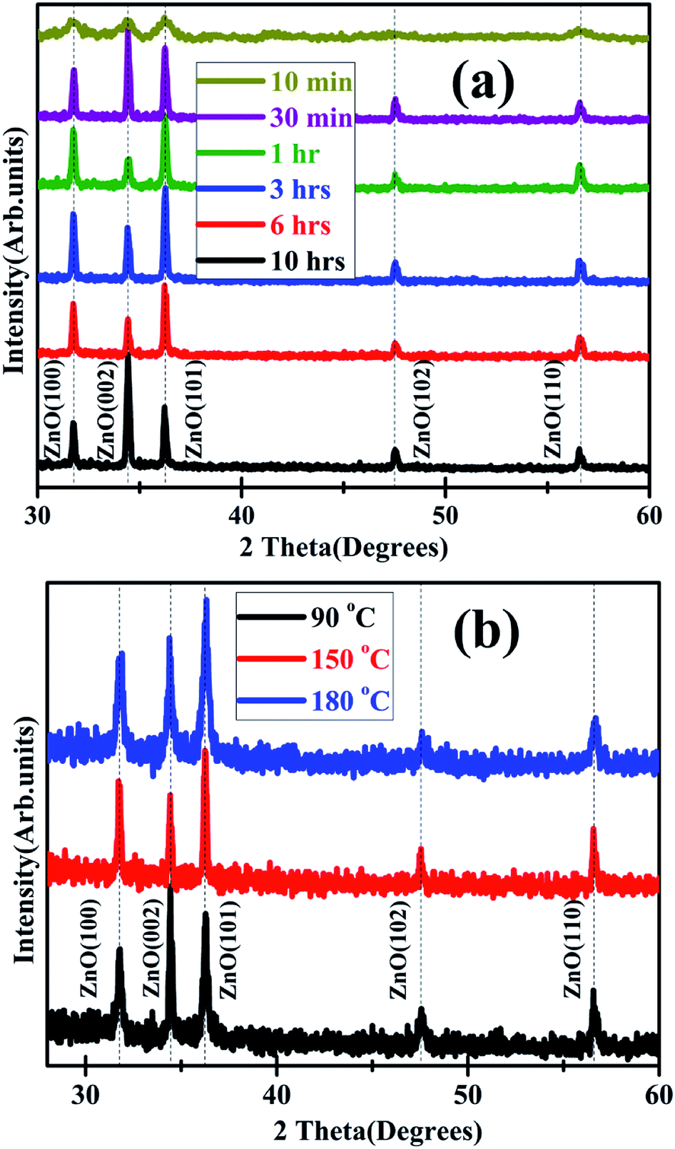 | ||
| Fig. 5 X-ray diffraction patterns of hydrothermally processed ZnO on 100 nm thickness ZnO film showing the effect of (a) increasing duration of processing at 120 °C and (b) increasing temperature at a fixed processing duration of 3 h. | ||
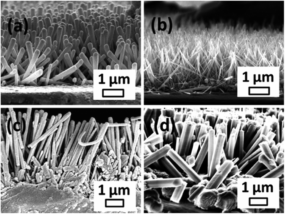 | ||
| Fig. 6 Scanning electron microscope images of hydrothermally processed ZnO for a duration of 3 h on 100 nm thickness ZnO films at (a) 90 °C, (b) 120 °C, (c) 150 °C and (d) 180 °C. | ||
These microstructural and structural evolutions of the ZnO nanowire arrays indicate that there is a “memory” effect i.e. the growth patterns are sensitive to the surface microstructure of the ZnO films on which they are grown. The surface of the 100 nm thin films comprises of 50–60 nm sized spherical particles and, there is increase in size of particles accompanied by a change in shape (from Fig. 1(a–d)) as the thickness is increased. The porosity also appears to increase with increase in thickness. As stated earlier, surface roughness as a contributing factor cannot be neglected. It would, thus, indicate that the surface of the 100 nm film provides more nucleation sites for the growth of nanorods/wires leading to the higher density and their lower diameter. The number of nucleation sites available for growth decrease with increase in thickness as a result of increase in grain size.20 It can, thus, be hypothesized that the interfacial free energy (i.e. at the interface between ZnO film and nanowires) is an important energy barrier that needs to be overcome for the growth of nanowires/rods. This can also be explained within the framework of Volmer–Weber mechanism, wherein the growth of nanowires on thin films is determined by strain energy minimization at the interface.27
At this point it is relevant to summarize the different conditions under which the ZnO homo-structures are grown and understand the possible mechanisms for the observed growth. The ZnO thin films of thickness 100–400 nm are prepared on glass substrates by thermal evaporation and subjected to post-deposition heat treatment at 400 °C for 2 h to ensure stoichiometry, crystallinity and remove metallic residues if any. FE-SEM studies indicate that the surface microstructure is profoundly thickness dependent. Subsequently, ZnO nanostructures are grown on these films by hydrothermal processing. The hydrothermal processing is carried out at different temperatures for a fixed duration and at a fixed temperature for different durations (all other conditions being the same). Three observations can be made (1) all the nanostructures are vertically oriented, independent of the conditions of processing and nature of underlying thin film surface (2) the dimensions and shapes are significantly dependent on the nature of the underlying ZnO thin film surface and (3) the nanowires are cylindrical in nature for hydrothermal durations of <3 h. Longer synthesis durations leads to the hexagonality of rods.
It is inferred, from these observations, that the hexagonal shape is the equilibrium shape for the rods, i.e. given favourable conditions it is most likely that the ZnO structures will only grow in the form of hexagonal rods, most likely due to the wurtzite structure of ZnO. This is consistent with earlier observations in literature.20
3.3 Photoluminescence, Raman spectroscopy, and optical properties of ZnO homo-structures
As in the case of microstructure and structure, initial studies are carried out on the 100 nm ZnO films to investigate their photoluminescence (PL) and Raman scattering behaviour. It is observed that the PL spectra of the ZnO thin films, shown in ESI Fig. S3(a),† display a prominent peak centred around 550 nm and a comparatively weaker peak centred around 380 nm. It is well documented that ZnO exhibits a near band-edge (NBE) PL peak at around 380 nm and defect related peak at approximately 550 nm. While the UV-NBE is attributed to the exciton–exciton scattering process from the n = 1 state to the exciton continuum state (P-line), the emission near 550 nm is generally assigned to oxygen vacancies (Vo).28Significantly, in the present case, UV-NBE is of much lower intensity than the visible-region emission. This would imply the existence of large volume of defects in the films in the form of oxygen vacancies or Zn interstitials. Another interesting aspect is the decrease in intensity of the defect related peak and corresponding increase in intensity of the UV-NBE with increase in thickness. This phenomenon is accompanied by a red-shift in both peak positions. The red-shift of the band edge emission has been attributed to the Burstein–Moss band filling effect or a band gap shrinkage due to charge transfer from un-reacted Zn to ZnO.
Raman spectra of these films displayed in ESI Fig. S3(b)† confirm these observations. There is a strong Raman band centred at 330 cm−1, which blue shifts (to 316 cm−1) and gets strengthened with the increase in thickness. The most intense band, expected from group theory considerations, centred around 437 cm−1 is very weak for the 100 nm thickness film. With increase in thickness the intensity of the peak increases and its existence is very evident for the 300 nm thickness film. The relative intensities of the high wavenumber to low wavenumber peaks increases with increase in thickness of the film. The low wavenumber peak at 330 cm−1 has been interpreted earlier as being a second order Raman scattering peak originating from multi-phonon scattering processes.29–31 This is ascribed to the E2(high)–E2(low) mode of ZnO, related to the zone boundary phonons, similar to GaN.31 The presence of these modes in un-doped ZnO thin films is unusual, since majority of the observations on this low wavenumber peak have been in the case of metal-doped ZnO. For example, in Mn doped ZnO there is clear evidence of the intensity of the peak increasing with increased dopant concentration.29 Multi-phonon processes are generally linked to the presence of disorder (such as defects and vacancies) in the material, which allows phonons of different symmetries to be scattered leading to the enhancement of their peak intensity. The blue-shifting of this peak can be attributed to increase in strain at the interface between the film and substrate due to heat treatment.32–35 Thus, the PL and Raman spectroscopy observations indicate the existence of defects in the thin films used to support the nanowire arrays.
The effect of these defects on the PL, Raman and optical spectra of the ZnO homo-structures are examined next. In all these cases, the ZnO film is of 100 nm thickness. The effect of increasing duration of hydrothermal processing at 120 °C on the PL spectra is shown in Fig. 7(a). As in the case of the thin film, the visible region peak centred around 550 nm is significantly more intense than the UV-NBE peak at 378(±2) nm after 10 min of HP. As the duration of processing increases there is an increase in the intensity of UV-NBE peak, while the intensity of the visible region peak (at 560 ± 2 nm) does not increase that significantly. After 10 h of HP, in addition to the peak at 378 nm, there are also two other peaks at 418 and 450 nm signifying the improved crystallinity of the nanowires as well as their hexagonal nature. This is also inferred from the large blue-shift of the defect related peak from 550 nm to 508 nm. Interestingly, when the temperature is increased from 90 °C to 180 °C at a fixed duration of 3 h (Fig. 7(b)), the intensity of the PL peak at 562(±2 nm) does not change very significantly upto 150 °C, but shows a decrease thereafter at 180 °C (Fig. 7(b)). The UV-NBE emission does not dominate over the visible PL, in this case implying that defects are still present and contributing to the PL spectra. This is also evident from the very intense peak at 650 nm in the case of the 90 °C HP sample.
 | ||
| Fig. 7 Photoluminescence spectra of ZnO homo-structures showing the effect of (a) varying duration of processing at 120 °C and (b) increasing temperature at a fixed processing duration of 3 h. | ||
Raman spectra displayed in Fig. 8(a) for the homo-structures as a function of increasing HP duration are very interesting due to their difference from the spectra of the thin films. In contrast to the thin films, there is complete absence of the second order Raman scattering peaks (at low wavenumbers) in the case of nanowires. The most intense peak is centred around 437 cm−1 characteristic of wurtzite ZnO, as stated earlier. This is also consistent with PL spectra discussed in Fig. 7(a and b), wherein the defect related peak decreases in intensity with increase in duration of HP. The appearance of very low intensity peaks at 569 and 579 cm−1 indicates presence of very small fraction of oxygen vacancies and other defects. Interestingly, at a fixed duration of HP with increasing temperature (Fig. 8(b)), the second order Raman peak at 330 cm−1 is very visible. In addition, the peak at 379 cm−1 assigned to the A1(TO) mode as a result of the displacement of Zn2+ and O2+ ions parallel to the c-axis is also observed. Both these modes indicate that increase in temperature for a fixed duration is not very conducive to remove the defects.
 | ||
| Fig. 8 Raman spectra of ZnO homo-structures showing the effect of (a) varying duration of processing at 120 °C and (b) increasing temperature at a fixed processing duration of 3 h. | ||
The optical transmission spectra, in Fig. 9(a), reveal that increase in duration of HP at a fixed temperature of 120 °C results in decrease in transmission as well as optical band gap. The 10 min HP sample has almost 60% transmission, which decreases to approximately 20% after 10 h of HP. The band gap, as a consequence of increased duration of HP, decreases from 3.4 eV to 2.6 eV. However, at a fixed HP duration of 3 h (Fig. 9(b)), the red-shift in band gap is much less (from 3.4 eV to 3.1 eV) in comparison to the change observed with increase in HP duration at a fixed temperature. Furthermore, the impact of increased temperature on optical transmission is very limited. All these homo-structures exhibit about 40% transmission in the visible and NIR regions.
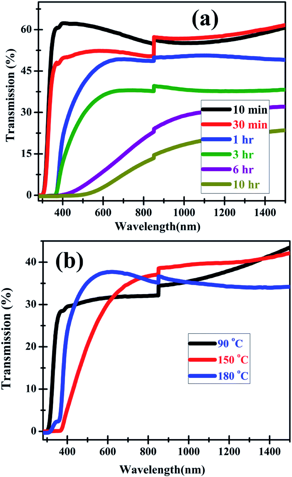 | ||
| Fig. 9 Optical transmission spectra of ZnO homo-structures showing the effect of (a) varying duration of processing at 120 °C and (b) increasing temperature at a fixed processing duration of 3 h. | ||
The picture that emerges from these studies is that the ZnO thin films show a large density of defects. This is attributed to the fact that thermal evaporation of high melting point materials such as ZnO induces non-stoichiometry in the deposited films.36 The presence of defects and the nature of the thin film surface play an important role in the PL and Raman spectra of the homo-structures. It is pertinent to recall that the PL emission at 380 nm is attributed to the recombination of free-exciton. The broad band emission from 400 nm to 600 nm revealed the radiative recombination of the photo-generated hole with the electrons that belonged to the singly ionized oxygen vacancies.28 The second broad peak features (peak position and peak intensity) of PL spectra gives the information of defect level distribution and its density. It is, thus, evident from the intensities and position of the PL spectra of the homo-structures that the defects in the nanowires and, as a consequence, the emission (wavelength and intensity) from them is strongly dependent on the defects in the underlying thin films. It could be inferred that the defects propagate in to the nanowires upto a length of 1–2 microns. As the length of the nanowires increase beyond this value, the effect of the defects on photoluminescence decreases and the intensity of the UV-NBE increases. This is very interesting for LED applications based on such homo-junctions as it provides the possibility of defect-controlled emission.9–16
4. Conclusions
In summary, the growth of ZnO thin film-nanowire homo-junctions is reported. The thin films are grown by thermal evaporation on glass substrates followed by post-deposition heat treatment at 400 °C for 2 h. These films exhibit thickness dependent morphology ranging from spherical particles to flakes. X-ray diffraction studies indicate the films are polycrystalline in nature. Photoluminescence and Raman spectroscopy studies show that the films have a large density of defects. The optical band gap is of the order of 3.4 eV. Nanowires are grown on top of the films using hydrothermal processing from a zinc acetate precursor. The dimensions of nanowires are strongly dependent on the temperature (90 °C to 180 °C) and duration of synthesis (10 min to 10 h) apart from the morphology of the films. Interestingly, the defect related emission is suppressed in the nanowires as evidenced from the photoluminescence spectra, which is confirmed by Raman spectra. The current study indicates that emission from the homo-structures can be controlled by controlling dimensions and defects in the nanowires.Conflicts of interest
There are no conflicts to declare.Acknowledgements
Y. Rajesh acknowledges a NFHE PhD fellowship awarded by UGC. S. K. Padhi acknowledges DRDO financial support through ACRHEM, University of Hyderabad. Center for Nanotechnology and School of Physics, University of Hyderabad, India are acknowledged for facilities. The support of DST-PURSE, UGC-DRS, UGC-NRC programmes is also acknowledged.References
- Z. L. Wang, J. Phys.: Condens. Matter, 2004, 16, R829 CrossRef CAS.
- S. Singh, P. Thiyagarajan, K. M. Kant, D. Anita, S. Thirupathiah, N. Rama, B. Tiwari, M. Kottaisamy and M. S. R. Rao, J. Phys. D: Appl. Phys., 2007, 40, 6312 CrossRef CAS.
- M. Law, L. E. Greene, J. C. Johnson, R. Saykally and P. D. Yang, Nat. Mater., 2005, 4, 455 CrossRef CAS PubMed.
- Z. R. Tian, J. A. Voigt, J. Liu, B. Mckenzie, M. J. Mc Dermott, M. A. Rodriguez, H. Kingishi and H. Xu, Nat. Mater., 2003, 2, 821 CrossRef CAS PubMed.
- X. Wang, C. J. Summers and Z. L. Wang, Nano Lett., 2004, 4, 423 CrossRef CAS PubMed.
- S. Santra, P. K. Guha, S. Z. Ali, P. Hiralal, H. E. Unalan, J. A. Covington, G. A. Amaratunga, W. I. Milne, J. W. Gardner and F. Udrea, Sens. Actuators, B, 2010, 146, 559 CrossRef CAS.
- U. P. Shaik, S. Hamad, M. A. Mohiddon, S. V. Rao and M. G. Krishna, J. Appl. Phys., 2016, 119, 093103 CrossRef.
- U. P. Shaik, S. Kshirsagar, M. G. Krishna, S. P. Tewari, D. D. Purkayastha and V. Madhurima, Mater. Lett., 2012, 75, 51 CrossRef CAS.
- F. Rahman, Opt. Eng., 2019, 58, 010901 CAS.
- H. Sun, Q. Zhang, J. Zhang, T. Deng and J. Wu, Appl. Phys. B, 2008, 90, 543 CrossRef CAS.
- M. Su, T. Zhang, J. Su, Z. Wang, Y. Hu, Y. Gao, H. Gu and X. Zhang, Opt. Express, 2019, 27, A1207 CrossRef CAS PubMed.
- V. Kampylafka, A. Kostopoulos, M. Modreanu, M. Schmidt, E. Gagaoudakis, K. Tsagaraki, V. Kontomitrou, G. Konstantinidis, G. Deligeorgis, G. Kiriakidis and E. Aperathitis, J. Materiomics, 2019, 5, 428 CrossRef.
- S. Baek, Y. Porte, Y. C. Kim and J.-M. Myoung, J. Mater. Chem. C, 2017, 5, 9479 RSC.
- Y. Geng, K. Jeronimo, M. A. B. C Mahzan, P. Lomax, E. Mastropaolo and R. Cheung, Nanoscale Adv., 2020 10.1039/c9na00553f.
- D.-K. Kwon, Y. Porte and J.-M. Myoung, J. Phys. Chem. C, 2018, 122, 11993–12001 CrossRef CAS.
- G. Wang, S. Chu, N. Zhan, Y. Lin, L. Chernyak and J. Liu, Appl. Phys. Lett., 2011, 98, 041107 CrossRef.
- S. Baruah and J. Dutta, Sci. Technol. Adv. Mater., 2009, 10, 013001 CrossRef PubMed.
- J. A. Darr, J. Zhang, N. M. Makwana and X. Weng, Chem. Rev., 2017, 117, 11125 CrossRef CAS PubMed.
- W. Shi, S. Song and H. Zhang, Chem. Soc. Rev., 2013, 42, 5714 RSC.
- T. Demes, C. Ternon, D. Riassetto, V. Stambouli and M. Langlet, J. Mater. Sci., 2016, 51, 10652 CrossRef CAS.
- S. Vyas, P. Giri and S. Singh, J. Electron. Mater., 2015, 44, 3401 CrossRef CAS.
- Y. Z. Liu, Y. C. Liu, D. Z. Shen, G. Z. Zhong, X. W. Fan, X. G. Kong, R. Mu and D. O. Henderson, Solid State Commun., 2002, 121, 531 CrossRef CAS.
- M. C. Akgun, Y. E. Kalay and H. E. Unalan, J. Mater. Res., 2012, 27, 1445 CrossRef CAS.
- C. P. Tsangarides, H. Ma and A. Nathan, Nanoscale, 2016, 8, 11760 RSC.
- A. Sugunan, H. C. Warad, M. Boman and J. Dutta, J. Sol-Gel Sci. Technol., 2006, 39, 49 CrossRef CAS.
- C. Lausecker, B. Salem, X. Baillin, H. Roussel, E. Sarigiannidou, F. Bassani, E. Appert, S. Labau and V. Consonni, Nanotechnology, 2019, 30, 345601 CrossRef CAS PubMed.
- S. J. Park, J. Qiu, W. He, W. Namgung, K. Wan, Y. Kim, J.-H. Lee, Y.-H. Hwang and H.-K. Kim, J. Nanosci. Nanotechnol., 2009, 9, 6993 CAS.
- S. D. Kshirsagar, U. P. Shaik, M. Ghanashyam Krishna and S. P. Tewari, J. Lumin., 2013, 136, 26 CrossRef CAS.
- V. Strelchuk, O. Kolomys, S. Rarata, P. Lytvyn, O. Khyzhun, C. O. Chey, O. Nur and M. Willander, Nanoscale Res. Lett., 2017, 12, 351 CrossRef CAS PubMed.
- H. K. Yadav, K. Sreenivas, V. Gupta and R. S. Katiyar, J. Raman Spectrosc., 2009, 40, 381 CrossRef CAS.
- S. Guo, Z. Du and S. Dai, Phys. Status Solidi B, 2009, 246, 2329 CrossRef CAS.
- H. Siegle, G. Kaczmarczyk, L. Filippidis, A. P. Litvinchuk, A. Hoffmann and C. Thomsen, Phys. Rev. B, 1997, 55, 7000 CrossRef CAS.
- Y. Huang, M. Liu, Z. Li, Y. Zeng and S. Liu, Mater. Sci. Eng., B, 2003, 97, 111 CrossRef.
- S. B. Yahia, L. Znaidi, A. Kanaev and J. P. Petitet, Spectrochim. Acta, Part A, 2005, 71, 1234 CrossRef PubMed.
- L. Wang, Y. Pu, Y. F. Chen, C. L. Mo, W. Q. Fang, C. B. Xiong, J. N. Dai and F. Y. Jiang, J. Cryst. Growth, 2005, 284, 459 CrossRef CAS.
- D. Gogova, L.-K. Thomas and B. Camin, Thin Solid Films, 2009, 517, 3326 CrossRef CAS.
Footnote |
| † Electronic supplementary information (ESI) available. See DOI: 10.1039/d0ra04524a |
| This journal is © The Royal Society of Chemistry 2020 |