
 Open Access Article
 This Open Access Article is licensed under a Creative Commons Attribution-Non Commercial 3.0 Unported Licence
Influence of gamma-ray irradiation and post-annealing studies on pentacene films: the anisotropic effects on structural and electronic properties†
Aswin kumar Anbalagana,
Chun-Yu Jaob,
Maliya Syabriyanacd,
Chen-Lin Fana,
Shivam Guptad,
Mayur Chaudharyd,
Yu-Lun Chueh d,
Nyan-Hwa Taid and
Chih-Hao Lee*ab
d,
Nyan-Hwa Taid and
Chih-Hao Lee*ab
aDepartment of Engineering and System Science, National Tsing Hua University, Hsinchu, 30013, Taiwan. E-mail: chlee@mx.nthu.edu.tw
bInstitute of Nuclear Engineering and Science, National Tsing Hua University, Hsinchu, 30013, Taiwan
cDepartment of Chemical Engineering, Universitas Serambi Mekkah, Banda Aceh, 23245, Indonesia
dDepartment of Material Science and Engineering, National Tsing Hua University, Hsinchu, 30013, Taiwan
First published on 4th June 2020
Abstract
In this work, γ-ray irradiation effects on pentacene thin films are investigated in terms of the change in the crystallinity, and electronic structure as well as chemical states of the film. The pentacene films are γ-irradiated up to 3 kGy and then characterized using synchrotron X-ray diffraction, near edge X-ray absorption fine structure (NEXAFS) and X-ray photoelectron spectroscopy. We found that γ-ray irradiation creates defects, resulting in a decrease of X-ray diffraction intensity both in the plane normal and in-plane directions. From angle dependent NEXAFS; the transition of C 1s to π* orbital for irradiated samples increases; suggesting that the unoccupied π* states enhance due to defects or radical formation in pentacene thin films. Additionally, the in-plane resistivity shows a decreasing trend of resistance after irradiation. This trend of increase in conductivity is also consistent with C 1s to π transition, which manifests the increase in carrier concentration. Hall effect measurements further confirmed the increase in carrier concentration as a function of dose; however, the mobility of the sample decreases as the dose rate increases due to the defects created. By post-irradiation annealing, the thin film phase diffraction intensity can be recovered. Altogether, the anisotropic studies on pentacene films disclosed that the irradiation leads to defect formation along in-plane and plane normal directions. Overall, these results suggest that pentacene is one of the robust organic electronic materials; whose structure remains mostly intact even after irradiation up to a dose of 3 kGy.
Introduction
Organic semiconductors have emerged as a vibrant field of research during the past decades in wearable and flexible electronics owing to their superiorities of flexibility, and being easy to fabricate in large area.1 The fabrication of low cost large area radiation monitors based on small molecule semiconductors has become crucial to attain high performance organic electronic devices.2–4 Especially, it can play an important role in the high level rad-waste monitoring area during the decommissioning of nuclear power plants, and in space related applications. Pentacene is commonly employed in organic thin film transistors and organic field effect transistors because of its high mobility.5 Pentacene is a polycyclic aromatic hydrocarbon organic semiconductor.6,7 For decades, many groups have studied various organic based materials under different radiations such as IR, X-ray, proton, gamma, etc. and they noticed an increase in the conductivity. At the same time, they proposed that the organic based materials can be used as an active sensing layer in real applications such as sensors.8–13 Furthermore, studies related to the change in electronic and structural properties with respect to dose are essential for radiation sensor applications.Previously, some research groups have studied the changes in the chemical properties of pentacene based thin films by angular dependent near edge X-ray absorption fine structure (NEXAFS) technique and analyzed the orientation of the molecules with different combinations of layers.14–18 However, the key technology in tuning molecular packing of organic semiconductors on polymeric insulators is still deficient, but its importance along with different dielectric configurations were discussed previously.19–22
Yet, the mechanism, neither due to the change in phase transition nor the electronic structure owing to γ-ray irradiation, has not been studied in detail. Until now, most reports provide an overview of radiation effects on the electronic transport properties of pentacene thin film.23–26 Moreover, the scope of our work is unique, since we analyzed the effects of γ-irradiation at different dose levels among π and σ bonds existing in the molecule. Pentacene thin film is a layered structured material and anisotropic studies on such type of material lead to a better understanding of the irradiation effects on the molecular level along in-plane and plane normal directions. To understand whether there will be any structural modification in the pentacene thin films owing to γ-ray irradiation, sample characteristics such as crystallinity, morphology, electronic & chemical structure change were studied anisotropically. Finally, the post-annealing treatment was studied to understand the possibility of recovery of films after irradiation, and its results were discussed below.
Experimental
Pentacene of 99% purity was purchased from Sigma-Aldrich and it was used without further purification. Silicon wafers of 1 cm × 1 cm with a thermally grown oxide layer of 300 nm were employed as substrates. The substrates were solvent cleaned using acetone and rinsed further with ethanol, followed by deionized water for 5 min under the ultra-sonication process and finally dried by N2 stream. Pentacene thin films of around 80–100 nm were deposited on the Si substrates using thermal evaporation technique at a pressure of about 2 × 10⁻⁵ torr.To measure the change in resistivity anisotropically, a simple semiconductor device was fabricated. The source and drain electrodes were then fabricated by depositing copper (Cu) electrodes of 60 nm on the top of pentacene thin films through shadow mask forming Cu/pentacene/SiO2/Si structure. The devices have a channel width of 8000 μm and a channel length of 200 μm. The carrier concentration and mobility of the samples were determined by Hall effect measurements using ECOPIA HMS-5000. Four copper contacts (60 nm) as electrodes were deposited by sputtering with a channel length of about 400 μm. γ-Ray radiation exposures were performed using 29 kCi 60Co source with the energies of 1.173 MeV and 1.332 MeV at Radioisotope Laboratory Facility of National Tsing Hua University. Different doses of samples were obtained by varying the exposure time at a dose rate of 1 kGy h−1 to attain the total dose of 400 Gy and 3000 Gy.
The thickness and surface morphology of the thin films were determined by using scanning electron microscope (JEOL, JSM, 7610F) and surface profiler (Veeco, Dektak 150). Atomic Force Microscopy (AFM) was utilized to study morphology and the roughness of the samples before and after irradiation by tapping mode. Raman spectroscopy was performed at room temperature by using 633 nm excitation laser (HORIBA HR800). Synchrotron X-ray diffraction (XRD) measurements were carried at the end stations of beamline 13A, 07A & 17B27 at National Synchrotron Radiation Research Center (NSRRC) facility, Taiwan. The plane normal XRD was performed to study the change in the crystallinity as well as the ordering of the thin films; whereas to understand the orientations of the molecular packing structure along the in-plane directions, in-plane Grazing Incidence X-ray diffraction (GIXD) technique using 8 circle diffractometer was performed. The electronic structure of carbon K-edge for pentacene thin films before and after γ-ray irradiation was studied at BL-20A in NSRRC by utilizing total electron yield (TEY-XAS) mode. To examine the variation in the chemical surface states of the films, X-ray Photoelectron Spectroscopy (XPS) was carried out at BL-24A of NSRRC facility. Resistance measurement was obtained from the I–V curves using Keithley 4200 Semiconductor Characterization System at room temperature. To study the recovery of the thin film phase after irradiation, post-annealing treatment was carried out at various temperatures in vacuum at a pressure of about 1.2 × 10⁻⁵ torr for 1 h. Later, the samples were allowed to cool down slowly until they reach room temperature.
Results and discussion
To scrutinize whether the γ-ray radiations altered the structure and crystallinity of pentacene thin films, we analyzed the XRD results of pentacene thin films before and after irradiations. Fig. 1(a) shows that the observed XRD pattern of pentacene thin films, which is consistent with the earlier reported work by T. S. Huang et al.,28 confirming the co-existence of two phases in pentacene thin films. Two phases existing in pentacene films are marked in Fig. 1(a) as subscript T and B, where T stands for thin film phase and B for bulk phase. Predominantly, we can observe from Fig. 1(b) that the (001)T peak intensity of the pristine sample is higher when compared to the irradiated samples at various doses. This change in intensity of (001)T is observed to be lesser than 10% with respect to pristine sample. This degradation of intensity might be due to the irradiation induced defects created in the sample. The intensity values, peak positions, and the corresponding parameters for the pristine and irradiated samples are summarized in Table 1. It can be observed that the coherent length and Debye–Waller factor values calculated are within 3% of uncertainty, which reveals the main structure of pentacene is not radiation damaged with a dose up to 3 kGy. This radiation tolerance could be due to the nature of aromatic rings existing in pentacene thin films.11 | ||
| Fig. 1 (a) Normalized intensity vs. 2 theta of plane normal XRD of pentacene thin films at various doses and (b) enlarged view of pentacene (001)T film at various doses all measured at λ = 1.5406 Å. | ||
| Dose | % of intensity degradation | d (Å) | Tilt angle (°) |
|---|---|---|---|
| Pristine | 0 | 15.34 | 16.63 |
| 400 Gy | 2.27 | 15.37 | 16.26 |
| 3000 Gy | 8.03 | 15.4 | 15.87 |
Fig. 2(a) and (b) show the in-plane X-ray diffraction pattern measured at a grazing angle of 0.15°. The (110) diffraction represents the distance between the pentacene planes held together by π–π interactions, which is consistent with previous reports,29 and the strong diffraction peaks tend to assume a herringbone structure.30 Unlike the preferred orientation of (001)T in the plane normal direction, the rocking curve of (110)T reveals a powder form in the surface plane with a grain size of about 14.2 nm, deduced from Scherrer's formula. The in-plane GIXD results reveal a decrease in the integrated intensity after irradiation, which is similar to our plane normal data. This degradation of XRD results suggests that the arrangements of atoms are well ordered before irradiation and some defects are formed in the molecular packing after exposure to 3 kGy dose, resulting in a reduced diffraction intensity. Herringbone angle of pristine sample is around 52.6°, which is similar to the report of other groups,31,32 however, it reduces to 50.9° after irradiation of 3 kGy. This herringbone angle shift can also be seen in the work of Meyenburg et al. in which the angle shift was due to heating of the pentacene molecules at different temperatures.33 In our case, the herringbone angle shift has occurred due to the defects or radicals created in the molecule after irradiation.
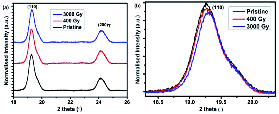 | ||
| Fig. 2 (a) In-plane (grazing incidence = 0.15°) of pentacene based thin films at various doses and (b) enlarged view of pentacene (110) in-plane peak at various doses measured at λ = 1.54981 Å. | ||
The morphology and the roughness were investigated for the thin films before and after irradiation using AFM and SEM, as shown in Fig. S1 and S2,† respectively. No noticeable change in the physical appearance and morphology can be observed for the samples exposed to various doses. The average domain size from AFM is around 18.8 nm and the coherent length of the thin film is about 14.2 nm from the GIXD data. The average in-plane domain size and coherent length before and after irradiation did not change significantly. Raman spectra of pentacene thin films before and after irradiation were carried out at room temperature in the range of 1000–1700 cm−1, as shown in Fig. S3.† The changes in the Raman spectra due to the molecular vibrations across C–H bending and C–C stretching in case of pristine and irradiated samples are deemed to be within the statistical error limit. These results also confirm that the structure of the pentacene molecules remains intact after irradiating to a dose of up to 3 kGy.
To determine the electronic structure of the pentacene molecule at different orientations, polarized angular dependent XAS studies was carried out at BL 20A of NSRRC facility. It can be observed that the intensity of C 1s to π* transition changes with respect to the incident photon angle, which confirms that the pentacene molecule is grown in the form of a layered structure, resulting in the orthogonality fashion existing between π and σ orientations.14,18,34 C 1s NEXAFS spectra for pentacene film grown on SiO2/Si surfaces were performed at various incidence angles. Herein, 90° and 30° represent the angle between the surface of the sample and the direction of the polarization vector of light, which were shown in Fig. 3(a) and (b), respectively. In the C 1s NEXAFS, different types of resonance exist. The resonances in between 283–287 eV corresponds to the transition of core electrons into unoccupied π* state of the sp2-hybridized carbon atoms, between 287–291 eV into C–H*/Rydberg states and between 291–315 eV into σ* states.34–37 Furthermore, in-plane (90°) NEXAFS has resulted in a higher white line intensity of π* states in the 3 kGy irradiated sample. This experimental result suggests a relatively higher amount of unoccupied valence orbital for 3 kGy irradiated samples, whereas the attenuated intensity in the pristine sample is attributed to almost completely filled valence orbital.
 | ||
| Fig. 3 Normalized XAS absorption spectra for C 1s at various γ-ray doses measured at (a) in-plane (90°) and (b) plane normal (30°); the inset shows the extended view of π & σ orientation, whereas 90° & 30° indicate the angle between the surface of the sample and the direction of the polarization vector of light. | ||
The post edge regions around 291–315 eV are responsible for σ transitions where the changes before and after irradiations are within the error limit because σ bonds are stronger in comparison to the π bonds. In addition, it can be observed from Fig. 3(b) that the spectra follow a similar trend in which the 3 kGy irradiated sample has more unoccupied π* states in comparison to the pristine sample. However, due to the anisotropic nature of the sample, it can be seen that σ transitions dominates over π transitions. Overall, from the NEXAFS data, it could be concluded that the increase in unoccupied π* states lead to the change in the white line intensity due to the defects or radicals created after γ-ray irradiation. Furthermore, it can be seen that the change in density of states along in-plane directions leads to an increase in the conductivity of the film. This is mainly because the electron transport in pentacene molecule occurs predominantly along π–π orientation.
XPS was carried out to determine whether any changes occurred in the chemical states of the pentacene films before and after γ-ray exposure. Fig. S4† shows the XPS spectrum of the C 1s peak, whose binding energy lies around 284.8 eV corresponding to the sp2 hybridized carbon atoms present in the pentacene molecule. No significant change or shift in the binding energy was observed, which further suggests that the pentacene structure remains intact even after γ-ray exposure of 3 kGy.
The phenomena of radiation generated carrier concentration can facilitate the use of organic semiconductors as sensors in various high radiation areas. Therefore, a simple resistor was fabricated to study these effects anisotropically and understand the change in resistivity along in-plane and plane normal directions upon exposure to ionizing radiation. Fig. 4(a) shows a simple pentacene based organic resistor fabricated on the Cu electrodes to measure the change in resistance across the in-plane direction (i.e. along the π–π interaction of the molecule). To correlate the effects due to γ-ray irradiation along the plane normal direction, a vertical based device was fabricated, as shown in Fig. 4(b). As the dose level increased to 3 kGy, the resistivity along in-plane direction decreases with respect to the pristine sample, as can be seen from Fig. 4(c). The resistivity decreases from 20 × 104 Ω cm to 2.4 × 10⁴ Ω cm after exposure to 3 kGy, confirming the increase in conductivity of the thin films upon γ-ray exposure. Since the in-plane orientation of the pentacene molecules is bounded by π–π interaction, the decrease in the resistivity of the films after irradiation attributes to the enhanced electron transport across the in-plane direction. Whereas, across the plane normal direction, the resistivity of the pristine sample is around 6.8 × 10⁷ Ω cm, which is three orders of magnitude higher than the in-plane resistivity. The high resistivity in the plane normal direction reveals the existence of van der Waals force between the layered structure of pentacene thin films, which further confirms that electron transport mainly occurs through π–π interaction of the sample. Meanwhile, the plane normal resistance after irradiation remains unaffected, which is totally different from the in-plane resistivity data. This could be due to the weak van der Waals force along the vertical direction.
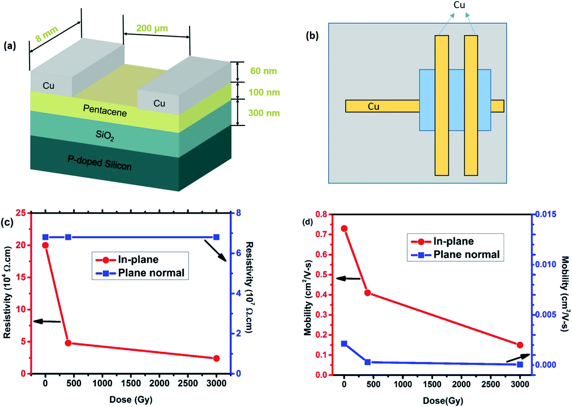 | ||
| Fig. 4 (a) Schematic diagram of bottom-gate top-contact configuration; (b) vertical configuration of pentacene based resistor device; (c) change in the resistivity along in-plane and plane normal orientation as a function of dose and (d) change in mobility along in-plane and plane normal orientation as a function of dose for pentacene thin film. | ||
To further illustrate the details of resistivity, Hall mobility measurement was performed. Fig. S5† shows a schematic pattern fabricated for Hall effect measurement. The Hall effect measurement is more crucial to know the carrier concentration change in the pentacene films along plane normal and in-plane directions. The previously discussed NEXAFS data shows that the density of the unoccupied states increases after γ-ray irradiation, which is possible due to some intermediate energy states created after γ-ray irradiation. This led to boost up the carrier transport, which indicates the increase of carrier concentration of the irradiated samples due to ions and free radicals created. The carrier mobility on different orientations of the thin film can be calculated from σ = enμ, where σ stands for conductivity, e is the unit charge, n is the carrier concentration and μ is the carrier mobility. It can be seen from Fig. 4(d) that the in-plane mobility decreases as a function of dose. However, along plane normal direction, no significant change in mobility was observed. Such a phenomenon of the decrease in mobility might result from the anisotropic structural disorders that are created after irradiation. This result is consistent with the other reported works, in which mobility decreased after irradiation.11,24,26 In this work, the resistivity decreases (Fig. 4(c)) together with the mobility (Fig. 4(d)) as a function of dose, which implies an increase of carrier concentration after γ-ray irradiation. Additionally, this effect occurs only along the in-plane π–π orientation.
Table 2 lists a comparison of mobility values obtained from other reported works with different gate dielectric materials as well as using different methods utilized for mobility measurement. Hall-effect mobility is usually much higher than the mobility derived from the transfer characteristics of field-effect method.38 In case of the field-effect method, this change in the mobility value is obvious because the charge carrier transport is known to occur within the first few nanometers of the thin film adjacent to the dielectric layer.39 Carrier traps at interface always give rise to the reduction of mobility value, while Hall measurement gives higher mobility values for thicker films.
| Gate dielectric material | Measurement method | Carrier mobility (cm2 V−1 s−1) | Ref. |
|---|---|---|---|
| SiO2 | Field-effect | 0.4 | H. Klauk et al.43 |
| SiO2 | Field-effect | 0.45 | R. Ruiz et al.44 |
| Al2O3 | Field-effect | 0.45 | A. A. Gunther et al.45 |
| SiO2 | Field-effect | 1.0 | L. Cai et al.26 |
| SiO2 | Field-effect | 1.5 | Y. Y. Lin et al.46 |
| Al2O3 | Field-effect | 2.4 | J. H. Schön et al.47 |
| Polyimide | Hall-effect | 0.4 | T. Sekitani et al.48 |
| Glass | Hall-effect | 3.0 | Y. J. Lin et al.49 |
| Glass | Hall-effect | 2.42 | H. Y. Tsao et al.50 |
| SiO2 | Hall-effect | 0.73 (pristine), 0.41 (400 Gy), 0.15 (3000 Gy) | This work* |
To understand the possibility of the recovery of the pentacene films after irradiation and illustrating its usage for reversible dosimetry applications, post-annealing studies were carried out.
Guo et al.40 reported that post-annealing led to a decrease of the XRD intensity of the thin film phase of pristine samples at various temperatures. They reported that the post-annealing treatments of pentacene films at 45, 50 and 70 °C led to the decrease in the ordering of the molecules of the pristine sample. Besides the decrease in diffraction intensity of pristine sample, we found that the reduction of thin film phase intensity upon the post-annealing treatment is correlated with the strain relaxation effect.
This result suggests the conversion of thin film phase into the bulk phase of the pentacene thin films, as shown in Fig. 5(a), which is consistent with the work of S. G. Jeong et al.41 Whereas in the case of irradiated samples, the post-annealing situation could be different. Since the pentacene thin film after irradiation is less stable, the disordered molecule perhaps could be vibrating in all orientations to release energy due to induced radiation effect. Therefore, pentacene molecules are easier to realign in well-orderly fashion by the post-annealing treatment for those irradiated samples. Post-annealing treatment at 80 °C for 1 h in vacuum for those irradiated pentacene films shows an increase in the Bragg peak intensity of the thin film phase, as shown in Fig. 5(b) and (c). Additionally, it can also be seen that the diffraction intensity recovery in the case of 400 Gy sample is higher in comparison to the 3 kGy sample. It may be because the defects created in 400 Gy samples are at lower concentrations and the defected radicals do not interact with each other. Whereas the sample irradiated at 3 kGy dose consists of highly interacted defects or permanent damage in the crystal structure, resulting in a difficulty to recover or re-ordering to the same fashion like 400 Gy samples.
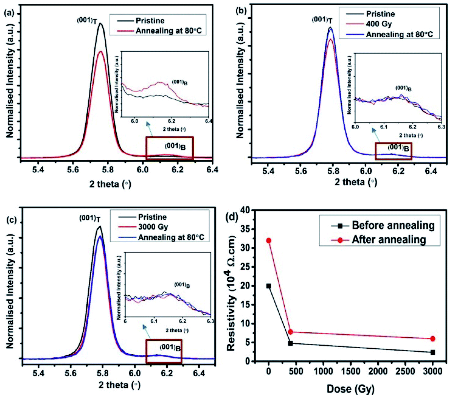 | ||
| Fig. 5 XRD spectra of (a) pristine, (b) 400 Gy, (c) 3000 Gy of irradiated pentacene film and (d) resistance measurement before and after annealing. The inset shows the enlarged view of (001)B peak. | ||
Along with the XRD measurements after the post-annealing treatment, resistance measurements have been carried out to check the possibility of the recovery of the film. It can be seen from Fig. 5(d) that annealing at 80 °C leads to the increase in resistivity, which could result from either carrier mobility decrease or carrier concentration decrease. In a non-irradiated sample, the decrease in mobility is usually due to a higher degree of mixed phases (bulk and thin film phases) co-existing in the pentacene thin film. A conversion of thin film phase into the bulk phase gives rise to a higher resistance, as reported by T. Ji et al.42 This phenomenon seems consistent with our post-annealing XRD results of pristine samples. However, the post-annealing treatment leads to the increase in the resistivity in case of irradiated samples. This could be due to the recombination of the radicals that further decrease the carrier concentration because the XRD bulk phase intensity did not increase after annealing, as shown in Fig. 5(b) and (c).
In summary, the conductivity change of the pentacene thin films after irradiation suggests that irradiation can be used as a potential tool for the detection of ionizing radiation.
Conclusion
In this work, we studied the effects of 60Co γ-ray irradiation on the crystallinity, electronic structure, chemical states, and electrical properties of pentacene thin films anisotropically. From the XRD results, across the plane normal and in-plane directions, confirmed that the structure of pentacene remains robust. About 10% of integrated diffraction intensity dropped after 3 kGy of γ-ray irradiation. NEXAFS results revealed that the C 1s transition to unoccupied valence states of π orientation is enhanced after irradiation along both in-plane and plane normal directions. In σ orientation, the change is within the statistical limit. On the other hand, the resistivity study of pentacene thin film under γ-ray exposure confirmed an increase in the conductivity of the device. This result is also consistent with C 1s → π transition from NEXAFS result; that manifests the increase in carrier concentration along the in-plane direction (i.e. along π–π orientation), which is responsible for the electron transport in the pentacene molecule. Mobility of the samples decreases as a function of dose along the in-plane direction, confirming the defects or radicals created in the samples owing to γ-ray irradiation. Furthermore, the post-annealing treatment revealed the recovery of the thin film phase diffraction intensity after γ-ray exposure. Altogether from the obtained results, it can be concluded that pentacene could serve as a tool for radiation sensing applications over a large area due to its radiation tolerance capacity.Conflicts of interest
The authors declare no conflict of interest.Acknowledgements
This work was supported by the Ministry of Science and Technology of Taiwan under the contract number of MOST-105-2112-M-007-023. The γ-ray irradiation facility at National Tsing Hua University is acknowledged. The beam time offered by the NSRRC is also highly appreciated.References
- Q. Liu, G. Lu, Y. J. Xiao, Y. W. Ge and B. Wang, Thin Solid Films, 2017, 626, 209–213 CrossRef CAS.
- J. H. Chen, M. Shao, K. Xiao, Z. R. He, D. W. Li, B. S. Lokitz, D. K. Hensley, S. M. Kilbey, J. E. Anthony, J. K. Keum, A. J. Rondinone, W. Y. Lee, S. Y. Hong and Z. A. Bao, Chem. Mater., 2013, 25, 4378–4386 CrossRef CAS.
- Z. R. He, S. Shaik, S. Bi, J. H. Chen and D. W. Li, Appl. Phys. Lett., 2015, 106, 5 Search PubMed.
- K. Asare-Yeboah, S. Bi, Z. R. He and D. W. Li, Org. Electron., 2016, 32, 195–199 CrossRef CAS.
- I. P. M. Bouchoms, W. A. Schoonveld, J. Vrijmoeth and T. M. Klapwijk, Synth. Met., 1999, 104, 175–178 CrossRef CAS.
- J. L. Zhenan Bao, Organic Field-Effect Transistors, 1st edn, 2007 Search PubMed.
- C. D. Dimitrakopoulos and P. R. L. Malenfant, Adv. Mater., 2002, 14, 99–117 CrossRef CAS.
- H. N. Raval, S. P. Tiwari, R. R. Navan and V. R. Rao, Appl. Phys. Lett., 2009, 94, 3 CrossRef.
- L. Basirico, A. F. Basile, P. Cosseddu, S. Gerardin, T. Cramer, M. Bagatin, A. Ciavatti, A. Paccagnella, A. Bonfiglio and B. Fraboni, ACS Appl. Mater. Interfaces, 2017, 9, 35150–35158 CrossRef CAS PubMed.
- J. J. Kim, J. M. Ha, H. M. Lee, H. S. Raza, J. W. Park and S. O. Cho, ACS Appl. Mater. Interfaces, 2016, 8, 19192–19196 CrossRef CAS PubMed.
- T. Y. Kim, J. Jang, K. Cho, Y. Song, W. Park, J. Park, J. K. Kim, W. K. Hong and T. Lee, Org. Electron., 2015, 27, 240–246 CrossRef CAS.
- A. Neuhold, J. Novak, H. G. Flesch, A. Moser, T. Djuric, L. Grodd, S. Grigorian, U. Pietsch and R. Resel, Nuclear Instruments & Methods in Physics Research Section B-Beam Interactions with Materials and Atoms, 2012, 284, 64–68 Search PubMed.
- C. H. Wang, S. W. Chen and J. Hwang, Appl. Phys. Lett., 2009, 95, 3 Search PubMed.
- T. Schwieger, X. Liu, D. Olligs, M. Knupfer and T. Schmidt, J. Appl. Phys., 2004, 96, 5596–5600 CrossRef CAS.
- Y. Natsume, T. Kohno, T. Minakata, T. Konishi, E. M. Gullikson and Y. Muramatsu, J. Phys. Chem. A, 2012, 116, 1527–1531 CrossRef CAS PubMed.
- H. K. Lee, J. H. Han, K. J. Kim, T. H. Kang and B. Kim, Surf. Sci., 2007, 601, 1456–1460 CrossRef CAS.
- A. Manz, A. A. Hauke and G. Witte, J. Phys. Chem. C, 2018, 122, 2165–2172 CrossRef.
- S. Kowarik, K. Broch, A. Hinderhofer, A. Schwartzberg, J. O. Osso, D. Kilcoyne, F. Schreiber and S. R. Leone, J. Phys. Chem. C, 2010, 114, 13061–13067 CrossRef CAS.
- D. Y. Ji, Y. D. Wang, L. F. Chi and H. Fuchs, Adv. Funct. Mater., 2015, 25, 3855–3859 CrossRef CAS.
- M. Halik, H. Klauk, U. Zschieschang, G. Schmid, C. Dehm, M. Schutz, S. Maisch, F. Effenberger, M. Brunnbauer and F. Stellacci, Nature, 2004, 431, 963–966 CrossRef CAS PubMed.
- J. Liu, H. T. Zhang, H. L. Dong, L. Q. Meng, L. F. Jiang, L. Jiang, Y. Wang, J. S. Yu, Y. M. Sun, W. P. Hu and A. J. Heeger, Nat. Commun., 2015, 6, 8 Search PubMed.
- D. Y. Ji, T. Li, Y. Zou, M. Chu, K. Zhou, J. Y. Liu, G. F. Tian, Z. Y. Zhang, X. Zhang, L. Q. Li, D. Z. Wu, H. L. Dong, Q. Miao, H. Fuchs and W. P. Hu, Nat. Commun., 2018, 9, 9 CrossRef PubMed.
- W. N. Han, H. Yoshida, N. Ueno and S. Kera, Appl. Phys. Lett., 2013, 103, 5 Search PubMed.
- H. Yano, L. Cai, T. Hirao, Z. F. Duan, Y. Takayanagi, H. Ohuchi, H. Ueki, T. Ohshima and Y. Nishioka, Emerging Focus on Advanced Materials, 2011, vol. 306, pp. 185–192 Search PubMed.
- H. N. Raval, D. S. Sutar, P. R. Nair and V. R. Rao, Org. Electron., 2013, 14, 1467–1476 CrossRef CAS.
- L. Cai, T. Hirao, H. Yano, Z. F. Duan, H. Takayanagi, H. Ueki, T. Ohshima and Y. Nishioka, Mater Sci Forum, 2011, 687, 576–579 CAS.
- K. L. Tsang, C. H. Lee, Y. C. Jean, T. E. Dann, J. R. Chen, K. L. Damico and T. Oversluizen, Rev. Sci. Instrum., 1995, 66, 1812–1814 CrossRef CAS.
- T. S. Huang, Y. K. Su and P. C. Wang, Appl. Phys. Lett., 2007, 91, 3 Search PubMed.
- L. Basirico, A. Ciavatti, T. Cramer, P. Cosseddu, A. Bonfiglio and B. Fraboni, Nat. Commun., 2016, 7, 9 Search PubMed.
- S. Kawata, Y. J. Pu, C. Ohashi, K. Nakayama, Z. R. Hong and J. Kido, J. Mater. Chem. C, 2014, 2, 501–509 RSC.
- H. Yoshida, K. Inaba and N. Sato, Appl. Phys. Lett., 2007, 90, 3 Search PubMed.
- C. C. Mattheus, G. A. de Wijs, R. A. de Groot and T. T. M. Palstra, J. Am. Chem. Soc., 2003, 125, 6323–6330 CrossRef CAS PubMed.
- I. Meyenburg, T. Breuer, A. Karthauser, S. Chatterjee, G. Witte and W. Heimbrodt, Phys. Chem. Chem. Phys., 2016, 18, 3825–3831 RSC.
- B. Brauer, A. Virkar, S. C. B. Mannsfeld, D. P. Bernstein, R. Kukreja, K. W. Chou, T. Tyliszczak, Z. A. Bao and Y. Acremann, Chem. Mater., 2010, 22, 3693–3697 CrossRef CAS.
- Y. L. Chan, Y. J. Hung, C. H. Wang, Y. C. Lin, C. Y. Chiu, Y. L. Lai, H. T. Chang, C. H. Lee, Y. J. Hsu and D. H. Wei, Phys. Rev. Lett., 2010, 104, 4 CrossRef PubMed.
- J. Stöhr, NEXAFS spectroscopy, Springer-Verlag, Berlin, New York, 1992 Search PubMed.
- J. Stohr, J. L. Gland, E. B. Kollin, R. J. Koestner, A. L. Johnson, E. L. Muetterties and F. Sette, Phys. Rev. Lett., 1984, 53, 2161–2164 CrossRef.
- Y. J. Lin, H. Y. Tsao and D. S. Liu, Mater. Chem. Phys., 2014, 148, 431–434 CrossRef CAS.
- G. Horowitz, J. Mater. Res., 2004, 19, 1946–1962 CrossRef CAS.
- D. Guo, S. Ikeda, K. Saiki, H. Miyazoe and K. Terashima, J. Appl. Phys., 2006, 99, 7 Search PubMed.
- S. G. Jeong, H. Y. Park, M. H. Lim, W. S. Jung, H. Y. Yu, Y. Roh and J. H. Park, Org. Electron., 2012, 13, 1511–1515 CrossRef CAS.
- T. Ji, S. Jung and V. K. Varadan, Org. Electron., 2008, 9, 895–898 CrossRef CAS.
- H. Klauk, M. Halik, U. Zschieschang, G. Schmid, W. Radlik and W. Weber, J. Appl. Phys., 2002, 92, 5259–5263 CrossRef CAS.
- R. Ruiz, A. Papadimitratos, A. C. Mayer and G. G. Malliaras, Adv. Mater., 2005, 17, 1795–1798 CrossRef CAS.
- A. A. Gunther, J. Widmer, D. Kasemann and K. Leo, Appl. Phys. Lett., 2015, 106, 5 CrossRef.
- Y. Y. Lin, D. J. Gundlach, S. F. Nelson and T. N. Jackson, IEEE Electron Device Lett., 1997, 18, 606–608 CAS.
- J. H. Schon, C. Kloc and B. Batlogg, Org. Electron., 2000, 1, 57–64 CrossRef CAS.
- T. Sekitani, Y. Takamatsu, S. Nakano, T. Sakurai and T. Someya, Appl. Phys. Lett., 2006, 88, 3 CrossRef.
- Y. J. Lin, H. Y. Tsao and D. S. Liu, Appl. Phys. Lett., 2012, 101, 3 Search PubMed.
- H. Y. Tsao and Y. J. Lin, Appl. Phys. Lett., 2012, 101, 3 Search PubMed.
Footnote |
| † Electronic supplementary information (ESI) available. See DOI: 10.1039/d0ra04522e |
| This journal is © The Royal Society of Chemistry 2020 |