
 Open Access Article
 This Open Access Article is licensed under a Creative Commons Attribution-Non Commercial 3.0 Unported Licence
Physical vapor deposited organic ferroelectric diisopropylammonium bromide film and its self-powered photodetector characteristics
Shanmuga Priya K,
Lakshmi Kola,
Subhajit Pal,
Pranab Parimal Biswas and
P. Murugavel *
*
Department of Physics, Indian Institute of Technology Madras, Chennai-600036, India. E-mail: muruga@iitm.ac.in
First published on 7th July 2020
Abstract
Organic diisopropylammonium bromide (DIPAB) is a promising material with superior ferroelectric characteristics. However, the DIPAB continuous film, which is essential to explore its application potential, is challenging because its crystallization kinetics favors island-like microcrystalline growth. In this work, the continuous and uniform deposition of organic ferroelectric DIPAB film on a single crystalline Si(100) substrate is demonstrated by a thermal evaporation process. Structural and optical studies reveal that the film is c-axis oriented with an optical bandgap of 3.52 eV. The topographic image displays well-connected grain-like surface morphology with ∼2 nm roughness. The ferroelectric domain studies illustrate the in-plane orientation of the domains, which is in accordance with c-axis oriented film where polarization is along the in-plane b-axis. The phase and amplitude responses of the domains display hysteresis and butterfly characteristics, respectively and thereby endorse the ferroelectric nature of the film. Importantly, it is demonstrated that the DIPAB film exhibits remarkable self-powered UV-Vis photodetector characteristics with responsivity of 0.66 mA W−1 and detectivity of 2.20 × 10⁹ Jones at 11.45 mW cm−2 light intensity. The fabricated DIPAB film reported in this work can widen its application potential in self-powered photodetector and other optoelectronic devices.
1. Introduction
Ferroelectrics are an important class of advanced materials due to their key role in various cutting-edge technological applications right from normal capacitors to advanced electro-optical devices.1–4 Conventionally, inorganic perovskite oxides like BaTiO3, Pb(Zr,Ti)O3, and BiFeO3 have dominated the field of ferroelectrics due to their large spontaneous polarization, low coercive field, and high stability.5–7 However, heavy metal usage, high processing temperature, high rigidity, and expensive synthesis methods are factors detrimental to widening the application potentials of these oxides.8 The recent discovery of lightweight, flexible, and low-cost organic ferroelectrics fabricated by a simple synthesis process can be considered as a replacement for these conventional oxide ferroelectrics in many application fields.9 Notably, diisopropylammonium chloride (DIPAC) (Curie temperature, TC = 440 K, and spontaneous polarization, Ps = 8.9 μC cm−2), diisopropylammonium bromide (DIPAB) (TC = 426 K, Ps = 23 μC cm−2), diisopropylammonium iodide (DIPAI) (TC = 368 K, Ps = 5.2 μC cm−2), diisopropylammonium perchlorate (DIPAP) (TC = 338 K, Ps = 0.1 μC cm−2), imidazolium perchlorate (TC = 373 K, Ps = 9.3 μC cm−2), N-methyl N′ diazabicyclo[2.2.2]octonium ammonium triiodide (MDABCO-NH4I) (TC = 448 K, Ps = 22 μC cm−2), and croconic acid (TC > 400 K, Ps = 23 μC cm−2) are few promising organic ferroelectric systems showing the physical characteristics such as Ps and TC, comparable to the perovskite oxides.10–16Among them, the large polarization value (23 μC cm−2) reported on organic DIPAB single crystal (which is comparable in magnitude to the traditional BaTiO3 ferroelectric oxide) makes it a potential ferroelectric system suitable for various applications.11,17–19 However, the detailed studies on the physical characteristics of the DIPAB are limited in the literature. This could be due to the difficulties in making the DIPAB as a continuous film. Although the deposition methods and deposition parameters could alter the orientation and morphology of the DIPAB on the substrate, they mostly resulted in microcrystalline formation rather than the continuous films. For example, the vertical deposition and spin coating resulted in the random and oriented microcrystals, respectively.20,21 Interestingly, patterned structures of DIPAB on Si substrate reported by solution-based lithographically controlled wetting (LCW) technique are also in microcrystalline forms.22 All these deposition processes involve the crystallization of DIPAB from the precursor solution by the solvent evaporation process. Consequently, they led to the formation of the distribution of individual DIPAB microcrystals on the substrates similar to the solution growth process.
On the other hand, the DIPAB film consisting of continuous and well-connected grains is highly preferable in application fields, but such a film fabrication process is yet to be reported in the literature.23 In this context, the deposition of such film could be possible through a physical vapor deposition technique (PVD) without involving the solution process. Thermal evaporation is one of the PVD technique, where the evaporated energetic molecules/atoms reaching the substrates favor the continuous deposition of the film. Since it is a direct deposition process under vacuum, the film can be growth with phase purity.24 In this work, the fabrication of DIPAB film by thermal evaporation process with well-connected grain-like morphology is demonstrated. Also, the self-biased photodetector characteristics of the deposited organic DIPAB film are established under the UV-Vis spectral range (190–1100 nm). Note that the pure organic ferroelectric films are not probed for their photodetector characteristics in literature. The details about the film fabrication, along with its structure, ferroelectric, and photodetector properties, are presented in this work.
2. Experimental
2.1. Materials
The diisopropylamine was procured from Spectrochem with 99.99% purity. Hydrobromic acid was obtained from MERCK with extra purity. AR grade methanol solution is used for the synthesis. For film deposition, commercial mirror-polished single-crystalline Si(100) substrate procured from G. Mek, Goodman & Technology was used.2.2. Bulk DIPAB synthesis
The bulk sample of the DIPAB was synthesized by the slow evaporation method. Initially, equimolar amounts of diisopropylamine (DIPA) and hydrobromic acid (HBr) were dissolved in methanol. The resultant solution was kept at 318 K for a few days to grow the DIPAB crystals by a slow evaporation process. The obtained tiny crystals were ground into a powder and made into an 8 mm diameter pellet using a uniaxial press. Before deposition, the pellet is heat-treated at 430 K for 2 h to get the desired ferroelectric monoclinic-I phase.2.3. The DIPAB film fabrication
The DIPAB film on Si(100) substrate was fabricated by the thermal evaporation technique using DIPAB pellet as source material. Before deposition, the 1.5 cm × 1.5 cm dimension Si(100) substrate was cleaned by subjecting it to sequential sonication under deionized water, ethanol, and acetone solutions. The film was deposited on the substrate at an optimized source and substrate distance (6 cm). During the deposition the DIPAB pellet kept inside the Mo heating coil is subjected to slow evaporation for 2 h by supplying 3 A current to the heater. Before the deposition, the evaporation chamber was maintained at 10−5 mbar pressure using the diffusion pump backed by a rotary pump.2.4 Material characterization
To confirm the ferroelectric phase associated with its reversible phase transition, the differential scanning calorimetry (DSC) studies was carried out on bulk DIPAB sample using DSC 204 F1 Phoenix system. The structural phases of the bulk and film samples were analyzed by performing the X-ray diffraction (XRD) measurements using the Rigaku X-ray diffractometer. The bandgap of the sample is inferred from the reflectance spectrum obtained using the UV-near-infrared spectrophotometer (Bentham PVE 300 diffused reflectance spectroscopy). The surface morphology and cross-sectional scanning electron microscope (SEM) images were recorded using Inspect F50 field emission scanning electron microscope (FESEM). The ferroelectric domain patterns and their switching characteristics were analyzed using piezoresponse force microscopy (PFM) (Park System NX10). The photodetector parameters were obtained by measuring the photocurrent using Keithley high resistance electrometer (6517B) with a xenon arc lamp having the spectral range 190 to 1100 nm as the light source.3. Result and discussion
3.1 Bulk characterization
The DIPAB undergoes a two-phase transition, consisting of an irreversible phase transition from orthorhombic (P212121) to ferroelectric monoclinic-I (P21) and reversible phase transition from ferroelectric monoclinic-I (P21) to paraelectric monoclinic-II (P21/m) states.11 The schematic diagram of the DIPAB single molecular unit (C6H16NBr) is displayed in Fig. 1(a). To confirm the structural phase of the sample, we have performed the DSC measurements in heating and cooling cycles with a heating/cooling rate of 5 K min−1. The resultant data plotted in Fig. 1(b), from 400 to 450 K range, reveals an anomaly at 423 and 419 K during heating and cooling cycles, respectively. Unlike the reported DSC data on single-crystal, where it displayed both irreversible and reversible transitions, the present sample exhibits a single anomaly representing the reversible transition.11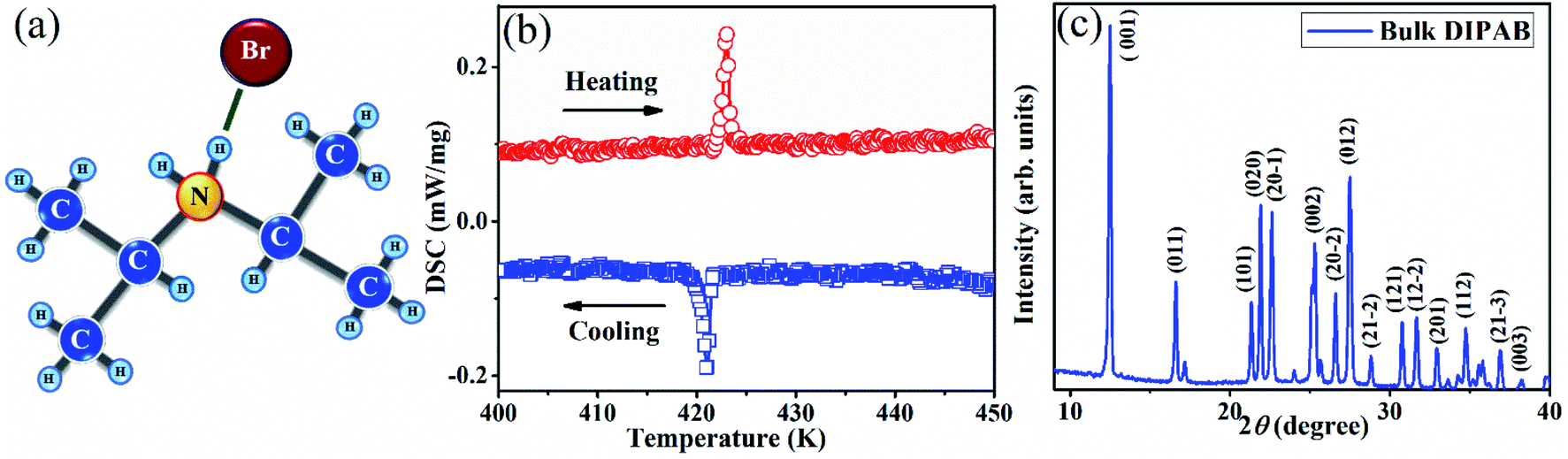 | ||
| Fig. 1 (a) Schematic diagram of DIPAB single molecular (C6H16NBr) structure. (b) DSC data recorded on the bulk sample in heating and cooling cycles and (c) XRD pattern of bulk DIPAB. | ||
The hysteretic nature of the phase transition with 4 K difference in anomalies between heating and cooling cycles confirms that the phase transition in DIPAB bulk sample is first-order in nature. As reported, the phase transition could be from the monoclinic-I (P21) phase to monoclinic-II (P21/m). Note that the irreversible orthorhombic (P212121) to monoclinic-I (P21) transition is not seen in the sample because the synthesized sample is pre-heated to 430 K before the DSC measurement which is above the TC (reversible transition). To reconfirm the structural phase of the bulk DIPAB sample, the XRD measurement is performed, and the resultant plot is shown in Fig. 1(c). The pattern is indexed to the ferroelectric monoclinic-I phase with space group P21 in comparison with literature, which is in agreement with the DSC observation.18
3.2 Structural, morphology and optical properties of DIPAB film
The DIPAB film is fabricated by thermally evaporating the bulk pellet sample and depositing it on a Si(100) substrate for 2 h. Note that slow evaporation is maintained throughout the deposition by controlling the heating power. The photograph of the grown film shown in Fig. 2(a) displays a uniform colour indicating that the film is deposited with uniform thickness. To estimate the film thickness, a cross-sectional scanning electron microscopy (SEM) image is obtained, and the same is presented in Fig. 2(b). The figure indicates that the film maintains a clear boundary with the substrate and the thickness of the film is ∼28.4 μm. The phase formation of the DIPAB film is confirmed by recording the XRD patterns. The observed XRD pattern is shown in Fig. 2(c). The pattern displays only (001), (002) and (003) diffraction peaks, which is an indication for preferred orientation of the film along c-axis. To obtain the optical bandgap, UV-Vis diffuse reflectance spectrum is recorded on the film. The obtained reflectance R is then converted into the Kubelka–Munk (K–M) function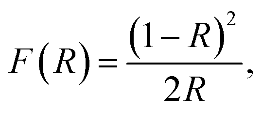 and [F(R)hν]2 is plotted as a function of hν in the inset of Fig. 2(c), where h is the Planck constant, and ν is the frequency.25 The optical bandgap is extracted from the linear fitting using a straight line equation, shown as a solid line in the inset. The intercept of the extrapolated straight line at the energy axis revealed the bandgap be ∼3.52 eV and it is a direct bandgap.
 | ||
| Fig. 2 (a) The photographic image of DIPAB/Si film. (b) Cross-sectional SEM image and (c) XRD pattern recorded on DIPAB film samples. The inset shows the K–M plot. | ||
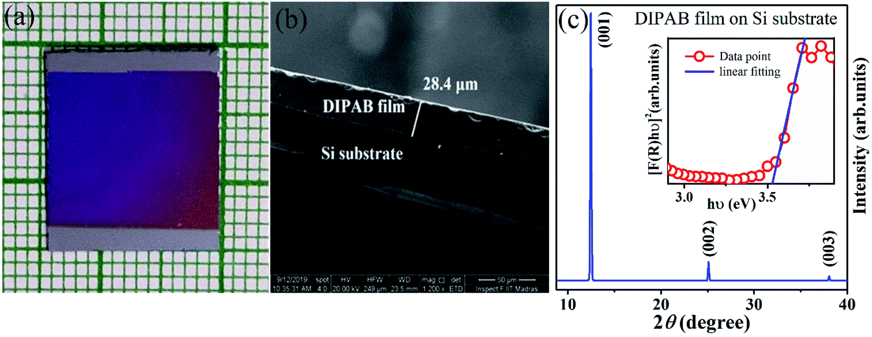
The surface morphology of the grown film is analyzed by recording FESEM and PFM topographic images. The FESEM images obtained at two different magnifications are shown in Fig. 3(a) and (b). The images reveal a well-connected grain-like growth of DIPAB film. This feature is seen throughout the surface of the film. It is noteworthy to mention that the microcrystal-like structures reported on the DIPAB films are absent in our film. To get an information about the average grain size, the respective histogram is shown in Fig. 3(c). The histogram illustrates that the grain sizes vary from 0.2 to 1.4 μm, with an average grain size of ∼0.6 μm. To elucidate it further, the PFM topographic image obtained over 5 × 5 μm2 area is shown in Fig. 3(d). The PFM image also displays similar grain-like features throughout the surface with an average roughness of ∼2 nm. The roughness profile across the scanned area is shown as an inset in Fig. 3(d). Overall, both the FESEM and PFM topographic images demonstrate that the DIPAB film on Si(100) substrate is grown with a smooth surface containing uniformly distributed well-connected grain-like morphology. The uniform growth of DIPAB is due to the manifestation of the molecules reaching the substrate with sufficient energy gained from the thermal evaporation process and thereby facilitating the necessary grain growth by the diffusion process.
 | ||
| Fig. 3 SEM surface morphology images (a and b) of DIPAB/Si(100) film. (c) Histogram showing the grain size distribution and (d) PFM topographic image of DIPAB/Si(100) film surface. The inset is the roughness profile drawn across the PFM image shown by the red-line. | ||
3.3 Ferroelectric characteristics of the film
The ferroelectric characteristics of the film are analyzed using the PFM technique both in out-of-plane and in-plane modes. Initially, the film surface is scanned by the PFM probe over 20 × 20 μm2 area with 10 V ac signal under out-of-plane mode. The observed amplitude and phase images are displayed in Fig. 4(a) and (b), respectively. The absence of clear contrast in both amplitude and phase images show that there is no preferred orientation of the domains along the out-of-plane direction. On the other hand, the amplitude and phase images recorded under in-plane mode depicted in Fig. 4(c) and (d) display a clear contrast among the domains with specific domain patterns. The images illustrate that the domains show preferred orientation along one of the in-plane direction of the film, which could be either along a- or b-axis (note that the XRD pattern confirms that the out-of-plane direction is along the c-axis). This is in agreement with the reported in-plane uniaxial polarization direction (b-axis) found in microcrystals deposited on substrate.26 Note that the DIPAB growth by solution method mostly result in needle like crystals with preferred orientation being along b-axis which is the polarization axis of the crystal. This could be due to the resultant electric field originates from the polarization favoring the faster growth rate along the b-axis. In the present case, during the thermal evaporation process, faster growth rate is preferred along the in-plane direction where the available DIPAB molecules for the growth are higher compared to the growth rate along the out-plane direction. This explains that the polarization direction (b-axis) of the grown film to be along the in-plane direction and hence the c-axis orientation of the film. The switchable ferroelectric characteristics of the film can be inferred from the amplitude and phase response of the local domains for the external bias-voltage through the PFM probe. The corresponding amplitude and phase data recorded on the sample as a function of the bias-voltage are plotted in Fig. 4(e) and (f), respectively. The amplitude plot exhibits a clear butterfly loop with two minima at −3.7 and 4.0 V bias-voltage. The observed butterfly nature of the loops elucidates the ferroelectric characteristics of the film. Additionally, the phase plot shown in Fig. 4(f) exhibits hysteretic behaviour with a 180° phase difference between the positive and negative bias-voltage. These features confirm the switchable polarization characteristics of the ferroelectric DIPAB film on Si(100) substrate. Though direct P–E measurements would be better to reiterate the switchable polarization characteristics of the DIPAB film, such a measurements are difficult in the context of polarization axis being along the in-plane direction. Attempt to measure the in-plane P–E measurements lead to the sample melting due to high voltage requirement.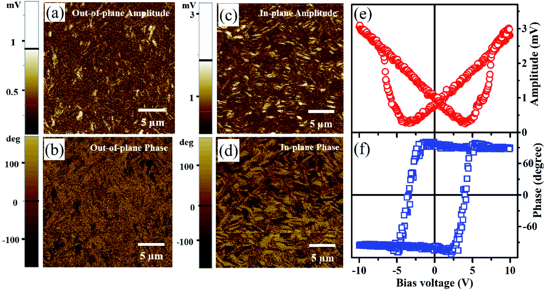 | ||
| Fig. 4 The PFM (a) out-of-plane amplitude, (b) out-of-plane phase, (c) in-plane amplitude, and (d) in-plane phase images of DIPAB/Si film. (e) The amplitude and (f) phase data plotted as a function of bias voltage for the DIPAB/Si film. | ||
3.4 Self-powered photo-detector charecteristics
In recent times, the ferroelectrics are being investigated for the photovoltaic and photodetector characteristics in both bulk and films.25,27–31 The advantage of ferroelectric system in these devices are the presence of large internal electric field called the depolarization field which could facilitates the separation of photogenerated electron–hole pairs throughout the system under zero-bias condition. Accordingly, above-bandgap photovoltage and self-biased photodetector performance are demonstrated on few ferroelectric systems. However, the photodetector characteristics of organic ferroelectric films are not yet reported in the literature. The ferroelectric DIPAB film with a bandgap of 3.52 eV could be one of the suitable candidates for UV photodetector applications. To investigate its photodetector characteristics, the measurements are carried out on the DIPAB/Si film along the in-plane direction. Note that the domains in DIPAB film are aligned along the in-plane direction as confirmed from the PFM measurements. Hence, in-plane measurement is preferable over the out-of-plane PV measurement. Accordingly, the Au electrodes are deposited in strips, with a separation distance between the electrode as 100 μm, by the thermal evaporation method. The dimension of each Au strip is 6 mm × 100 μm. The schematics of the sample geometry and the experimental set-up used to perform the PV measurement are shown in Fig. 5(a). Note that prior to the measurement, the sample is poled along the in-plane direction under 50 V for 10 minutes. The current (I) versus the applied dc voltage (V) recorded under dark reveals a non-linear curve passing through the origin as shown in Fig. 5(b). The measurements are repeated under UV-Vis light at the intensities of 11.5, 18.5, 25.6, 31.7, 38.8, and 45.8 mW cm−2. The respective I–V curves shown in Fig. 5(b) display that the DIPAB exhibits remarkable photocurrent response under UV-Vis light illumination. The DIPAB film displays a large current with a maximum value of 217 nA at 45.8 mW cm−2 light intensity. The stability of the observed photocurrent response is probed by measuring the current as a function of time in the zero-bias condition under repeated light ON and OFF states at various light intensities. Fig. 5(c), where the current at zero-bias is plotted at different light intensity, illustrates that the grown DIPAB/Si(100) film displays stable photocurrent response under self-bias condition. The response time which is the time taken for the current to reach 90% of its maximum value from its 10% is 0.27 s. The obtained value is comparable to the reported values for other ferroelectric system.32,33 The photo-current, Iph, is calculated from the plot Fig. 5(c) using the formula Iph = |ISC| − |Id|, where Id is the dark current measured under light OFF condition.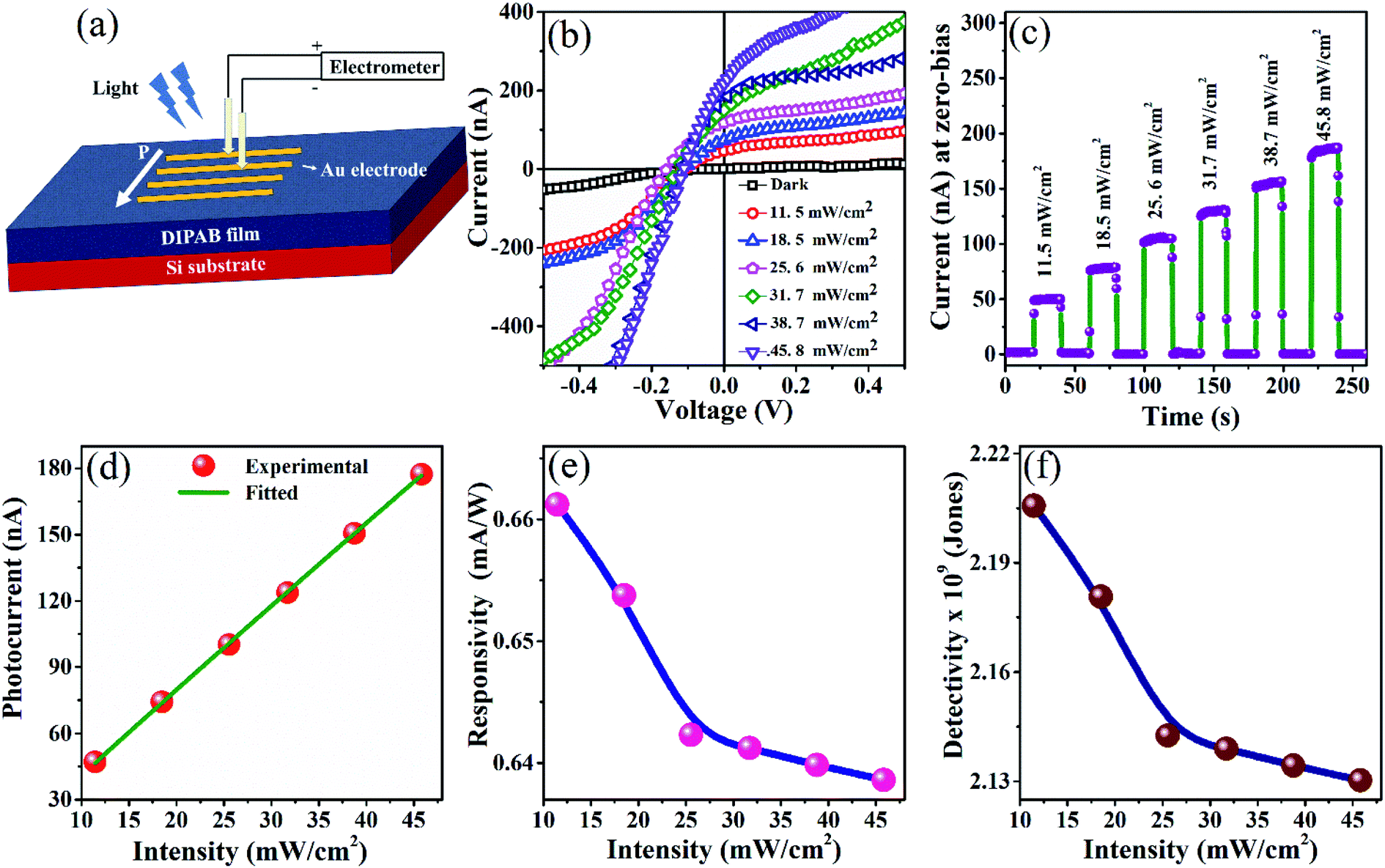 | ||
| Fig. 5 (a) Schematic of sample geometry used for the PV measurements. The P indicates the polarization direction. (b) Current versus bias voltage measured on the DIPAB/Si film under UV-Vis light with various intensities. (c) The current at zero-bias measured under repeated light ON and OFF conditions at various light intensities. (d) Photocurrent, (e) responsivity, and (f) detectivity plotted as a function of light intensity. | ||
The resultant Iph displayed against the light intensities in Fig. 5(d) shows linear behavior with light intensity. To access the photodetector capability of the DIPAB film, the experimental data shown in Fig. 5(d) is fitted with power-law Iph = αPθ, where α is a constant, P is light intensity, and θ is an empirical constant which can take the ideal value of 1. The fitting reveals that θ ∼ 0.97 and it shows better photocurrent capabilities of DIPAB film compared to other ferroelectric photodetectors.32,34 However, the deviation from the ideal value could be attributed to the recombination states and carrier–carrier interactions of the photogenerated carriers. To elucidate it further, the photodetector characteristic parameters such as the responsivity (R) and detectivity (D) are calculated from R = Iph/PS and D = R/(2eId/S)0.5, where S is light illuminated area of the sample and e is the charge.35,36 The extracted R and D values are plotted against the light intensity in Fig. 5(e) and (f), respectively. Both R and D values show a decreasing trend with the increase in light intensity. This could be due to the increase in the recombination rate at higher light intensities. The maximum value of R and D obtained are 0.66 mA W−1 and 2.20 × 10⁹ Jones at 11.45 mW cm−2. These values are comparable to the photodetector characteristics parameters reported on various organic and inorganic under self-bias condition.31,37–39 Although, the external quantum efficiency can be obtained as reported in the literature, the limitation in the experimental set-up restrict such measurement in the present work.40–42
4. Conclusion
The c-axis oriented organic ferroelectric diisopropylammonium bromide film deposition on Si(100) substrate was demonstrated by the thermal evaporation method. The surface morphological studies revealed a smooth, uniform, and well-connected grain-like features with ∼2 nm surface roughness. The PFM analysis confirms the in-plane domain orientation, which is in accordance with the c-axis orientation of the film. The phase and amplitude response of the local domains for an applied dc-bias endorsed the ferroelectric switching characteristics of the grown film. The electrical current measurements under UV-Vis light illumination on the organic ferroelectric film displayed a remarkable photocurrent response. The photodetector performance parameter extracted from the photocurrent measurements under various light intensities illustrated the application potential of the grown film in self-powered UV-Vis photodetector and other optoelectronic devices. In addition, the demonstrated continuous film fabrication can envisage the technological implication of the organic ferroelectric diisopropylammonium bromide material.Conflicts of interest
There are no conflicts to declare.Acknowledgements
P. M. acknowledge CSIR for sponsoring the project under the grant no. 03(1405)/17/EMR-II. Authors thank to Dr C. Sudakar and Dr Subhajit Nandy for diffuse reflectance measurements on DIPAB film.References
- S. L. Miller, R. D. Nasby, J. R. Schwank, M. S. Rodgers and P. V. Dressendorfer, J. Appl. Phys., 1990, 68, 12 Search PubMed
.
- P. P. Biswas, C. Thirmal, D. Duraisamy, G. N. Venkatesan, S. Venkatachalam and P. Murugavel, J. Appl. Phys., 2017, 110, 192906 Search PubMed
- B. Nagaraj, S. Aggarwal, T. K. Song, T. Sawhney and R. Ramesh, Phys. Rev. B: Condens. Matter Mater. Phys., 1999, 59, 16022 CrossRef CAS
- K. Uchino, Ferroelectric Devices, CRC Press Taylor & Francis Group, 2009 Search PubMed
- K. J. Choi, M. Biegalski, Y. L. Li, A. Sharan, J. Schubert, R. Uecker, P. Reiche, Y. B. Chen, X. Q. Pan, V. Gopalan, L. Q. Chen, D. G. Schlom and C. B. Eom, Science, 2004, 306, 1005 CrossRef CAS PubMed
- Z. Cheng, X. Wang and S. Dou, Phys. Rev. B: Condens. Matter Mater. Phys., 2008, 77, 092101 CrossRef
- Y. Xu, Ferroelectric Materials and Their Applications., North-Holland, 1991 Search PubMed
- P. K. Panda and B. Sahoo, Ferroelectrics, 2015, 474, 128 CrossRef CAS
- S. Horiuchi and Y. Tokura, Nat. Mater., 2008, 7, 357 CrossRef CAS PubMed
- D. W. Fu, W. Zhang, H. L. Cai, J. Z. Ge, Y. Zhang and R. G. Xiong, Adv. Mater., 2011, 23, 5658 CrossRef CAS PubMed
- D. W. Fu, H. L. Cai, Y. Liu, Q. Ye, W. Zhang, Y. Zhang, X. Y. Chen, G. Giovannetti, M. Capone, J. Li and R. G. Xiong, Science, 2013, 339, 435 CrossRef PubMed
- C. Jiang, W. Y. Tong, H. Lin, C. Luo, H. Peng and C. G. Duan, Phys. Status Solidi A, 2017, 214, 1700029 CrossRef
- K. Gao, M. Gu, X. Qiu, X. N. Ying, H. Y. Ye, Y. Zhang, J. Sun, X. Meng, F. M. Zhang, D. Wu, H. L. Cai and X. S. Wu, J. Mater. Chem. C, 2014, 2, 9957 RSC
- Y. Zhang, Y. Liu, H. Y. Ye, D. W. Fu, W. Gao, H. Ma, Z. Liu, Y. Liu, W. Zhang, J. Li, G. L. Yuan and R. G. Xiong, Angew. Chem., Int. Ed., 2014, 53, 5064 CAS
- H. Y. Ye, Y. Y. Tang, P. F. Li, W. Q. Liao, J. X. Gao, X. N. Hua, H. Cai, P. P. Shi, Y. M. You and R. G. Xiong, Science, 2018, 361, 151 CrossRef CAS PubMed
- S. Horiuchi, Y. Tokunaga, G. Giovannetti, S. Picozzi, H. Itoh, R. Shimano, R. Kumai and Y. Tokura, Nature, 2010, 463, 789 CrossRef CAS PubMed
- L. Ma, Y. Jia, S. Ducharme, J. Wang and X. C. Zeng, J. Am. Chem. Soc., 2019, 141, 1452 CrossRef CAS PubMed
- A. Piecha, A. Gagor, R. Jakubas and P. Szklarz, CrystEngComm, 2013, 15, 940 RSC
- K. Ga, C. Xu, Z. Cui, C. Liu, L. Gao, C. Li, D. Wu, H. L. Cai and X. S. Wu, Phys. Chem. Chem. Phys., 2016, 18, 7626 RSC
- S. Poar, H. Lu, J. Song, O. Goit, S. Valloppilly, A. Gruverman and S. Duchme, J. Phys. D: Appl. Phys., 2016, 49, 505305 CrossRef
- C. Thirmal, P. P. Biswas, Y. J. Shin, T. W. Noh, N. V. Giridharan, A. Venimadav and P. Murugavel, J. Appl. Phys., 2016, 120, 124107 CrossRef
- I. Bernti, G. Ruani, F. Liscio, S. Milita, F. Dinelli, X. Xu, E. Wang and M. Cvallini, Langmuir, 2017, 33, 12859 CrossRef PubMed
- S. Biswas, O. Shalev and M. Shtein, Annu. Rev. Chem. Biomol. Eng., 2013, 4, 289 CrossRef CAS PubMed
- J. L. Vossen and W. Kern, Thin film process, Academic Press Limited, 1991 Search PubMed
- S. Pal, A. B. Swain, P. P. Biswas, D. Murali, A. Pal, B. R. K. Nanda and P. Murugavel, Sci. Rep., 2018, 8, 8005 CrossRef PubMed
- H. Lu, T. Li, S. Poddar, O. Goit, A. Lipatov, A. Sinitskii, S. Ducharme and A. Gruverman, Adv. Mater., 2015, 27, 7832 CrossRef CAS PubMed
- P. P. Biswas, C. Thirmal, S. Pal and P. Murugavel, J. Appl. Phys., 2018, 123, 024101 CrossRef
- L. You, F. Zheng, L. Fang, Y. Zhou, L. Z. Tan, Z. Zhang, G. Ma, D. Schmidt, A. Rusydi, L. Wang, L. Chang, A. M. Rappe and J. wang, Sci. Adv., 2018, 4, 7 Search PubMed
- J. Wang, J. Ma, Y. Yang, M. Chen, J. Zhang, J. Ma and C. W. Nan, ACS Appl. Electron. Mater., 2019, 1, 862 CrossRef CAS
- P. P. Biswas, S. Pal, V. Subramanian and P. Murugavel, Appl. Phys. Lett., 2019, 114, 173901 CrossRef
- X. Liu, S. Wang, P. Long, L. Li, Y. Peng, Z. Xu, S. Han, Z. Sun, M. Hong and J. Luo, Angew. Chem., Int. Ed., 2019, 58, 14504 CrossRef CAS PubMed
- P. P. Biswas, S. Pal, V. Subramanian and P. Murugavel, J. Phys. D: Appl. Phys., 2020, 53, 27 CrossRef
- N. Ma and Y. Yang, Nano Energy, 2019, 40, 352 CrossRef
- D. Zheng, J. Wang, W. Hu, L. Liao, H. Fang, N. Guo, P. Wang, F. Gong, X. Wang, Z. Fan, X. Wu, X. Meng, X. Chen and W. Lu, Nano Lett., 2016, 16, 2548 CrossRef CAS PubMed
- W. Feng, X. Wang, J. Zhang, L. Wang, W. Zheng, P. Hu, W. Cao and B. Yang, J. Mater. Chem. C, 2014, 2, 3254 RSC
- J. Wang, J. Han, X. Chen and X. Wang, InfoMat, 2019, 1, 33 CrossRef
- J. Miao and F. Zhang, J. Mater. Chem. C, 2019, 7, 1741 RSC
- A. B. Swain, M. Rath, P. P. Biswas, M. S. R. Rao and P. Murugavel, APL Mater., 2019, 7, 011106 CrossRef
- S. Wang, L. Li, W. Weng, C. Ji, X. Liu, Z. Sun, W. Lin, M. Hong and J. Luo, J. Am. Chem. Soc., 2020, 142, 55 CrossRef CAS PubMed
- Z. Zhao, C. Li, L. Shen, X. Zhangc and F. Zhang, Nanoscale, 2020, 12, 1091 RSC
- W. Wang, F. Zhang, M. Du, L. Li, M. Zhang, K. Wang, Y. Wang, B. Hu, Y. Fang and J. Huang, Nano Lett., 2017, 17, 1995 CrossRef CAS PubMed
- Z. Zhao, J. Wang, C. Xu, K. Yang, F. Zhao, K. Wang, X. L. Zhang and F. Zhang, J. Phys. Chem. Lett., 2020, 2, 366 CrossRef PubMed
| This journal is © The Royal Society of Chemistry 2020 |