
 Open Access Article
 This Open Access Article is licensed under a Creative Commons Attribution-Non Commercial 3.0 Unported Licence
Simulation-guided nanofabrication of high-quality practical tungsten probes
Chengye Dong†
 a,
Guodong Meng†*a,
Sandra Elizabeth Sajib,
Xinyu Gaoa,
Pengcheng Zhangc,
Di Wud,
Yi Pand,
Zongyou Yin*b and
Yonghong Cheng*a
a,
Guodong Meng†*a,
Sandra Elizabeth Sajib,
Xinyu Gaoa,
Pengcheng Zhangc,
Di Wud,
Yi Pand,
Zongyou Yin*b and
Yonghong Cheng*a
aState Key Laboratory of Electrical Insulation and Power Equipment, Xi'an Jiaotong University, Xi'an, 710049, China. E-mail: gdmengxjtu@xjtu.edu.cn; cyh@xjtu.edu.cn
bResearch School of Chemistry, The Australian National University, Canberra, Australian Capital Territory 2601, Australia. E-mail: zongyou.yin@anu.edu.au
cCenter for Advancing Materials Performance from the Nanoscale (CAMP-Nano), State Key Laboratory for Mechanical Behavior of Materials, Xi'an Jiaotong University, Xi'an 710049, China
dCenter for Spintronics and Quantum Systems, State Key Laboratory for Mechanical Behavior of Materials, Xi'an Jiaotong University, Xi'an 710049, China
First published on 25th June 2020
Abstract
Micro/nanoscale tungsten probes are widely utilized in the fields of surface analysis, biological engineering, etc. amongst several others. This work performs comprehensive dynamic simulations on the influences of electric field distribution, surface tension and the bubbling situation on electrochemical etching behaviors, and then the tip dimension. Results show that the etching rate is reliant on the electric field distribution determined by the cathode dimension. The necking position lies in the meniscus rather than at the bottom of the meniscus. A bubble-free condition is mandatory to stabilize the distribution of OH− and WO42− ions for a smooth tungsten probe surface. Such simulation-guidance enables the nanofabrication of probes with a high aspect ratio (10![[thin space (1/6-em)]](https://www.rsc.org/images/entities/char_2009.gif) :1), ultra-sharp tip apex (40 nm) and ultra-smooth surface. These probes have been successfully developed for high-performance application with Scanning Tunneling Microscopy (STM). The acquired decent atomic resolution images of epitaxial bilayer graphene robustly verify the feasibility of the practical level application of these nanoscale probes. Therefore, these nanoscale probes would be of great benefit to the development of advanced analytical science and nano-to-atomic scale experimental science and technology.
:1), ultra-sharp tip apex (40 nm) and ultra-smooth surface. These probes have been successfully developed for high-performance application with Scanning Tunneling Microscopy (STM). The acquired decent atomic resolution images of epitaxial bilayer graphene robustly verify the feasibility of the practical level application of these nanoscale probes. Therefore, these nanoscale probes would be of great benefit to the development of advanced analytical science and nano-to-atomic scale experimental science and technology.
1 Introduction
Due to excellent thermal and electrical conductivity, high mechanical strength and a simple fabrication process, micro/nanoscale tungsten probes have been universally employed in various fields such as microanalysis of materials (scanning probe methods),1–5 biological technology,6,7 manipulator systems8 and others.9–13 Compared to mechanical methods,14–17 flame etching18 and others,19,20 electrochemical etching of tungsten wire has been extensively adopted due to its convenience, reliability and easy operation.21–24 A number of etching strategies and methods, including the drop-off method,23 liquid membrane etching,25 two-step etching,26 inversing etching27 and post-annealing,28 have been developed for the fabrication of various probes. Among them, the drop-off method is the most popular one due to its convenient operability and high controllability. With the drop-off method, the influence of different etching parameters on the profile and roughness of the probes have been explored, including strategies for the applied voltage between electrodes, mass of immersed part, relative location of electrodes, motion modes of the anode and electrolyte concentration.29–32 Meanwhile, various probes have been fabricated to meet different demands. For example, Li et al. fabricated different probes with controllable aspect ratio based on the investigation on the relation between pulling up speed, time and aspect ratio.33 Ju et al. reported the fabrication of micro/nanoscale tungsten probes with controllable tip profiles of exponential, conical, multi-diameter, and calabash-like shapes.29Although numerous works have explored the etching process to get specific tungsten probes, the majority of these works focused on reducing the tip radius and only a handful of them discussed the etching mechanisms behind the experimental parameters. For instance, Ibe et al. discussed the chemical reaction mechanism and the initial voltage to activate the etching.34 Xu et al. investigated the influence of the voltage and the meniscus on the roughness and radius of the probe.35 Kulakov et al. reported the motion law of the ions during the etching process according to experimental estimate of the film density and interfacial tension.21 Since most of the reported works are experimental studies, it is hard to get an in-depth understanding of the actual roles of the electric field between the electrodes, interfacial interaction and ionic diffusion caused by the bubbling effect during the etching process. Hence, it is of great significance to comprehensively understand the roles that the electric field, interfacial interaction and ionic diffusion play in the fabrication of tungsten probes by systematically combining both experiments and numerical computation.
Herein, this paper presents the experimental and simulation investigations on the influences of the electric field distribution, interfacial interaction and ionic diffusion on the contour and shape of the tungsten probes. The Comsol Multiphysics software is employed to simulate the dynamic etching process and the results have been proved to agree well with the experimental results. Furthermore, the mechanism of fabricating different probes is discussed. The fabrication system is optimized and various probes with different apex radii, high aspect ratio, ultra-sharp tip apex, ultra-smooth surface and multi-diameter are fabricated. The success of fabricating these probes not only verifies the proposed influence mechanism but also provides opportunities to utilize tungsten in multi-probe systems,36 biological systems,37 electric field emission systems38,39 and so on.
2 Experimental
2.1. Formation of tips
With the voltage applied between the electrodes, the electrochemical etching of the tungsten wire begins and proceeds via the following reactions:Anode reaction:
| W(s) + 8OH−(aq) = WO42−(aq) + 4H2O(l) + 6e− | (1) |
Cathode reaction:
| 6H2O(l) + 6e− = 3H2(g) + 6OH−(aq) | (2) |
Overall reaction:
| W(s) + 2OH−(aq) + 2H2O(l) = WO42−(aq) + 3H2(g) | (3) |
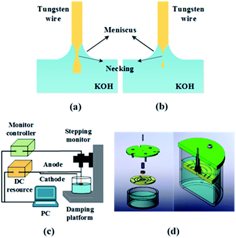 | ||
| Fig. 1 Etching process: meniscus is formed at the interface between tungsten wire and solution. With the voltage applied, (a) necking (b) dropping off of the tungsten wire will take place and micro/nanoscale tip will be obtained; (c) the schematic diagram of electrochemical etching system employed in this work; (d) customized electrode systems employed in this work, the grey is tungsten wire, the green is fastener, the blue is isolating tube with a diameter of 4 mm, the brown is copper ring cathode and the yellow is supporting device. All the components are seated in the beaker with KOH solution and copper ring cathode, supporting device and part of insulating tube and tungsten wire are immersed in the solution. Voltage is applied between the tungsten wire and the copper ring cathode. | ||
2.2. Experimental setup
The schematic of the customized etching system is shown in Fig. 1(c) and (d). A stepping motor (TSTA-1050, 7-star, Beijing), holding the 99.97% pure tungsten wire with a diameter of 0.5 mm, is used to control the motion mode of the anode. The tungsten wire is immersed into the electrolyte (2 M KOH) vertically. An isolating tube, sitting between the tungsten wire and the cathode, is developed to prevent bubbles, released from cathode, affecting the electrolyte around the tungsten wire. DC voltage is chosen to be applied to the electrodes since it is more favourable to prepare probes with both high aspect ratio and nanoscale tips.30 A DC power source (B2091A, Keysight, USA) supplies different power modes to the tungsten anode and the ring copper cathode. Both the monitor and the power source could be programmed by the computer so that we can accurately control the motion of anode and immediately cut off the power once the immersed part of tungsten wire detaches from the upper part. Polymethyl methacrylate (PMMA) is utilized as an alkali-resistant coating on the tungsten wire.2.3. Numerical simulation
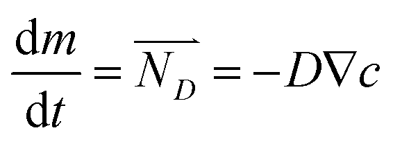
All the simulations are conducted in the Comosol Multiphysics software based on the finite element method which subdivides a large system into finite smaller and simpler parts by meshing the model. The etching process is analyzed by solving partial differential equations with defined boundary values. Based on the etching principle, three main parts, which are the distribution of the electric field in the electrolyte, concentration variation of WO42− and OH− ions and ionic motion, are considered in the simulations during the etching process. The simulations are conducted based on the following assumptions and equations:1. The voltage applied to the electrodes is constant. During the etching process, the distribution of the electric field in the electrolyte changes along with the etching of the tungsten wire. The distribution of current density in the electrolyte is calculated by the following equations:
 | (4) |
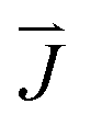 is the current density in the electrolyte,
  is the initial current density, which is taken as 0 in the simulations, σ is the conductivity of the electrolyte, σKOH ≈ 0.35 S cm−1,40
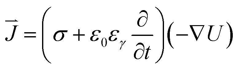
  is the electrical strength in the electrolyte, which is taken equal to −∇U, U is the voltage applied to the electrodes,
  is the electric displacement vector, which is taken equal to
  , ε0 is the dielectric constant of vacuum, εγ is the relative permittivity of the electrolyte, εrKOH ≈ 55,41 t is the time.
Then the distribution of current density in the electrolyte can be calculated with the initial voltage applied to the electrodes by eqn (5).
 | (5) |
2. The motion of WO42− and OH− ions are driven by ionic concentration difference and electric field simultaneously without the influence of H2 bubbles. The diffusion caused by concentration difference is simulated by the Fick's first law shown in eqn (6).
 | (6) |
 is the diffusion flux, D is the coefficient of diffusion, DK+ = 1.960 × 10⁻⁹ m2 s−1, DOH−1 = 5.270 × 10⁻⁹ m2 s−1,
  is defined as 5 × 10⁻¹⁰ m2 s−1,42 c is the concentration of the ions.
The migration of WO42− and OH− ions driven by electric field is calculated by the eqn (7).
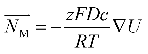 | (7) |
 is the migration flux, z is the electric charge quantity of the ions, F is the Faraday constant, D is the diffusion coefficient of ions, c is the concentration of the ions, R is the gas constant, R = 8.314 J mol−1 K−1, T is the temperature, T = 298.15 K, U is the voltage applied to the electrodes.
3. At the boundary between the tungsten wire and the electrolyte, the consumption rate of the OH− ions is proportional to the current density and is defined twice as high as the generating rate of WO42− ions based on the overall electrochemical reaction.
4. As the etching system is axisymmetric, a 2-dimensional model is built to simplify the simulations. Non-conformal meshing is employed in the simulations. The size of grids in the meniscus and at the interface between electrodes and electrolyte are less than 10 μm. In order to speed up the simulation, the size of all the other grids are no more than 1 mm.
5. The etching parameters used in the simulation are shown in Table 1.
| Parameters | Values | |
|---|---|---|
| Length of the immersed tungsten probe | 3 mm | |
| Diameter of the tungsten probe | 0.5 mm | |
| Diameter of the cathode ring | 10 mm | |
| Length of the resistant coating | 0.2 mm | |
| Concentration of KOH | 2 M | |
| Voltage applied between the electrodes | 15 V | |
3 Results and discussion
3.1. Influence of electric field
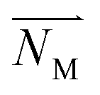
When voltage is applied to the electrodes, the electric field in the electrolyte will drive the ions toward the electrodes. During the etching process, the tungsten wire immersed in the electrolyte is etched gradually and the boundary between the tungsten wire and the electrolyte changes. That is to say, the electric field distribution in the electrolyte will change along with the etching process. The change of the electric field will lead to migration of ions and have a significant influence on the etching process. In order to simplify the simulation, the current density is employed to represent the change of the ionic distribution as the current in the electrolyte is formed by the motion of ions in the electric field.The etching appliance (the ring cathode with a diameter of 10 mm) in Fig. 2(a) is designed to study the effect of the electric field. The isolating tube, made of polytetrafluoroethylene, will not change the electric field distribution between the electrodes, thereby providing help to get rid of the bubble effect. Moreover, an alkali-resistant coating on the tungsten wire is employed to protect the part in the meniscus from etching. As is demonstrated in Fig. 2(b) (t = 0 s) and Fig. 2(c) (t = 11.9 s), the distribution of current density in the electrolyte with different etching times indicates that the maximum current density is at the end of the immersed part (point A in Fig. 2(a)). Furthermore, Fig. 2(d) shows that the current density along the tungsten wire with a 10 mm ring cathode decreases from 4.7 × 10⁴ A m−2 (point A) to 2.7 × 10⁴ A m−2 (point B) at t = 11.9 s. Since the alkali-resistant coating is regarded as a piece of slice, the grids around point B are distorted in the simulation process leading to a sharp increase in the current density when approaching to point B. According to both simulation and experimental results shown in Fig. 2(c) and (e), the tip will be formed at the end of the wire and the contour of the immersed part is conical, which proves that the etching rate of tungsten wire has a positive correlation with the current density nearby, provided there are no bubbles and meniscus in the etching region.
 | ||
| Fig. 2 The effect of electric field. (a) The schematic of etching appliance, including an isolating device to prevent bubbles released from the cathode from disturbing the solution around the tungsten wire, tungsten wire with an alkali-resistant coating to prevent tungsten in the meniscus from being etched and a ring cathode with a diameter of 5 or 10 mm. Position A is the end of the tungsten probe and position B is the bottom of the alkali-resistance coating. (b) When t = 0 s, current density around the tungsten wire in the electrolyte is obtained by the simulation. The scale bar in the inert image is 300 μm and the color scale is for amplitude of the current density in the electrolyte. (c) When t = 11.9 s, current density around the etched tungsten probe. The color scale is for amplitude of the current density in the electrolyte; (d) current density along the tungsten probe with diameters of 5 and 10 mm; (e) SEM image of tungsten probe prepared with the etching appliance shown in (a), and the diameter of the ring electrode is 10 mm. | ||
As shown in Fig. 2(d), the ring cathode with a smaller diameter of 5 mm could drive the higher current density region as well as the position of the maximum current density towards the surface of the electrolyte due to the redistribution of the electric field. The location of necking is now at point B in Fig. 2(a). And the etching rate increases at the necking position since the maximum current density of smaller ring cathode is higher, which means that decreasing the diameter of the ring cathode will reduce the preparation time and improve the production efficiency of tungsten probes. However, the smaller diameter cathode could also lead to a greater gradient of the current density between the necking position and the end of the tungsten wire, which will relatively reduce the etched amount of the immersed part before it drops off. Therefore, a much heavier end will drop off and depart from the probe while the necking region still has a relatively large diameter, which is not beneficial for preparing ultra-sharp tips. Additionally, H2 bubbles, being closer to the meniscus with a smaller cathode, will be another factor that influences the quality of the probe.
During the etching process, the electric field will drive the ions and affect their distribution along the tungsten wire. When different cathode rings with different diameters are employed, the electric field distribution will change and dramatically affect the necking position, the etching time and the radius of the tip. Hence, different cathode rings should be chosen to balance the radius of the tips and the time consumption while fabricating different probes.
3.2. Influence of surface tension
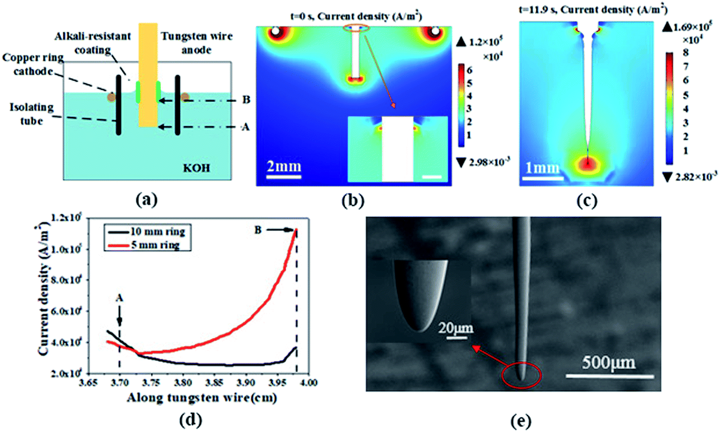
Based on the results with the alkali-resistant coating shown in Fig. 2(e), there will be no formation of necking when the part of the tungsten wire in the meniscus is protected from etching. But dropping off of the immersed tungsten wire will occur when the probe is without the alkali-resistant coating, shown in Fig. 3(d). It clearly indicates that the meniscus caused by surface tension is the key to the formation of necking which is vital to fabricate ultra-sharp tips. The necking process could be explained by the diffusion and migration of ions due to concentration difference and electric field.21 The simulation shown in Fig. 3(e) certifies the result and provides an evidence that the necking occurs at the position inside the meniscus (from position A to B shown in Fig. 3(c)) rather than at the bottom of the meniscus (at position B shown in Fig. 3(c)) which is accepted by many papers.29,31–33,35,43 Since the electric field is another factor that affects the maximum etching position on the tungsten wire, the actual necking position will vary in the meniscus with different electrodes.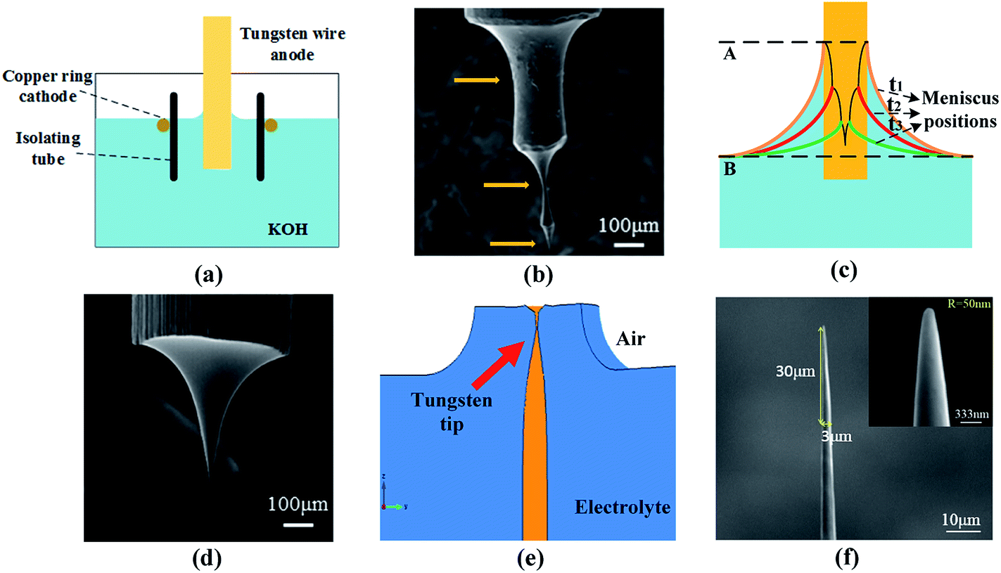 | ||
| Fig. 3 The effect of surface tension. (a) Etching appliance, including an isolating device to prevent bubbles released from the cathode from disturbing the solution around the tungsten wire and a ring cathode with a diameter of 10 mm. (b) A special probe fabricated under the situation of static etching with constant current of 0.03 A. Three necking positions are noted by the yellow arrows. (c) The schematic indicates the lifting of meniscus. The brown, red and green contour lines represent different position of the meniscus during the etching process. The black line represents the profile of the probe fabricated under the condition that meniscus had lifted twice. t1, t2 and t3 represent different moments when the meniscus moves. (d) SEM image of tungsten probe etched by the etching appliance shown in (a) with a constant voltage of 15 V. (e) The simulation result of the etching process with the same etching parameters as in (d). (f) SEM images of the fabricated probe with high aspect ratio and ultra-sharp apex. The inset shows the probe's radius of apex and conical shape (×30000). The etching parameters are set as follows, the diameter of the ring cathode: 10 mm, electrolyte concentration: 2 M, immersed depth: 3 mm, step down etching current from 0.1 A to 0.01 A and different probes will require different times to get the sharp tip at 0.01 A, reciprocation motion distance and velocity: 4 mm and 0.5 mm s−1. | ||
Fig. 3(b) shows a special probe fabricated under the condition of static etching with a constant current of 0.03 A. It is another evidence that the necking position is in the meniscus instead of at the bottom of the meniscus. There are three necking positions noted in Fig. 3(b), which will never be obtained if the necking position is at the bottom of the meniscus. Moreover, it indicates that the meniscus will move downwards during the etching process. As the etching begins, the resistance in the circuit will increase due to the gradual decrease in the diameter of the immersed part. Since the probe is fabricated with constant current, the voltage between electrodes will increase leading to increasing of the ionic concentration in the meniscus. Once the gravity of the solution in the meniscus is larger than the capillary force, the meniscus will be pulled downwards. As demonstrated in Fig. 3(c), the meniscus has been pulled downwards twice and leads to the fabrication of the probe with several diameters.
Based on the discussion above, necking occurs in the meniscus if the tungsten wire remains static during the etching process. It means that the aspect ratio of the fabricated probe will be limited. Therefore, dynamic etching should be employed to broaden the etched region of the probes if probes with various aspect ratio are required. In this work, a stepping motor, precisely controlled by a computer program, is employed to hold and control the tungsten wire to realize reciprocation motion, which is a repetitive up and down linear motion with a specific speed, instead of unidirectional motion. The aspect ratio of probes could be tuned by changing the distance and velocity of the reciprocation motion. Fig. 3(f) depicts that a probe with a high aspect ratio (10:1) and ultra-sharp apex (R = 50 nm), which is among the sharpest ones up to date as far as we know, can be fabricated with the dynamic etching method. These probes are of great importance for multipoint contact measurement and scanning probe microscopy.44–47
3.3. Influence of ionic diffusion caused by H2 bubbles
As H2 bubbles are released from the cathode during the etching process, the ionic diffusion driven by bubbles becomes another key factor influencing the fabrication of nanoscale probes. Fig. 4(a) shows the simulation models with bubbles located in different positions (P1-near cathode, P2-near tungsten wire), that are built to investigate how the bubbles affect the ionic distribution along the tungsten wire. As is exhibited in Fig. 4(d) and (e), the concentration distribution of both OH− and WO42− ions are dramatically affected when the bubbles enter the region near the meniscus (noted by the green oval). During the etching process, plenty of bubbles irregularly move to the tungsten wire which means that the concentration distribution of ions is severely perturbed. It results in the irregular fluctuation of the ionic concentration distribution along the tungsten wire. This causes severe local change of the etching rate which is responsible for the rough surface of tungsten probes. Meanwhile, the meniscus, which is vital to necking, becomes unstable when the bubbles escape from the electrolyte without the isolating tube. It brings about the unstable necking process and severely affects the surface and curvature radius of the tips. Fig. 4(b) and (c) show the probes fabricated without and with the isolating tube, respectively. Since the isolating tube can prevent bubbles moving to the immersed tungsten wire, the contour and surface condition of the probe fabricated with the isolating tube is much better. The experimental results agree well with the simulation results, which clearly indicate that the surface of the tungsten probe is seriously affected due to the destabilization of ionic concentration when the bubbles enter the meniscus without isolating devices. | ||
| Fig. 4 The effect of ionic diffusion. (a) The simulation model built to explore the effect of H2 bubbles on the etching process. The bubble with a diameter of 0.2 mm is located at different positions (P1 & P2). (b) Probe fabricated without the isolating device. (c) Probe fabricated with the isolating device. The scale bar is 5 μm. The probes are prepared under static etching with a constant voltage of 15 V and a 10 mm ring cathode. (d) t = 5 s, the concentration distribution of OH− and WO42− ions along the tungsten wire with bubbles and without bubbles near the tungsten wire in the simulation. The data around the meniscus is highlighted in the green oval. (e) SEM image of the fabricated probe with ultra-smooth surface fabricated with the isolating tube. The etching parameters are set as follows, the diameter of the ring cathode: 6 mm, electrolyte concentration: 2 M, immersed depth of tungsten wire: 4 mm, step down etching current from 0.1 A to 0.01 A and different probes will require different times to get the sharp tip at 0.01 A, reciprocation motion distance and velocity: 3 mm and 0.25 mm s−1. | ||
Since the irregular motion of bubbles during the etching process has a negative influence on the surface roughness of the probe, an isolating tube is employed to prevent the bubbles perturbing the ionic distribution. The fabricated ultra-smooth probe with a diameter of 40 nm is shown in Fig. 4(f) and there are no visible pits and protrusions on its surface. These probes with low surface roughness are vital to realize consistent and reproducible measurements. Additionally, they can be employed as nano- and micro-scale electrodes in various fields.9,12
3.4. Practical application of fabricated tungsten probes
Since the probe is the core component inside a Scanning Tunnelling Microscope (STM) for exploring ultra-fine morphology and structure of materials at atomic scale, the characteristics of the probe including its apex radius, contour, aspect ratio and surface condition, determine the resolution and sensitivity of the STM images.In order to verify the quality and functional application of tungsten probe fabricated in this work, the probe shown in Fig. 4(f) is employed as a STM probe to image epitaxial bilayer graphene on a 4H–SiC (0001) substrate. The bilayer graphene is prepared by annealing the SiC substrate at 1750 °C for 10 min in argon atmosphere. All the STM images are taken by Createc LT-STM system at 78 K in ultra-high vacuum. The tunnelling current is 0.5 nA with the sample bias of 0.1 V. Fig. 5(a) shows the atomic resolution image of the surface carbon atoms in a smooth and sharp contour using the present tungsten tip. A hexagonal lattice instead of the honeycomb lattice can been clearly verified due to the AB stacking of bilayer graphene, with an imaging resolution of approximately 0.62 Å. Fig. 5(b) shows a 6-fold symmetric structure defect on the top layer of the lattice using the present tungsten tip.
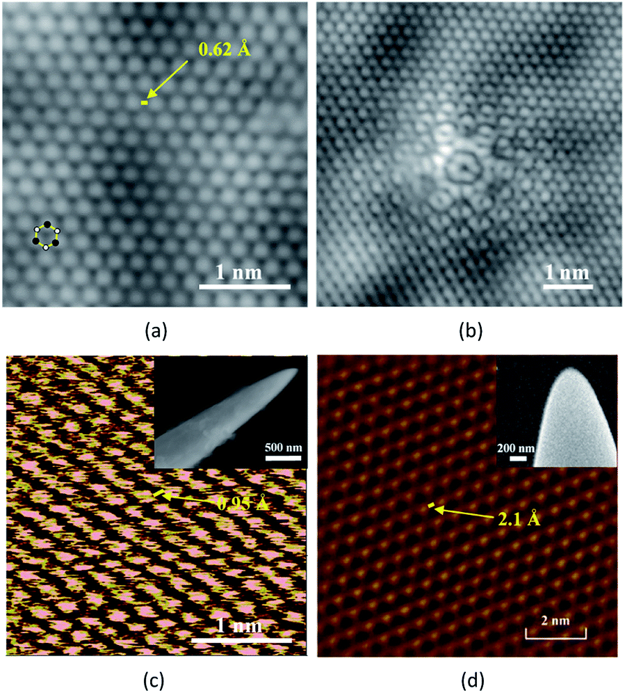 | ||
| Fig. 5 Application of fabricated tungsten probes. Topographic STM image of epitaxial bilayer graphene on a 4H–SiC (0001) substrate: (a) atomic resolution of the surface carbon atoms; (b) 6-fold symmetric structure defect on the top layer of the lattice. (c) The STM image of highly oriented pyrolytic graphite (HOPG) obtained in ref. 28 by the tungsten probe shown in the insert SEM image. The sample bias is 770 mV. The radius of the tungsten tip is 20 nm; (d) the STM image of highly oriented pyrolytic graphite (HOPG) obtained in ref. 46 by the tungsten probe shown in the insert SEM image. The tunneling current is 0.1 nA with the sample bias of 800 mV. The radius of the tungsten tip is 30 nm. Adapted with permission from ref. 27 and 45. | ||
For comparison, Fig. 5(c) and (d) show the STM images of highly oriented pyrolytic graphite (HOPG) in other works also by their electrochemically fabricated tungsten probes,27,45 demonstrating an imaging resolution of 0.95 Å and 2.1 Å, respectively. Therefore, it is clearly indicated that the STM images in this work are with higher quality and finer resolution. Hence, it can be claimed that the probe with nanoscale tip, high aspect ratio and ultra-smooth surface, which is fabricated in this work, is favourable and suitable for acquiring atomic resolution image with high quality as STM probes.
4 Conclusions
In this work, the influences of electric field, surface tension and bubbles situations on electrochemical fabrication of nanoscale tungsten probes are investigated and improved by systematically combining both experimental and dynamic simulation methods. Results show that the cathode dimension and the electric field distribution between electrodes determine the etching rate of the probe. The necking position is in the meniscus rather than at the bottom of the meniscus. Isolating the bubbles from the tungsten probe and stabilizing the concentration distribution of both OH− and WO42− ions along the tungsten probe will be vital to prepare probe with smooth surface. Based on the simulation-guided nanofabrication method, specific tungsten probes with ultra-smooth surface, nanoscale ultra-sharp apex radius (<40 nm), high aspect ratio (10:1) and multi-diameter are fabricated. High-quality atomic resolution STM images of epitaxial graphene are obtained with the fabricated probes and verify that the probes are with high quality and fit for atomic scale research as a STM probe. The mechanism for the electrochemical etching and the improved etching system are of importance to the experimental techniques in the fields of microanalysis, biological technology, nanoscale electrodes and manipulator systems.
Conflicts of interest
There are no conflicts to declare.Acknowledgements
G. M. gratefully acknowledges funding from National Natural Science Foundation of China (51977169, 51607138) and the Fundamental Research Funds for the Central University (xzy012019030). Z. Y. gratefully acknowledges the support from the ANU Futures Scheme (Q4601024) and the Australian Research Council (DP190100295, LE190100014). Y. P. gratefully acknowledges the support from the National Natural Science Foundation of China (11704303) and the National Key R&D Program of China (2017YFA0206202). The authors also acknowledge funding supported by State Key Laboratory of Electrical Insulation and Power Equipment (EIPE19203).References
- C. G. Zoski, J. Electrochem. Soc., 2016, 163, H3088–H3100 CrossRef CAS.
- S. M. Hus, X. G. Zhang, G. D. Nguyen, W. Ko, A. P. Baddorf, Y. P. Chen and A. P. Li, Phys. Rev. Lett., 2017, 119, 137202 CrossRef PubMed.
- G. Han and H. S. Ahn, Ultramicroscopy, 2016, 161, 66–73 CrossRef CAS PubMed.
- E. L. Silva, A. C. Bastos, M. A. Neto, R. F. Silva, M. L. Zheludkevich, M. G. S. Ferreira and F. J. Oliveira, Electrochim. Acta, 2012, 76, 487–494 CrossRef CAS.
- M. Hoummady and H. Fujita, Nanotechnology, 1999, 10, 29–33 CrossRef CAS.
- M. Abdolahad, A. Saeidi, M. Janmaleki, O. Mashinchian, M. Taghinejad, H. Taghinejad, S. Azimi, M. Mahmoudi and S. Mohajerzadeh, Nanoscale, 2015, 7, 1879–1887 RSC.
- G. Lu, H. De Keersmaecker, L. Su, B. Kenens, S. Rocha, E. Fron, C. Chen, P. Van Dorpe, H. Mizuno, J. Hofkens, J. A. Hutchison and H. Uji-I, Adv. Mater., 2014, 26, 5124–5128 CrossRef CAS PubMed.
- J. Comtet, A. Niguès, V. Kaiser, B. Coasne, L. Bocquet and A. Siria, Nat. Mater., 2017, 16, 634–639 CrossRef CAS PubMed.
- S. Li and R. R. Jones, Nat. Commun., 2016, 7, 13405–13411 CrossRef CAS PubMed.
- X. Ma, M. Grüßer and R. Schuster, Appl. Phys. Lett., 2015, 106, 241103 CrossRef.
- K.-T. Lin, S. Komiyama and Y. Kajihara, Opt. Lett., 2016, 41, 484–487 CrossRef CAS PubMed.
- G. Meng, Y. Cheng, K. Wu and L. Chen, IEEE Trans. Dielectr. Electr. Insul., 2014, 21, 1950–1956 CAS.
- G. Meng, X. Gao, A. M. Loveless, C. Dong, D. Zhang, K. Wang, B. Zhu, Y. Cheng and A. L. Garner, Phys. Plasmas, 2018, 25, 82116 CrossRef.
- H.-W. Fink, IBM J. Res. Dev., 1986, 30, 460–465 CAS.
- G. Binnig, H. Rohrer, C. Gerber and E. Weibel, Phys. Rev. Lett., 1982, 49, 57–61 CrossRef.
- P. J. Bryant, H. S. Kim, Y. C. Zheng and R. Yang, Rev. Sci. Instrum., 1987, 58, 1115 CrossRef.
- Y. Akama, E. Nishimura, A. ss Sakai and H. Murakami, J. Vac. Sci. Technol., A, 1990, 8, 429–433 CrossRef CAS.
- T. Yamaguchi, E. Inami, Y. Goto, Y. Sakai, S. Sasaki, T. Ohno and T. K. Yamada, Rev. Sci. Instrum., 2019, 90, 63701 CrossRef PubMed.
- J. Onoda and S. Mizuno, Appl. Surf. Sci., 2011, 257, 8427–8432 CrossRef CAS.
- A. N. Chaika, N. N. Orlova, V. N. Semenov, S. A. Krasnikov, M. G. Lazarev, S. V Chekmazov, V. G. Glebovsky, S. I. Bozhko and I. V Shvets, Sci. Rep., 2014, 4, 3742 CrossRef CAS PubMed.
- M. Kulakov, I. Luzinov and K. G. Kornev, Langmuir, 2009, 25, 4462–4468 CrossRef CAS PubMed.
- O. L. Guise, J. W. Ahner, M. C. Jung, P. C. Goughnour and J. T. Yates, Nano Lett., 2002, 2, 191–193 CrossRef CAS.
- M. Kulawik, M. Nowicki, G. Thielsch, L. Cramer, H. P. Rust, H. J. Freund, T. P. Pearl and P. S. Weiss, Rev. Sci. Instrum., 2003, 74, 1027–1030 CrossRef CAS.
- M. Nave, B. Rubin, V. Maximov, S. Creager and K. G. Kornev, Nanotechnology, 2013, 24(35), 355702 CrossRef CAS PubMed.
- Y. Wang, Y. Zeng, X. Wang, N. Qu and D. Zhu, Int. J. Electrochem. Sci., 2016, 11, 4174–4185 CrossRef CAS.
- Y. Khan, H. Al-Falih, Y. Zhang, T. K. Ng and B. S. Ooi, Rev. Sci. Instrum., 2012, 83, 063708 CrossRef PubMed.
- R. Stone, M. Rosamond, K. Coleman, M. Petty, O. Kolosov, L. Bowen, V. Dubrovskii and D. Zeze, Rev. Sci. Instrum., 2013, 84, 035107 CrossRef CAS PubMed.
- T. K. Yamada, T. Abe, N. M. K. Nazriq and T. Irisawa, Rev. Sci. Instrum., 2016, 87, 33703 CrossRef CAS PubMed.
- B. F. Ju, Y. L. Chen and Y. Ge, Rev. Sci. Instrum., 2011, 82, 013707 CrossRef PubMed.
- S. L. Toh, H. Tan, J. C. Lam, L. C. Hsia and Z. H. Mai, J. Electrochem. Soc., 2010, 157, E6 CrossRef CAS.
- W. T. Chang, I. S. Hwang, M. T. Chang, C. Y. Lin, W. H. Hsu and J. L. Hou, Rev. Sci. Instrum., 2012, 83, 083704 CrossRef PubMed.
- A. Bani Milhim and R. Ben Mrad, J. Vac. Sci. Technol., B: Nanotechnol. Microelectron.: Mater., Process., Meas., Phenom., 2014, 32, 031806 Search PubMed.
- C. L. Li, D. Y. Fang, X. Li, T. Xue and P. Yao, Rev. Sci. Instrum., 2012, 83, 106109 CrossRef PubMed.
- J. P. Ibe, P. P. Bey, S. L. Brandow, R. A. Brizzolara, N. A. Burnham, D. P. DiLella, K. P. Lee, C. R. K. Marrian and R. J. Colton, J. Vac. Sci. Technol., A, 1990, 8, 3570–3575 CrossRef CAS.
- D. Xu, K. M. Liechti and K. Ravi-Chandar, Rev. Sci. Instrum., 2007, 78, 073707 CrossRef PubMed.
- A. Nägelein, C. Timm, M. Steidl, P. Kleinschmidt and T. Hannappel, IEEE J. Photovolt., 2019, 9, 673–678 Search PubMed.
- X. Gong, Y. Zhao, S. Cai, S. Fu, C. Yang, S. Zhang and X. Zhang, Anal. Chem., 2014, 86, 3809–3816 CrossRef CAS PubMed.
- G. Meng, Q. Ying, A. M. Loveless, F. Wu, K. Wang, Y. Fu, A. L. Garner and Y. Cheng, Phys. Plasmas, 2019, 26, 14506 CrossRef.
- G. Meng, C. Dong, X. Gao, D. Zhang, K. Wang, P. Zhang and Y. Cheng, Micron, 2019, 116, 93–99 CrossRef CAS PubMed.
- R. J. Gilliam, J. W. Graydon, D. W. Kirk and S. J. Thorpe, Int. J. Hydrogen Energy, 2007, 32, 359–364 CrossRef CAS.
- A. Levy, D. Andelman and H. Orland, Phys. Rev. Lett., 2012, 108, 227801 CrossRef PubMed.
- D. Parkhurst and C. A. J. Appelo, Water-Resour. Invest. Rep., 2013, 99–4259 Search PubMed.
- P. Kim, J. H. Kim, M. S. Jeong, D. K. Ko, J. Lee and S. Jeong, Rev. Sci. Instrum., 2006, 77, 103706 CrossRef.
- T. X. Huang, S. C. Huang, M. H. Li, Z. C. Zeng, X. Wang and B. Ren, Anal. Bioanal. Chem., 2015, 407, 8177–8195 CrossRef CAS PubMed.
- B. F. Ju, Y. L. Chen, M. Fu, Y. Chen and Y. Yang, Sens. Actuators, A, 2009, 155, 136–144 CrossRef CAS.
- J. E. McKendry, C. S. Allen, K. Critchley, M. Górzny, A. S. Walton and S. D. Evans, Nanotechnology, 2008, 19, 085201 CrossRef CAS PubMed.
- W. Chen, H. Xu, L. Liu, X. Gao, D. Qi, G. Peng, S. C. Tan, Y. Feng, K. P. Loh and A. T. S. Wee, Surf. Sci., 2005, 596, 176–186 CrossRef CAS.
Footnote |
| † These authors contributed equally. |
| This journal is © The Royal Society of Chemistry 2020 |