
 Open Access Article
 This Open Access Article is licensed under a Creative Commons Attribution-Non Commercial 3.0 Unported Licence
The effect of post-deposition annealing conditions on structural and thermoelectric properties of sputtered copper oxide films
Chandrasekaran Abinaya†
a,
Kevin Bethke† *b,
Virgil Andreib,
Jonas Baumannc,
Beatrix Pollakowski-Herrmannd,
Birgit Kanngießerc,
Burkhard Beckhoffd,
G. Cristian Vásqueze,
Jeyanthinath Mayandi*ae,
Terje G. Finstade and
Klaus Rademannb
*b,
Virgil Andreib,
Jonas Baumannc,
Beatrix Pollakowski-Herrmannd,
Birgit Kanngießerc,
Burkhard Beckhoffd,
G. Cristian Vásqueze,
Jeyanthinath Mayandi*ae,
Terje G. Finstade and
Klaus Rademannb
aDepartment of Materials Science, School of Chemistry, Madurai Kamaraj University, Madurai-625021, India. E-mail: jeyanthinath.chem@mkuniversity.org; Tel: +91 452 245824 Tel: +91 9894495373
bDepartment of Chemistry, Humboldt-Universität zu Berlin, Brook-Taylor-Strasse 2, 12489 Berlin, Germany. E-mail: kevin.bethke@gmail.com; Fax: +49 30 2093 5559; Tel: +49 30 2093 7244
cTechnical University of Berlin, Institute of Optics and Atomic Physics, Hardenbergstraße 36, D-10587 Berlin, Germany
dPhysikalisch-Technische Bundesanstalt (PTB), Abbestraße 2-12, 10587 Berlin, Germany
eCentre for Materials Science and Nanotechnology, University of Oslo, N-0318 Oslo, Norway
First published on 12th August 2020
Abstract
The development of thin-film thermoelectric applications in sensing and energy harvesting can benefit largely from suitable deposition methods for earth-abundant materials. In this study, p-type copper oxide thin films have been prepared on soda lime silicate glass by direct current (DC) magnetron sputtering at room temperature from a pure copper metallic target in an argon atmosphere, followed by subsequent annealing steps at 300 °C under various atmospheres, namely air (CuO:air), nitrogen (CuO:N) and oxygen (CuO:O). The resultant films have been studied to understand the influence of various annealing atmospheres on the structural, spectroscopic and thermoelectric properties. X-ray diffraction (XRD) patterns of the films showed reflexes that could be assigned to those of crystalline CuO with a thin mixed Cu(I)Cu(II) oxide, which was also observed by near edge X-ray absorption fine structure spectroscopy (NEXAFS). The positive Seebeck coefficient (S) reached values of up to 204 μV K−1, confirming the p-type behavior of the films. Annealing under oxygen provided a significant improvement in the electrical conductivity up to 50 S m−1, resulting in a power factor of 2 μW m−1 K−2. The results reveal the interplay between the intrinsic composition and the thermoelectric performance of mixed copper oxide thin films, which can be finely adjusted by simply varying the annealing atmosphere.
Introduction
The thermoelectric (TE) effect creates a potential across a (semi-) conductor once a temperature gradient (ΔT) is applied to the conductor.1,2 This so-called Seebeck effect can be used for generating power in a very reliable manner due to the absence of moving parts, which makes thermoelectric modules ideal for Internet of Things (IoT) sensor and device applications.3–6 Accordingly, the Seebeck effect can be used for waste heat recovery and power generation in high power applications or as a power source for self-powered sensor networks. There are examples of waste heat recovery in micro gas-turbines,7 ships8,9 and cars.10,11 Modules based upon Bi2Te3 and PbTe are also commonly used in radioisotope thermoelectric generators (RTGs) to power remote scientific projects or space exploration missions to Mars and beyond, like Voyager,12 Cassini13 and Curiosity.14 In the medicinal field, they are used as bio-thermal batteries15 to power heart pacemakers.16 Thermoelectric modules can also be used as Peltier elements for fast, localized heating and cooling.17,18 Applications for Peltier elements range from polymerase chain reaction to microfluidic devices.19For such applications, a high figure of merit zT = S2σT/λ = PFT/λ is required, with S the Seebeck coefficient, σ the electrical conductivity, PF the power factor, and λ the thermal conductivity, since the efficiency (η) and coefficient of performance (COP) of a device are proportional to (1 + zT)1/2.20–22 However, for other applications, such as temperature sensors, the zT of the thermoelectric material is not the most important for obtaining a high signal, but the Seebeck coefficient.23 The thermoelectric performance will be limited by material properties, which are dependent on the different compounds and the processing methods. In recent years a large diversity of new materials has been explored for sensor and thermoelectric applications. Thin organic24,25 and inorganic26,27 films have become interesting due to their small material consumption and the possibility to adjust the effective device thermal conductivity by replacing the supporting material.28 In their case, the growth is typically affected by the substrate,28 its orientation,29 the surface energy of materials,30 growth mode,31 growth rate,32 energetic particle bombardment,33 or surface diffusion.34 All these factors may influence each other, making the material optimization a complex task.
Due to their promising properties for thermoelectric and coating applications35–39 several metal oxides have been recently studied by varying the processing conditions or doping.40 Studies on p-type metal oxides (CuO, NiO, SnO2,…) are limited when compared to n-type metal oxide materials (SrTiO3, CaMnO3, ZnO, CuCo2O4,…) because of their low electrical conductivity which often affects the performance.41 Among them, copper oxides are promising p-type semiconductors.42 In general, copper has two oxide phases that are stable: cuprous oxide (Cu2O, cuprite) and cupric oxide (CuO, tenorite). Cu2O shows a cubic structure and has a direct band gap of ∼2.1 eV, CuO has a monoclinic structure with an indirect bandgap in the range of 1.21–1.50 eV.43 Other metastable phases are Cu2O3 where the chemical state is copper(III) oxide, Cu4O3 which is considered a mixed copper(I/II) oxide, and finally CuO2 (copper peroxide). These oxide phases can be formed by oxidizing the highly reactive metallic copper, depending on temperature and oxygen availability.44 The compounds can be converted to other copper oxides by heat treatment in oxidizing or reducing atmospheres. The p-type doping is considered linked to Cu vacancies. The copper oxide films can also be synthesized by various deposition techniques, such as reactive sputtering, ALD or laser ablation.
CuO and Cu2O are attractive materials for device applications in energy conversion and storage because of their earth abundancy, nontoxicity, low environmental impact, and low production cost.45 The CuO phase is of further interest due to its high stability and environmental friendliness. It finds a diverse field of applications in solar energy conversion,46 lithium batteries,47 environmental applications,48 gas sensors,49 field emission properties,50 (heterogeneous) catalysis,51,52 and flexible thermoelectrics.45,53 Recently, the metastable Cu4O3 (ref. 54) has also been found to be attractive for its superior electrochemical performance,55 photodetectors56 and photonic filters.57
This work aims to uncover the interplay between the deposition conditions, composition and thermoelectric properties (Seebeck coefficient, electrical conductivity) of copper oxide thin films. We also aim to address the challenges associated with complex metal oxide deposition techniques, by developing thermoelectric films via facile sputtering and annealing steps. For this purpose, we concentrate on the effect of post-annealing on the composition, Seebeck coefficient and electrical conductivity of copper oxide layers. To evaluate the influence of the deposition conditions on the thermoelectric performance, copper oxide thin films are deposited by DC reactive magnetron sputtering and are post-annealed under various atmospheres. The films are further investigated using XRD, Raman, SEM, EDS and NEXAFS spectroscopy, to correlate the differences in the film structure with their Seebeck coefficient and electrical resistance.
Experimental procedure
The employed pure copper target has a diameter of 56 mm and a thickness of 0.1 mm. This target was used to initially deposit Cu films (14 × 14 mm2) on the 75 × 25 mm2 soda lime silicate glass substrates (Menzel glass) at an argon partial pressure of 0.1 mbar and deposition time of 45 s. The sputter current was kept at 40 mA. The as-deposited films were annealed at 300 °C for 5 minutes under different atmospheres such as air, nitrogen, and oxygen. After the annealing treatment, gold–palladium (80![[thin space (1/6-em)]](https://www.rsc.org/images/entities/char_2009.gif) :20) electrical contacts were sputtered over an area of 14 × 20 mm2 (Fig. 1b). A second annealing was conducted for all samples at 300 °C in air for 5 minutes before further characterisation.
:20) electrical contacts were sputtered over an area of 14 × 20 mm2 (Fig. 1b). A second annealing was conducted for all samples at 300 °C in air for 5 minutes before further characterisation.
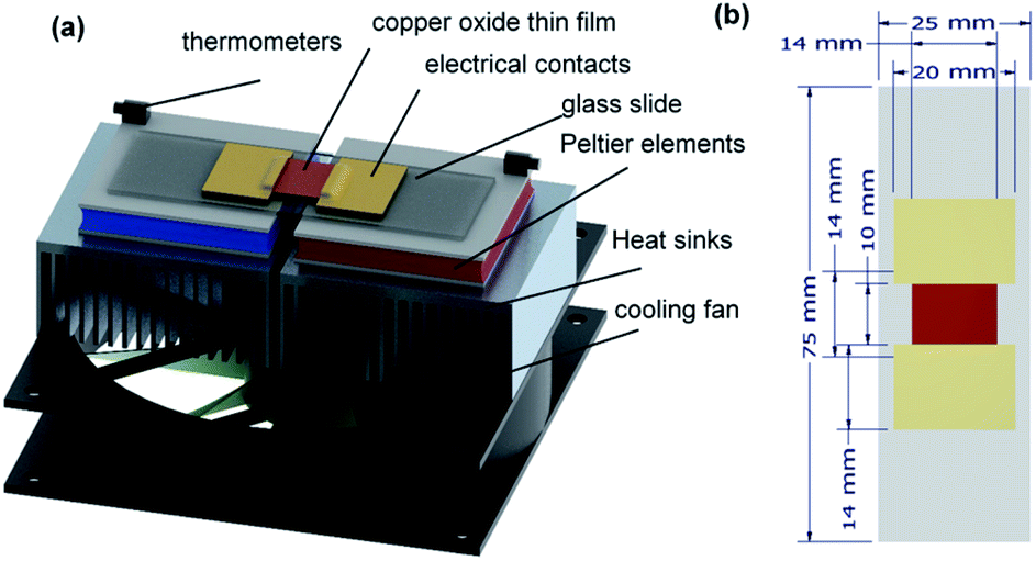 | ||
| Fig. 1 (a) Schematic rendering of the home-made setup employed to characterize the thin-film oxide samples. Wiring has been omitted for clarity. (b) Schematic representation of the deposited thin film. The glass support is depicted in grey, the sample in brown and the golden 20 × 14 mm2 rectangles represent the electrical contacts. | ||
The Seebeck potential was measured using a custom-designed thermoelectric setup (see Fig. 1a for an artistic rendering). The uncertainties were calculated from the standard deviation of three individual measurements, and were consistent with the commonly reported uncertainties of Seebeck coefficients,2 with differences likely due to stochastic variations. The validity of the instrument was previously confirmed through comparison of standard samples with literature data.24,25 The in-plane electrical resistance of the samples was measured using a Fluke 289 multimeter in a 2-point configuration, as previously described.25 Briefly, the multimeter was wired to the two gold–palladium contacts of the copper oxide thin film, depicted in Fig. 1. The electrical conductivity (σ) was calculated using the equation σ = l/(whR), where h is the film thickness (see Table 2), l is the film length (10 mm between the two metal contacts, see Fig. 1b), w is the film width (14 mm, Fig. 1b) and R is the electrical resistance. The crystallographic structure of the films was analysed with X-ray diffraction (XRD) taken on a Bruker D8 Advance Diffractometer using Cu Kα1 radiation (λ = 1.5406 Å). Raman spectroscopy was used for identifying vibration modes in the samples. Raman spectroscopic measurements were performed using a Horiba Jobin Yvon Lab Ram HR800 setup equipped with a CCD detector. Cross-sectional samples were prepared for scanning electron microscopy (SEM) analysis using a JEOL IB-19510 cross-sectional polisher. Secondary electron (SE) and back-scattered electron (BE) signals were acquired using a JEOL JSM-IT300 SEM equipped with a ThermoFisher UltraDry EDS detector. The thickness of the samples was found by varying the acceleration voltage of the SEM and observing the decrease of the substrate EDS signal. Atomic force microscopy (AFM) images were recorded on a Nanosurf Mobile S instrument operating in dynamic force mode. Near edge X-ray absorption fine structure (NEXAFS) analysis of the samples were made on films deposited on Si substrates. For the analysis of the chemical binding state of Cu, the fine structure of the near-edge region of the Cu L3 absorption edge has been measured. The experiments have been performed in fluorescence detection mode at the plane grating monochromator (PGM) beamline58 for undulator radiation, in the laboratory of the Physikalisch Technische Bundesanstalt (PTB) at the electron storage ring BESSY II. The samples are mounted in an ultra-high vacuum chamber.59 A 9-axis goniometer allows precise alignment of the sample and the tuning of the shallow incident angle of the synchrotron radiation to perform (qualitative) depth-resolved measurements.
Results and discussion
Thermoelectric studies
The thermoelectric performance of copper oxide thin films annealed under different atmospheres (air, nitrogen, and oxygen, noted CuO:air, CuO:N, and CuO:O, respectively) has first been investigated by determining their Seebeck coefficient (S) and electrical resistance (R). For this purpose, a temperature gradient was maintained along the sample using two individually controlled Peltier elements and measured by placing an electronic thermometer (DS18B20) at both hot and cold ends (see Fig. 1a). A graph of the measured Seebeck voltage against the temperature difference was plotted for the CuO films annealed under various atmospheres (Fig. 2). The slope of the U versus ΔT plots gives the Seebeck coefficient of the CuO:air, CuO:N and CuO:O films as 175 ± 8 μV K−1, 184 ± 5 μV K−1, and 204 ± 1 μV K−1, respectively. The Seebeck coefficient of the films was found to be positive, confirming the p-type behaviour of copper oxide. The electrical resistance of the CuO:air, CuO:N and CuO:O films were measured in a 2-point configuration, amounting to 6.4, 4.9 and 0.2 MΩ respectively. The CuO:O sample exhibited an excellent electrical conductivity (σ) of 49.6 ± 2.1 S m−1, which is one order of magnitude higher than those of previously reported copper oxide thin films made for sensor applications by Figueira et al.60 This high σ compensates the moderate Seebeck coefficient, resulting in a power factor PF = 2.06 ± 0.09 μW m−1 K−2 comparable to other state-of-the-art thermoelectric copper oxide layers.60 The thermoelectric measurements are summarized in Table 1 below.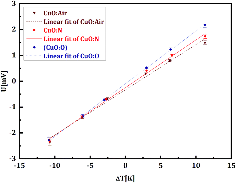 | ||
| Fig. 2 The variation of the Seebeck voltage with the temperature difference for the CuO:air, CuO:N and CuO:O films. | ||
In general, the thin films maintained the high Seebeck coefficient values reported for copper oxides3,35,45,61–65 (see Table 1), comparing favourably with other common thermoelectric materials such as Bi2Te3,66 PbTe,67 and CuAlO2,68 and advanced materials such as Ca3−xBixCo4O9+δ,69 oxides,62,63 and borides,64,65 which makes them ideal for sensing applications. Interestingly, a correlation can be observed in Table 1 between the Seebeck coefficient of the films and their electrical resistance: the film with the highest conductivity (CuO:O) also possesses the highest Seebeck coefficient. This result may at first appear surprising since a higher Seebeck coefficient is typically associated with a decrease in the electrical conductivity for a specific single-phase semiconductor material, when both parameters are controlled by doping. To understand the observed thermoelectric behaviour, we have studied the phases and structure of the films as described in the following.
X-ray diffraction analysis
To rationalize the observed trends in the electrical conductivity and power factor, the structure of the CuO thin films has been next investigated by XRD. Fig. 3 shows the XRD patterns of pure copper oxide films formed on a glass substrate under various annealing conditions. The diffraction peaks observed at 2θ = 38.37 and 65.64° are attributed to the (111) and (022) planes of tenorite with a monoclinic structure, CuO (JCPDS no. 5-0661). For all the samples, the diffraction pattern shows a small reflection at 2θ = 44.62° that has been described in the literature as the (213) plane of paramelaconite (Cu4O3) with tetragonal structure [JCPDS no. 49-1830]. The reflection at 44.62° may also indicate a mixed Cu4O3/Cu2O phase,71 however, no strong reflection could be assigned to the pure Cu2O phase. The co-existence of the phases CuO, Cu4O3 and Cu2O has previously been reported for films created by DC magnetron reactive sputtering by Murali et al.72 and Wang et al.71 The intensity of the (111) orientation is prominent for all our samples, and the annealing atmosphere does not drastically alter the orientation of the CuO phase in the films. The dominating (111) orientation is typical for CuO films when synthesized by thermal oxidation of Cu, or by transformation of a mixed oxide through heat treatment. It has been observed that the oxygen annealing environment can alter the copper oxide phase composition and can induce a transformation to CuO,5 whereas our films still consist of a mix of phases.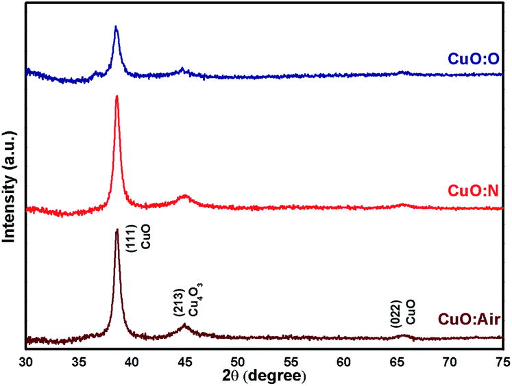 | ||
| Fig. 3 X-ray diffraction profiles of CuO:air, CuO:N and CuO:O samples. | ||
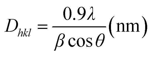
The average crystallite size was estimated from Scherrer's formula given in eqn (1),73,74 where Dhkl is the crystallite size in the direction perpendicular to the lattice planes, hkl are the Miller indices, 0.9 (=K) is a numerical factor known as crystallite-shape factor, λ is the wavelength of the X-ray (1.5406 Å), β is the full width at half maximum of the diffraction reflex at (111), and θ is the diffraction angle. To gain the most accurate result, the dominant (111) reflection was chosen, as this would yield a high signal-to-noise ratio. The other structural parameters such as d-spacing and crystallite size of the prominent 2θ value of CuO films are estimated and listed in Table 2. A similar crystallite size of 12–13 nm was observed for all samples, which indicates that other factors have a more pronounced effect on the electrical conductivity.
 | (1) |
| Sample | d-Spacing (Å) | Crystallite size (nm) | Composition | Thickness (nm) | |
|---|---|---|---|---|---|
| Cu (at%) | O (at%) | ||||
| CuO:air | 2.2327 | 13 | 53.10 ± 0.31 | 46.90 ± 0.39 | 49 ± 2 |
| CuO:N | 2.337 | 13 | 51.94 ± 0.33 | 48.06 ± 0.45 | 44 ± 4 |
| CuO:O | 2.3314 | 12 | 61.20 ± 0.46 | 37.80 ± 0.42 | 72 ± 3 |
Raman spectroscopic analysis
Raman spectroscopy is a good complementary method to determine the film phase structure in the surface vicinity. In this case, the spectra can differentiate between CuO, Cu2O and a mixed copper oxide associated in the literature with paramelaconite (Cu4O3), since they have different Raman active vibrational modes.75 Fig. 4 shows the Raman spectra of the copper oxide thin films previously characterized by XRD in Fig. 3.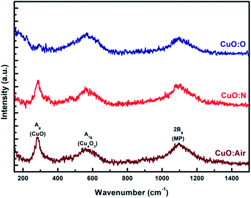 | ||
| Fig. 4 Raman spectra of CuO:air, CuO:N and CuO:O. | ||
CuO has a monoclinic structure with a space group symmetry of C2h6. It has 12 phonon branches: four atoms in the primitive cell (four Cu–O molecules per unit cell and two CuO units in the primitive cell). A factor-group analysis gives the following zone-center modes:
| Γvib = Ag + 2Bg + 4Au + 5Bu | (2) |
There are three acoustic modes (Au + 2Bu), three Raman active modes (Ag + 2Bg) and six infrared active modes (3Au + 3Bu).75 The mixed copper oxide should have a tetragonal crystal structure (space group I41/amd), and their mode is given as:
| Γvib = 3Eg + A1g + 2B1g + 9Eu + 6A2u + 5B2u + 2B1u + 2A1u | (3) |
The Raman spectrum revealed that the phonon modes at 288 cm−1 and 544 cm−1 correspond to the Ag (288 cm−1) band of CuO and A1g (544 cm−1) band of the mixed Cu oxide often referred to as Cu4O3 respectively,72 while the broad band around 500–700 cm−1 indicates a Cu2O phase.71,75 The presence of the CuO, mixed Cu(I)Cu(II) oxide and Cu2O phases is evidenced, and it agrees with the XRD results. In addition to these Raman scattering peaks, it was observed that there was a broadened peak at 1100 cm−1, which is assigned to a multi-phonon (MP) transition.76,77 It has been reported that this band arises due to the anharmonic coupling between phonons in a polar solid. The Raman scattering investigations of the copper oxide thin films show that the oxygen atmosphere has a great effect on the intensity of the bands (Ag) and (A1g).
In both XRD and Raman, the intensity of the CuO peak of CuO:O was weaker than that of the samples CuO:N and CuO:air. Increased intensity means the crystallinity increases and vice versa, which may indicate an uneven distribution of the crystallite size within the CuO:O thin film. In this case, fewer oxygen vacancies may lead to a smaller grain size near the surface, whereas a vacancy-rich inner phase may favour the crystallite reorganization into larger grains.
Chemical analysis by X-ray absorption spectroscopy
To get further information on the Cu oxidation state and thus complement the X-ray diffraction and Raman analysis, near edge X-ray absorption fine structure (NEXAFS) measurements have been conducted. For the NEXAFS measurements, CuO:air has been prepared on a silicon wafer. The silicon wafer was chosen as a substrate due to its flatness and its low concentration of impurities. The sample was prepared with similar sputter parameters as the other samples, but the sputtering time was decreased to get a thinner film with low roughness. Before the NEXAFS experiments, the angular dependent Cu Lα fluorescence intensity was measured to have an insight into the elemental depth profile of Cu and determine the angle of incidence. Four different incident angles (0.8°, 1.5°, 3.4°, and 15°) are chosen and, for each, the energy of the incident radiation is rocked above the Cu L3 absorption edge in steps of 0.25 eV. An energy-dispersive spectrum of each position is recorded for 15 s using a silicon drift detector (SDD). All spectra are deconvolved with PTB's in-house software, using a physical model including scattering background and measured detector response functions of the calibrated SDD.Along with the samples, a CuO and a Cu2O pressed pellet were analysed at 5° incident angle to obtain reference spectra for both oxides. All NEXAFS profiles are corrected regarding self-absorption effects. Assuming that oxygen is homogeneously distributed within the Cu layer, the O Kα fluorescence intensity reflects as a good approximation the qualitative run of the attenuated copper L fluorescence intensity depending on the photon energy. The NEXAFS measurements are shown in the waterfall plot in Fig. 5. With the increasing incident angle, the incident radiation penetrates deeper into the sample, i.e., while the spectrum obtained at 0.8° yields information about the top few nm, at 15° incident angle the whole layer contributes to the measured spectrum. It can be seen that copper(II) oxide is mainly found close to the surface (strong peak at 930.4 eV), and the fraction of Cu(I) increases with depth (peak at 932.8 eV).
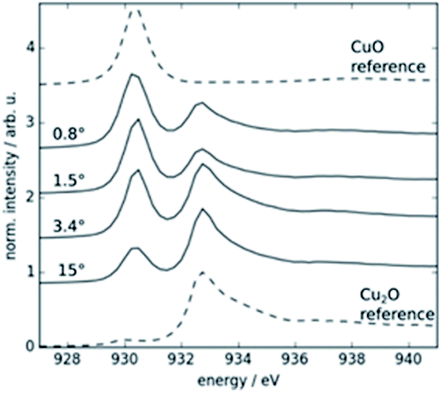 | ||
| Fig. 5 NEXAFS spectra measured of the sample CuO:air at different incidence angles and known Cu oxides.78 | ||
Fig. 5 shows that at the surface (shallow angles) the Cu species resemble more the Cu(II) and at steeper angles, it moves more towards the Cu(I) species. Together with the XRD and Raman studies, we expect a thin surface layer of mixed copper oxide, and with increasing depth, the Cu(II) species and oxygen content are lowered, and the Cu(I) species becomes the predominant species.
Overall, the results indicate that the copper oxide films cannot be described as a simple mixture of copper(I) and (II) species, or as a homogeneous Cu4O3 phase. Instead, the ratio between the copper species varies within the film cross-section, leading most likely to vertical distribution of the charge transport properties and thermopower within the layers.
SEM and AFM analysis
To support our assumptions regarding the composition and morphology of the copper oxide thin films, the samples have been further characterised by SEM and AFM. Fig. 6a shows the SEM cross-section image of CuO:O. It can be noticed that the film cannot be simply identified by the SE contrast due to the smoothly polished surface. The lower density of the glass substrate allows for identifying the film by means of the BE signal, as it can be observed in Fig. 6b. The measured film thickness observed by BE is around 60–70 nm, close to the detection limit of the system. Thus, an alternative method to estimate the film thickness has been used.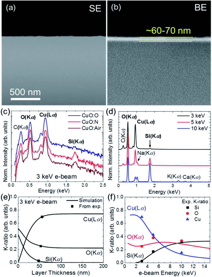 | ||
| Fig. 6 Cross-sectional SEM images of CuO:O sample using (a) secondary electron, and (b) back-scattered electron signal. (c) EDS spectra for all samples measured at 3 keV. (d) EDS spectra measured at 3, 5 and 10 keV for CuO:N sample. (e) Calculated K-ratio for CuO:N at 3 keV e-beam as a function of the layer thickness. Solid squares correspond to the intersection with experimental K-ratio values. (f) Comparison between experimental and calculated K-ratio as a function of the e-beam energy for ∼50 nm CuO layer (sample CuO:air). | ||
In this case, the thickness of the different samples has been calculated by K-ratio analysis from EDS spectra measured at 3, 5 and 10 keV using Stratagem software based on the XPP model proposed by Pouchou,79 which is a non-destructive and straightforward method to estimate single or multilayer film thickness, and therefore simplifies the sample preparation.
For simplicity, we have assumed a constant film (CuO) and substrate (SiO2) densities using the Cu/O composition (summarized in Table 2) quantified from EDS spectra measured at 3 keV, shown in Fig. 6c. Note that at 3 keV the Si(Kα) signal at 1.74 keV from CuO:O sample is negligible compared to that measured on CuO:N and CuO:air, which indicates that CuO:O film is thicker. Fig. 6d shows the EDS spectra (normalized in respect to the total intensity) measured at 3, 5 and 10 keV from the sample CuO:N where the peak intensities of the O(Kα), Cu(Lα) and Si(Kα) vary as a function of the e-beam energy, and thus the K-ratio. Carbon at the surface as well as Na, K and Ca elements from the glass substrate are included for reference in Fig. 6d. As an example, Fig. 6e shows the calculated K-ratio as a function of the film thickness for 3 keV e-beam. Dark squares in Fig. 6e correspond to the intersection of the experimental K-ratio with the calculated curves resulting in an estimated film thickness of ∼50 nm. Similarly, Fig. 6f shows the calculated K-ratio as a function of the e-beam energy for the estimated film thickness showing a good agreement with experimental values measured at 3, 5 and 10 keV. Following a similar procedure, we have estimated the sample thicknesses summarized in Table 2. It is important to note that sample CuO:O is in good agreement with the film thickness observed by BE in Fig. 6b.
AFM images shown in Fig. 7a–c reveal that most copper oxide particles have sizes between 10–50 nm for all samples, which is consistent with the smaller crystallite size expected from the Raman spectroscopy and XRD data. By combining this information with the insights gained from the XRD, SEM, EDS and NEXAFS analysis, an illustrative model is proposed in Fig. 7d for the cross-film morphology. Accordingly, the films present a vertical transition between the Cu(I) and Cu(II) oxide species. The CuO:O film is thicker and has a smaller relative oxygen content, which may indicate that it has a larger amount of Cu(I) oxide in its composition, beneath the surface (Table 2). This may explain its improved Seebeck coefficient and electrical conductivity, as Cu2O often displays higher S and σ values than CuO.35,60
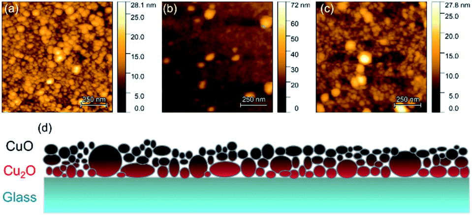 | ||
| Fig. 7 (a–c) AFM images of the copper oxide samples: (a) CuO:air, (b) CuO:N, (c) CuO:O. (d) Model of the morphology and species distribution within the copper oxide films, based on the XRD, Raman, AFM, SEM and NEXAFS data. | ||
Conclusions
CuO thin films have been obtained through a simple fabrication method (oxidation of Cu metallic film deposited by sputtering), to investigate their potential for thermoelectric sensing applications. We have studied the influence of post deposition annealing in oxygen, air and nitrogen ambient. All samples showed the presence of CuO, mixed Cu(I)/Cu(II) oxide and Cu2O phases with contributions varying in depth in the film. All samples showed a p-type character. The copper oxide sample annealed under an oxygen atmosphere exhibited a high Seebeck coefficient of 204 μV K−1 and electrical conductivity of 50 S m−1. To the best of our knowledge, these values represent the state of the art for CuO thin films with a mixed copper oxide phase, which are prepared by simple sputtering deposition without any additional dopants. Although further improvements of the thermoelectric values are still required for energy harvesting applications, the films may be easily employed for temperature sensors due to their high Seebeck coefficients. The insights gained from these mixed-phase films may further help in understanding the Seebeck coefficient and electrical conductivity of multi-component oxide systems.Conflicts of interest
There are no conflicts to declare.Acknowledgements
This work was carried out with the financial support from DST-DAAD through the sanctioned research project no. DST/INT/FRG/DAAD/P-29/2017 dated 20.06.2017. C. A. thanks to DST-Inspire for financial assistance through a fellowship. K. B. is most grateful for the scholarship from the International Max-Planck Research School at the Fritz Haber Institute. V. A. is most grateful to the Gesellschaft Deutscher Chemiker for the August-Wilhelm-von-Hofmann Scholarship and to the German Federal Government and the Bayer Foundations for the “Deutschlandstipendium” scholarship. J. B. would like to thank the Excellence Initiative of the Deutsche Forschungsgemeinschaft for financial support. The authors are thankful to Prof. Robert Schlögl for helpful discussions on the copper oxide mixed phases. The Research Council of Norway is gratefully acknowledged for the support to the Norwegian Micro- and Nano-Fabrication Facility, NorFab (project no. 245963) and FUNDAMeNT (project no. 251131).References
- M. S. Dresselhaus, G. Chen, M. Y. Tang, R. G. Yang, H. Lee, D. Z. Wang, Z. F. Ren, J. P. Fleurial and P. Gogna, Adv. Mater., 2007, 19, 1043–1053 CrossRef CAS.
- G. J. Snyder and E. S. Toberer, Nat. Mater., 2008, 7, 105–114 CrossRef CAS PubMed.
- V. Andrei, K. Bethke and K. Rademann, Energy Environ. Sci., 2016, 9, 1528–1532 RSC.
- I. Petsagkourakis, K. Tybrandt, X. Crispin, I. Ohkubo, N. Satoh and T. Mori, Sci. Technol. Adv. Mater., 2018, 19, 836–862 CrossRef CAS PubMed.
- C. Dagdeviren, Z. Li and Z. L. Wang, Annu. Rev. Biomed. Eng., 2017, 19, 85–108 CrossRef CAS PubMed.
- T. Mori and S. Priya, MRS Bull., 2018, 43, 176–180 CrossRef.
- A. Miozzo, S. Boldrini, A. Ferrario and M. Fabrizio, J. Nanosci. Nanotechnol., 2017, 17, 1601–1607 CrossRef CAS PubMed.
- N. R. Kristiansen and H. K. Nielsen, J. Electron. Mater., 2010, 39, 1746–1749 CrossRef CAS.
- S. Skarvelis-Kazakos, P. Papadopoulos, I. G. Unda, T. Gorman, A. Belaidi and S. Zigan, Appl. Energy, 2016, 167, 323–335 CrossRef.
- F. Frobenius, G. Gaiser, U. Rusche and B. Weller, J. Electron. Mater., 2016, 45, 1433–1440 CrossRef CAS.
- B. Orr, A. Akbarzadeh, M. Mochizuki and R. Singh, Appl. Therm. Eng., 2016, 101, 490–495 CrossRef.
- D. M. Rowe, Appl. Energy, 1991, 40, 241–271 CrossRef CAS.
- P. S. Cooper, Astropart. Phys., 2009, 31, 267–269 CrossRef.
- T. C. Holgate, R. Bennett, T. Hammel, T. Caillat, S. Keyser and B. Sievers, J. Electron. Mater., 2015, 44, 1814–1821 CrossRef CAS.
- S. G. MacDonald, Biothermal power source for implantable devices, US Pat., 20080200968A1, 2008.
- D. Bhatia, S. Bairagi, S. Goel and M. Jangra, J. Pharm. Bioallied Sci., 2010, 2, 51–54 CrossRef PubMed.
- D. Champier, Energy Convers. Manage., 2017, 140, 167–181 CrossRef.
- V. Andrei, R. L. Z. Hoye, M. Crespo-Quesada, M. Bajada, S. Ahmad, M. De Volder, R. Friend and E. Reisner, Adv. Energy Mater., 2018, 8, 1801403 CrossRef.
- S. Julich, M. Riedel, M. Kielpinski, M. Urban, R. Kretschmer, S. Wagner, W. Fritzsche, T. Henkel, R. Moller and S. Werres, Biosens. Bioelectron., 2011, 26, 4070–4075 CrossRef CAS PubMed.
- W. Liu, J. Hu, S. Zhang, M. Deng, C.-G. Han and Y. Liu, Mater. Today Phys., 2017, 1, 50–60 CrossRef.
- T. Mori, Small, 2017, 13, 1702013 CrossRef PubMed.
- J. Mao, Z. Liu, J. Zhou, H. Zhu, Q. Zhang, G. Chen and Z. Ren, Adv. Phys., 2018, 67, 69–147 CrossRef.
- C. Bianchi, J. Loureiro, P. Duarte, J. Marques, J. Figueira, I. Ropio and I. Ferreira, Adv. Mater. Technol., 2016, 1, 1–6 Search PubMed.
- V. Andrei, K. Bethke, F. Madzharova, A. C. Bronneberg, J. Kneipp and K. Rademann, ACS Appl. Mater. Interfaces, 2017, 9, 33308–33316 CrossRef CAS PubMed.
- V. Andrei, K. Bethke, F. Madzharova, S. Beeg, A. Knop-Gericke, J. Kneipp and K. Rademann, Adv. Electron. Mater., 2017, 3, 1600473 CrossRef.
- E. A. Mondarte, V. Copa, A. Tuico, C. J. Vergara, E. Estacio, A. Salvador and A. Somintac, Mater. Sci. Semicond. Process., 2016, 45, 27–31 CrossRef CAS.
- B. Hinterleitner, I. Knapp, M. Poneder, Y. Shi, H. Müller, G. Eguchi, C. Eisenmenger-Sittner, M. Stöger-Pollach, Y. Kakefuda, N. Kawamoto, Q. Guo, T. Baba, T. Mori, S. Ullah, X.-Q. Chen and E. Bauer, Nature, 2019, 576, 85–90 CrossRef CAS PubMed.
- K. Bethke, V. Andrei and K. Rademann, PLoS One, 2016, 11, e0151708 CrossRef PubMed.
- B. C. Jeon, S. M. Yang and S. C. Chae, Curr. Appl. Phys., 2017, 17, 684–687 CrossRef.
- H. Yoshiyama, S. Tanaka, Y. Mikami, S. Ohshio, J. Nishiura, H. Kawakami and H. Kobayashi, J. Cryst. Growth, 1988, 86, 56–60 CrossRef CAS.
- K. Oura, M. Katayama, A. V. Zotov, V. G. Lifshits and A. A. Saranin, in Surface Science, 2003, ch. 14, pp. 357–387, DOI:10.1007/978-3-662-05179-5_14.
- V. F. Mitin, V. K. Lazarov, L. Lari, P. M. Lytvyn, V. V. Kholevchuk, L. A. Matveeva, V. V. Mitin and E. F. Venger, Thin Solid Films, 2014, 550, 715–722 CrossRef CAS.
- D. M. Mattox, J. Vac. Sci. Technol., A, 1989, 7, 1105–1114 CrossRef CAS.
- M. D. Thouless, Acta Metall. Mater., 1993, 41, 1057–1064 CrossRef CAS.
- S. Walia, S. Balendhran, H. Nili, S. Zhuiykov, G. Rosengarten, Q. H. Wang, M. Bhaskaran, S. Sriram, M. S. Strano and K. Kalantar-zadeh, Prog. Mater. Sci., 2013, 58, 1443–1489 CrossRef CAS.
- S. H. A. Ahmad, M. F. Al-Kuhaili, S. M. A. Durrani, M. M. Faiz and A. Ul-Hamid, Sol. Energy Mater. Sol. Cells, 2017, 169, 258–263 CrossRef CAS.
- M. F. Al-Kuhaili, S. H. A. Ahmad, S. M. A. Durrani, M. M. Faiz and A. Ul-Hamid, Mater. Sci. Semicond. Process., 2015, 39, 84–89 CrossRef CAS.
- M. F. Al-Kuhaili, S. H. A. Ahmad, S. M. A. Durrani, M. M. Faiz and A. Ul-Hamid, Mater. Des., 2015, 73, 15–19 CrossRef CAS.
- M. F. Al-Kuhaili, Vacuum, 2008, 82, 623–629 CrossRef CAS.
- T. M. Tritt and M. A. Subramanian, MRS Bull., 2006, 31, 188–194 CrossRef.
- Y. Feng, X. Jiang, E. Ghafari, B. Kucukgok, C. Zhang, I. Ferguson and N. Lu, Adv. Compos. Hybrid Mater., 2017, 1, 114–126 CrossRef.
- K. S. Khashan, M. S. Jabir and F. A. Abdulameer, J. Phys.: Conf. Ser., 2018, 1003, 012100 CrossRef.
- S. Choudhary, J. V. N. Sarma, S. Pande, S. Ababou-Girard, P. Turban, B. Lepine and S. Gangopadhyay, AIP Adv., 2018, 8, 055114 CrossRef.
- D. S. Murali and A. Subrahmanyam, J. Phys. D: Appl. Phys., 2016, 49, 375102 CrossRef.
- V. Andrei, K. Bethke and K. Rademann, Appl. Phys. Lett., 2014, 105, 233902 CrossRef.
- S. Anandan, X. Wen and S. Yang, Mater. Chem. Phys., 2005, 93, 35–40 CrossRef CAS.
- M. J. Jing, Z. Y. Ding, H. S. Hou, Y. Zhang, G. Q. Zou, S. M. Li and X. B. Ji, Chem. Phys. Lett., 2016, 653, 30–34 CrossRef CAS.
- K. Bethke, S. Palantöken, V. Andrei, M. Roß, V. S. Raghuwanshi, F. Kettemann, K. Greis, T. T. K. Ingber, J. B. Stückrath, S. Valiyaveettil and K. Rademann, Adv. Funct. Mater., 2018, 28, 1800409 CrossRef.
- X. L. Gou, G. X. Wang, J. S. Yang, J. Park and D. Wexler, J. Mater. Chem., 2008, 18, 965–969 RSC.
- C.-T. Hsieh, J.-M. Chen, H.-H. Lin and H.-C. Shih, Appl. Phys. Lett., 2003, 83, 3383–3385 CrossRef CAS.
- W.-W. Wang, W.-Z. Yu, P.-P. Du, H. Xu, Z. Jin, R. Si, C. Ma, S. Shi, C.-J. Jia and C.-H. Yan, ACS Catal., 2017, 7, 1313–1329 CrossRef CAS.
- M. T. Greiner, T. E. Jones, B. E. Johnson, T. C. R. Rocha, Z. J. Wang, M. Armbrüster, M. Willinger, A. Knop-Gericke and R. Schlögl, Phys. Chem. Chem. Phys., 2015, 17, 25073–25089 RSC.
- V. Andrei, K. Bethke and K. Rademann, Phys. Chem. Chem. Phys., 2016, 18, 10700–10707 RSC.
- Y. Wang, J. Ghanbaja, F. Soldera, S. Migot, P. Boulet, D. Horwat, F. Mücklich and J. F. Pierson, Appl. Surf. Sci., 2015, 335, 85–91 CrossRef CAS.
- L. Zhao, H. Chen, Y. Wang, H. Che, P. Gunawan, Z. Zhong, H. Li and F. Su, Chem. Mater., 2012, 24, 1136–1142 CrossRef CAS.
- H.-S. Kim, M. D. Kumar, W.-H. Park, M. Patel and J. Kim, Sens. Actuators, A, 2017, 253, 35–40 CrossRef CAS.
- M. Das, C. Bittencourt, J. J. Pireaux and S. A. Shivashankar, Appl. Phys. A: Mater. Sci. Process., 2012, 109, 245–254 CrossRef CAS.
- F. Senf, U. Flechsig, F. Eggenstein, W. Gudat, R. Klein, H. Rabus and G. Ulm, J. Synchrotron Radiat., 1998, 5, 780–782 CrossRef CAS PubMed.
- J. Lubeck, B. Beckhoff, R. Fliegauf, I. Holfelder, P. Honicke, M. Muller, B. Pollakowski, F. Reinhardt and J. Weser, Rev. Sci. Instrum., 2013, 84, 045106 CrossRef CAS PubMed.
- J. Figueira, J. Loureiro, J. Marques, C. Bianchi, P. Duarte, M. Ruoho, I. Tittonen and I. Ferreira, ACS Appl. Mater. Interfaces, 2017, 9, 6520–6529 CrossRef CAS PubMed.
- Y. Hirose, M. Tsuchii, K. Shigematsu, Y. Kakefuda, T. Mori and T. Hasegawa, Appl. Phys. Lett., 2019, 114 Search PubMed.
- P. Mele, S. Saini, H. Honda, K. Matsumoto, K. Miyazaki, H. Hagino and A. Ichinose, Appl. Phys. Lett., 2013, 102, 253903 CrossRef.
- I. Sinnarasa, Y. Thimont, L. Presmanes, A. Barnabé and P. Tailhades, J. Appl. Phys., 2018, 124, 165306 CrossRef.
- T. Tynell, T. Aizawa, I. Ohkubo, K. Nakamura and T. Mori, J. Cryst. Growth, 2016, 449, 10–14 CrossRef CAS.
- G. Guélou, M. Martirossyan, K. Ogata, I. Ohkubo, Y. Kakefuda, N. Kawamoto, Y. Kitagawa, J. Ueda, S. Tanabe, K. Maeda, K. Nakamura, T. Aizawa and T. Mori, Materialia, 2018, 1, 244–248 CrossRef.
- Y. Zhang, C. L. Hapenciuc, E. E. Castillo, T. Borca-Tasciuc, R. J. Mehta, C. Karthik and G. Ramanath, Appl. Phys. Lett., 2010, 96, 062107 CrossRef.
- K. Kishimoto, M. Tsukamoto and T. Koyanagi, J. Appl. Phys., 2002, 92, 5331–5339 CrossRef CAS.
- H. Kawazoe, M. Yasukawa, H. Hyodo, M. Kurita, H. Yanagi and H. Hosono, Nature, 1997, 389, 939–942 CrossRef CAS.
- S. Li, R. Funahashi, I. Matsubara, K. Ueno, S. Sodeoka and H. Yamada, Chem. Mater., 2000, 12, 2424–2427 CrossRef CAS.
- D. Hartung, F. Gather, P. Hering, C. Kandzia, D. Reppin, A. Polity, B. K. Meyer and P. J. Klar, Appl. Phys. Lett., 2015, 106, 253901 CrossRef.
- Y. Wang, J. Ghanbaja, S. Bruyère, F. Soldera, D. Horwat, F. Mücklich and J. F. Pierson, Sci. Rep., 2017, 7, 11122 CrossRef CAS PubMed.
- D. S. Murali and S. Aryasomayajula, Appl. Phys. A: Mater. Sci. Process., 2018, 124 Search PubMed.
- U. Holzwarth and N. Gibson, Nat. Nanotechnol., 2011, 6, 534 CrossRef CAS PubMed.
- P. Scherrer, in Kolloidchemie Ein Lehrbuch, Springer, 1912, pp. 387–409 Search PubMed.
- L. Debbichi, M. C. Marco de Lucas, J. F. Pierson and P. Krüger, J. Phys. Chem. C, 2012, 116, 10232–10237 CrossRef CAS.
- J. C. Irwin, J. Chrzanowski, T. Wei, D. J. Lockwood and A. Wold, Phys. C, 1990, 166, 456–464 CrossRef CAS.
- W. Wang, Q. Zhou, X. Fei, Y. He, P. Zhang, G. Zhang, L. Peng and W. Xie, CrystEngComm, 2010, 12, 2232–2237 RSC.
- J. Baumann, Advanced X-ray analytical methods for the characterization of buried interfaces with relevance for energy conversion devices, Doctoral Thesis, 2017 DOI:10.14279/depositonce-6581.
- J.-L. Pouchou, Anal. Chim. Acta, 1993, 283, 81–97 CrossRef CAS.
Footnote |
| † Both authors contributed equally. |
| This journal is © The Royal Society of Chemistry 2020 |