
 Open Access Article
 This Open Access Article is licensed under a Creative Commons Attribution-Non Commercial 3.0 Unported Licence
One-step electrosynthesis of visible light responsive double-walled alloy titanium dioxide nanotube arrays for use in photocatalytic degradation of dibutyl phthalate†
Yuan Wanga,
Xueke Zhanga,
Suzhen Youa and
Yun Hu *abc
*abc
aSchool of Environment and Energy, South China University of Technology, Guangzhou 510006, P. R. China. E-mail: huyun@scut.edu.cn; Tel: +86-20-3938-0573
bGuangdong Provincial Key Laboratory of Atmospheric Environment and Pollution Control, Guangzhou 510006, P. R. China
cThe Key Lab of Pollution Control and Ecosystem Restoration in Industry Clusters, Ministry of Education, Guangzhou 510006, P. R. China
First published on 3rd June 2020
Abstract
Using Ti-6Al-4V (TC4) alloy as a substrate, double-walled alloy titanium dioxide nanotube arrays (DW-ATNTAs) with a special porous inner wall and visible light response are synthesized in situ by an improved anodization method. During the anodization, the V element in the TC4 alloy converts into V2O5 which dominates the visible light response of DW-ATNTAs. After 3 h of irradiation with visible light, there is a nearly 97% reduction of dibutyl phthalate (DBP) by DW-ATNTAs in which the degradation kinetic constant is 50 and 7 times higher than that of titanium dioxide nanotube arrays (TNTAs) and alloy titanium dioxide layers (A-TiO2(plate)), respectively. The richly porous inner wall structure of DW-ATNTAs can provide sufficient vacancies for adsorption and active sites for photocatalytic reaction. Furthermore, the differences in the morphology of the inner and outer walls are attributed to the thicker carbon and fluorine-rich oxide layer (C, F-rich oxide layer) resulting from a longer time that the inner wall spends in contact with the electrolyte during the anodization process. This special porous inner wall structure was formed due to the anti-corrosion properties of the alloy caused by appropriate amounts of V and Al as well as the removal of C and F elements during the calcination process.
1. Introduction
Environmental pollution and energy shortage are two major problems that urgently need to be solved in the 21st century. In 1972, Fujishima reported that TiO2 can be used to split water into hydrogen and oxygen when irradiated with ultraviolet light, demonstrating the utility of photocatalysis in dealing with important energy and environmental problems.1 Shortly thereafter, in 1976, Schurr employed TiO2 in the photocatalytic degradation of polychlorinated biphenyls (PCBs), thereby successfully applying photocatalytic materials in the field of environmental purification.2 Comparing with more conventional water treatment technologies, photocatalytic oxidation technology can use sunlight as the principal energy source, operating under simpler and milder conditions.3–8 Therefore, TiO2 photocatalytic oxidation technology is widely recognized as a green and highly effective technique that can be used to solve environmental problems in a cost-effective manner.9Many applications of this technology utilize nanoparticles of TiO2 to maximize the active sites on the surface of the material. However, the small size of nanoparticles is also a disadvantage because photo-generated electrons and holes cannot separate very far, therefore, the pair often recombine before being productively utilized in the common photocatalysis process.10–12 Actually, the lifetime of a photo-generated h+ is enough to migrate by random walk over a distance of several hundred nanometers to several micrometers from the location on the surface where it is originated.13 This length is quite comparable to the inner dimensions of TiO2 nanotubes, which indicates that replacing the TiO2 nanoparticles with a nano-tubular layer can particularly effective in reducing the frequency of unproductive recombination.14
Over the past decade, various morphologies of TiO2 nanotubes have been developed, such as bamboo-like15 and Y-branched,16 owed to their favorable properties, such as high surface area, enhanced mass transport and increased rate of diffusion. Comparing with traditional nanotubes, specially-shape nanotubes have more adsorption and catalytic active sites, thus exhibiting higher catalytic performance and are gradually becoming the focus of research. TiO2 nanotubes can be prepared by hydrothermal methods,17,18 template methods,19,20 sol gel methods21,22 and anodization methods.23,24 Irregular nanotube structures (single tubes/bundles of tube/loose agglomerates of tubes) are more easily formed through methods that use solution-based and template-based titanium precursors. In contrast, regular and ordered TiO2 nanotube arrays can be prepared on a Ti substrate through anodization methods that provide a directed (ideally one-dimensional) electron transfer path. The diameter and length of the tube, as well as the thickness of the wall, are quite controllable. Furthermore, the nanotube arrays, being attached to the metal substrate surface, are easy to handle, which avoids the problems of the immobilization and cycle of powders. However, photocatalytic technology is limited by the UV/Vis light response range and low quantum efficiency of TiO2. Moreover, the existing modification technology for TiO2 nanotube arrays (TNTAs), such as metal/non-metallic ion doping,25–29 and hollow core–shell CdS sensitization30 is complicated and not easily controlled. As a result, in practice, most prepared nanotube arrays have weak responses and cannot meet the needs of industrial production.
Therefore, finding a simple and fast method to prepare nanotube arrays with the adequate response in the visible light range, controllable morphology, enhance mass transportation and directed electronic transmission is an important goal for advanced environmental pollution treatment technology. In order to solve this problem, the self-ordering anodization, which is based on Ti alloys substrate, is proposed as a method for forming highly regular composite oxide nanotube arrays. For example, Macak introduced the TiO2-based composite oxide nanotube arrays on the surface of Ti-6Al-7Nb alloys by anodization.31 Recent studies show that nanotube arrays were successful fabricated on the surface of Ti-6Al-4V,32 Ti-35Nb-5Ta-7Zr,33 Ti-15Mo,34 Ti-Al,35 Ti-28Zr-8Nb,36 Ti-13Nb-13Zr37 and other alloys, which were employed in a range of fields, such as biomedicine,38 gas sensors39 and photocatalytic water splitting. Allam et al. reported that nanotube arrays prepared on the surface of Ti-Nb-Zr alloy had 17.5% higher photo-response ability than nanotube arrays synthesized on the surface of Ti, when exposed to 320–400 nm UV light.40 However, there are only a few applications of composite oxide nanotube arrays in the field of water treatment, and the catalytic mechanism in those cases has not yet been clearly reported.
TC4 (Ti-6Al-4V) alloy is the most widely known titanium alloy, which has evenly distributed Ti, Al and V element. Because of its commercial availability and stability, TC4 is widely employed as 3D printing41 and biological applications42 and is the focus of this study, also. The preparation of nanotube arrays and the visible semiconductor composite were synchronously realized through an improved anodization. The visible light photocatalytic performance of the arrays was investigated by the photo-degradation of non-biodegradability dibutyl phthalate (DBP).43 The anodic conditions, such as voltage, reaction time and electrolyte ratio, resulted in the difference of morphologies of photocatalysts, were also discussed. The mechanism of DBP degradation using these photocatalysts with different morphologies under visible light irradiation was investigated. Finally, a schematic diagram was developed to illustrate the formation mechanism of double-walled nanotube arrays.
2. Experimental
2.1 Preparation of materials
2.2 Characterizations
The scanning electron microscopy images were taken by field emission scanning electron microscopy (SEM, Merlin, ZEISS Co., Germany). Transmission electron microscopy (TEM, JEM-2100F, JEOL Co., Japan) analyses were performed to characterize the morphology of the samples, and the applied acceleration voltages of TEM and HRTEM were both 200 kV. In order to determine the distribution of elements in the products, energy dispersive spectrum (EDS) and the EDS mapping image were obtained using TEM and HRTEM, respectively. The surface areas were measured using a Builder 4200 instrument (ASAP 2020M, Micromeritics Co., USA) with the Brunauer–Emmett–Teller method. The X-ray powder diffraction (XRD) measurement of the samples was performed on a Bruker D8 Advance with graphite monochromatic Cu Kα radiation (λ = 1.541874 Å). The X-ray photoelectron spectroscopy (XPS, Axis Ultra DLD, Kratos Inc., England) was employed to investigate the chemical compositions of the constituent elements. Diffuse reflectance spectra were measured using a UV-Vis spectrophotometer (UV-2550, Shimadzu Co., Japan), and BaSO4 was used as the reflectance standard. The i–t curve was obtained using a homemade three-electrode system on an electrochemical workstation (CHI660E, CH Instruments Ins., USA) with an electrolyte of 0.5 mol L−1 Na2SO4. Ag/AgCl (KCl, 3 mol L−1) and a Pt wire were used as the reference electrode and the counter electrode, respectively.2.3 Photocatalytic performance test
The photocatalytic experiments were carried out using a self-made reactor (Fig. S1†). In each case, the alloy tablet catalyst was suspended by a support frame in 100 mL of solutions containing 5 mg L−1 of DBP. A 300 W xenon lamp which had an intensity of 100 mW cm−2 with a UV cut-off filter was used as a light source. Before the light was turned on, the solution was kept in darkness for 60 min to achieve adsorption and desorption equilibration of pollutants on the catalyst. At specified time intervals, 10 mL of samples were taken from the reactor and filtered through a 0.45 μm membrane filter. The concentration of DBP was determined by a high performance liquid chromatography (Shimadzu LC 20AT), equipped with an HC-C18 column (250 × 4.6 mm i.d., 5 μm, Thermo Scientific). The mobile phase was a mixture of methanol and water (90![[thin space (1/6-em)]](https://www.rsc.org/images/entities/char_2009.gif) :10, v/v), flowing at a rate of 1.0 mL min−1. The UV detector was operated at 228 nm.
:10, v/v), flowing at a rate of 1.0 mL min−1. The UV detector was operated at 228 nm.
The stability and reusability of the catalysts were investigated by repeating the adsorption and degradation process for DBP. After each process of photocatalytic degradation, the catalyst was separated and re-activated by heating at 300 °C in air for 3–6 h. Subsequently, it was reused in the same concentration of DBP solution.
3. Results and discussion
3.1 The optimal conditions of preparation for DW-ATNTAs
Anodization conditions, such as voltage, reaction time and electrolyte ratio, have a great influence on the morphology and property of nanotube arrays. Therefore, in order to synthesize nanotube arrays on TC4 with optimal photocatalytic performance, a series of single factor experiments were designed to explore the effects of voltage, reaction time and electrolyte ratio. The condition optimization experiment was evaluated by the photocatalytic degradation of DBP under visible light. Results of SEM, XRD, UV-Vis DRS, i–t curve and photocatalytic performance are shown in Fig. S2–S5† and summarized in Table 1.| Anodizing condition | Double-walled structure | Inner diameter/nm | Outer diameter/nm | Inner wall thickness/nm | Outer wall thickness/nm | Maximum light response wavelength/nm | DBP removal efficiency/% |
|---|---|---|---|---|---|---|---|
| 30 V-2 h-0.5 wt% NH4F-2 vol% H2O | ✗ | — | 140 | — | 10 | 465 | 47.19 |
| 50 V-2 h-0.5 wt% NH4F-2 vol% H2O | ✗ | — | 160 | — | 15 | 505 | 49.69 |
| 70 V-2 h-0.5 wt% NH4F-2 vol% H2O | ✓ | 150 | 180 | 15 | 15 | 605 | 73.12 |
| 90 V-2 h-0.5 wt% NH4F-2 vol% H2O | ✗ | — | 200 | — | 40 | 545 | 59.01 |
| 70 V-1 h-0.5 wt% NH4F-2 vol% H2O | ✗ | — | 180 | — | 10 | 515 | 39.39 |
| 70 V-3 h-0.5 wt% NH4F-2 vol% H2O | ✓ | 100 | 180 | 20 | 20 | 607 | 96.42 |
| 70 V-4 h-0.5 wt% NH4F-2 vol% H2O | ✗ | — | 180 | — | 50 | 555 | 30.75 |
| 70 V-3 h-0.3 wt% NH4F-2 vol% H2O | ✗ | — | 180 | — | 20 | 460 | 69.96 |
| 70 V-3 h-0.7 wt% NH4F-2 vol% H2O | ✗ | — | 180 | — | 20 | 525 | 85.33 |
| 70 V-3 h-0.5 wt% NH4F-1 vol% H2O | ✗ | — | 180 | — | 30 | 580 | 86.10 |
| 70 V-3 h-0.5 wt% NH4F-3 vol% H2O | ✓ | 150 | 180 | 15 | 15 | 590 | 62.89 |
These data show that the optimal anodization conditions of nanotube arrays are a voltage of 70 V, for 3 h, and using a 0.5 wt% NH4F–2 vol% H2O electrolyte, which produce the best performing double-walled alloy titanium dioxide nanotube arrays (DW-ATNTAs). The sample generated under this optimal condition successfully degraded nearly 97% of DBP after 3 h of irradiation under visible light. The SEM images (Fig. S5c and d†), shows that a double-walled alloy-based nanotube arrays are successfully synthesized. The XRD analysis (Fig. S5g†) shows that DW-ATNTAs are in an anatase phase. The UV-Vis DRS (Fig. S5i†) and i–t curve (Fig. S5h†) show that the photo-response range of DW-ATNTAs is successfully broadened to 607 nm with stable photocurrent response capability. In addition, comparing with the strong acid and corrosive reagents have reported in the existing literature,46,47 the reagents used in this method are all low-toxicity and low-harm. And the preparation process without generating pungent smell and strong acid waste liquid is milder so that less secondary pollution was produced.
3.2 Characteristics of the photocatalysts
The morphologies and pore structure of the photocatalysts are analyzed by SEM and N2 adsorption/desorption isotherm, with the results shown in Fig. 1. A-TiO2(plate) signifies an oxide layer of TC4 alloy, a model of which is depicted in Fig. 1d. Fig. 1a and b shows that the surface of the oxide layer is rough and there is no nanotube array generate. Fig. 1c show that the isotherm of A-TiO2(plate) is Type III, indicating that there is no pore structure on the surface, which is consistent with the SEM characterization.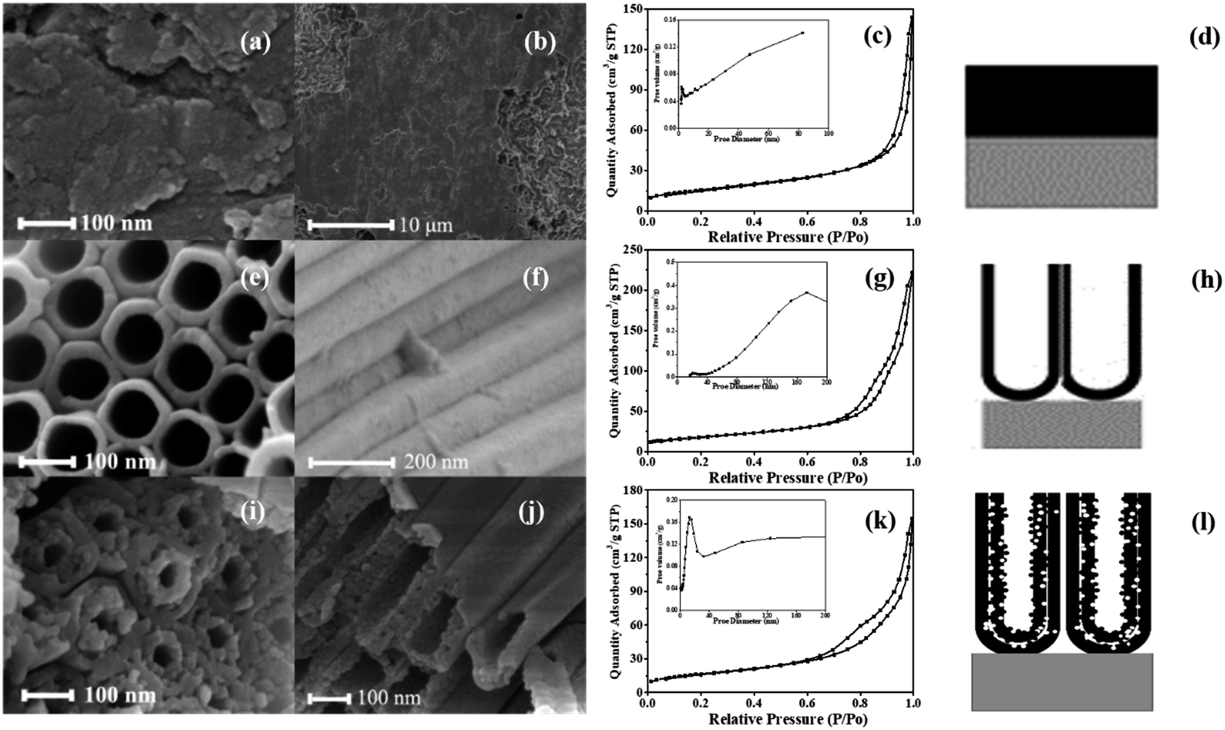 | ||
| Fig. 1 The (a) details and (b) large-scale surface SEM images, (c) N2 adsorption/desorption isotherm with inset of pore size distribution and (d) model diagram of A-TiO2(plate); (e) top and (f) lateral view SEM images, (g) N2 adsorption/desorption isotherm with inset of pore size distribution and (h) model diagram of SW-TNTAs; (i) top and (j) lateral view SEM images, (k) N2 adsorption/desorption isotherm with inset of pore size distribution and (l) model diagram of DW-ATNTAs. | ||
Single-walled titanium dioxide nanotube arrays (SW-TNTAs) are prepared on Ti. Fig. 1e and f are the top and lateral views of the SW-TNTAs, with a diameter of 120 nm and a wall thickness of 15 nm. The isotherm of sample is Type III with an H3 hysteresis loop (Fig. 1g), indicating that the SW-TNTAs has a large pore structure, with the pore diameters generally in the range of 160–200 nm; i.e., the tube diameter. The model diagram of SW-TNTAs is shown in Fig. 1h.
The top and lateral views of the DW-ATNTAs in Fig. 1i and j clearly shows that double-walled nanotube arrays are fabricated. In the existing literature, the inner and outer walls of double-walled TiO2 nanotube are all smooth surfaces,48–50 but this method obtained a special double-walled structure with smooth outer walls and porous inner walls. The outer wall is relatively smooth with the diameter of 180 nm and the thickness of 20 nm, while the inner wall is porous with a diameter of 100 nm and the thickness of 20 nm. The isotherm of DW-ATNTAs is Type III with H3 + H2 hysteresis loop (Fig. 1k), which show that DW-ATNTAs contain two pore structures in the range of 15–20 nm and >50 nm, corresponding to the mesopores and macropores respectively. Combining with SEM results, the porous inner wall is found to be a mesoporous structure. The lateral and bottom views of the DW-ATNTAs are shown in Fig. 2. The thickness of the oxide layer on TC4 is about 12.61 μm. The bottom view (Fig. 2b) clearly show the double-walled structure, including the porous inner wall, indicating that DW-ATNTAs has a uniform morphology. The corresponding model diagram of DW-ATNTAs is shown in Fig. 1l.
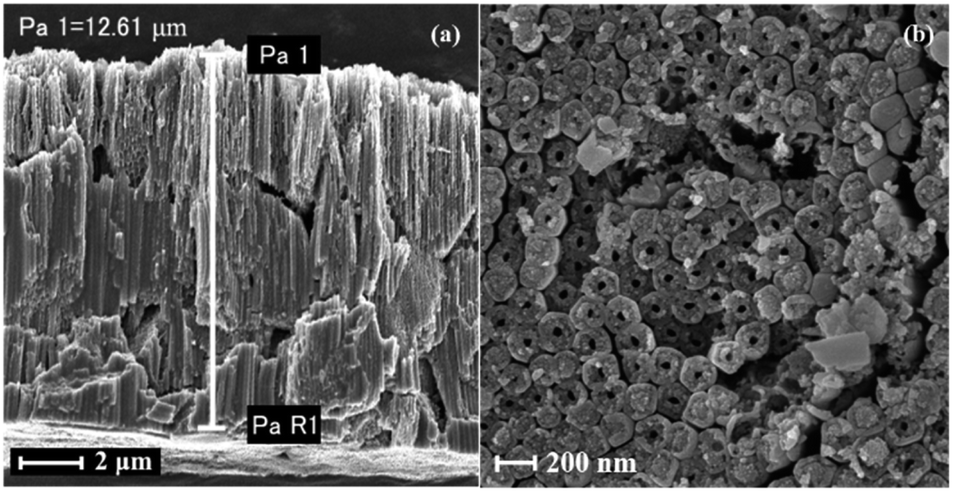 | ||
| Fig. 2 The (a) lateral and (b) bottom view SEM images of DW-ATNTAs. | ||
The specific surface area and pore parameters of the different photocatalysts are calculated according to the BET and BJH model, respectively, and are shown in Table 2. The specific surface area of DW-ATNTAs is 91.08 m2 g−1, which is higher than that of A-TiO2(plate) and SW-TNTAs. These results indicate that DW-ATNTAs can provide more adsorption sites and catalytic active sites for enhancing the photocatalytic performance of the nanotube arrays.
| Sample | SBET (m2 g−1) | VP (cm3 g−1) | DP (nm) |
|---|---|---|---|
| A-TiO2(plate) | 34.02 | 0.15 | 11.13 |
| SW-TNTAs | 57.69 | 0.34 | 21.10 |
| DW-ATNTAs | 91.08 | 0.26 | 16.07 |
The morphology of DW-ATNTAs is also clearly seen in the TEM image in Fig. 3. The tube wall images shows an alternately dark and bright pattern, indicating that it has a uniform double-walled shape. The size of the DW-ATNTAs are measured from the image in Fig. 3b. The diameters of outer and inner walls are 180 and 100 nm, respectively, which are consistent with the results of SEM. The element distributions of Ti, O, Al, and V in DW-ATNTAs are analyzed by high-resolution TEM element scanning in Fig. 3c, which shows that all the elements are evenly distributed across the tube wall. The relative brightness indicates that the element content of Ti is the highest, following by O, Al and V. The distribution of the elements in the inner and outer walls can be obtained by the STEM element line scanning (Fig. 3d). Taking the line scan map of the Ti element in DW-ATNTAs as an example, the element content of Ti in the inner wall is greater than that in the outer wall. This can be explained that the thicknesses of inner and outer walls are similar (about 20 nm), but the inner wall is a porous structure, causing the inner wall has a larger specific surface area. If the elements are evenly distributed in the two walls, the element content of the inner wall is more than that of the outer wall. The content of other elements is similar to Ti, which is a further indication that the alloy elements are uniformly distributed in the tubes.
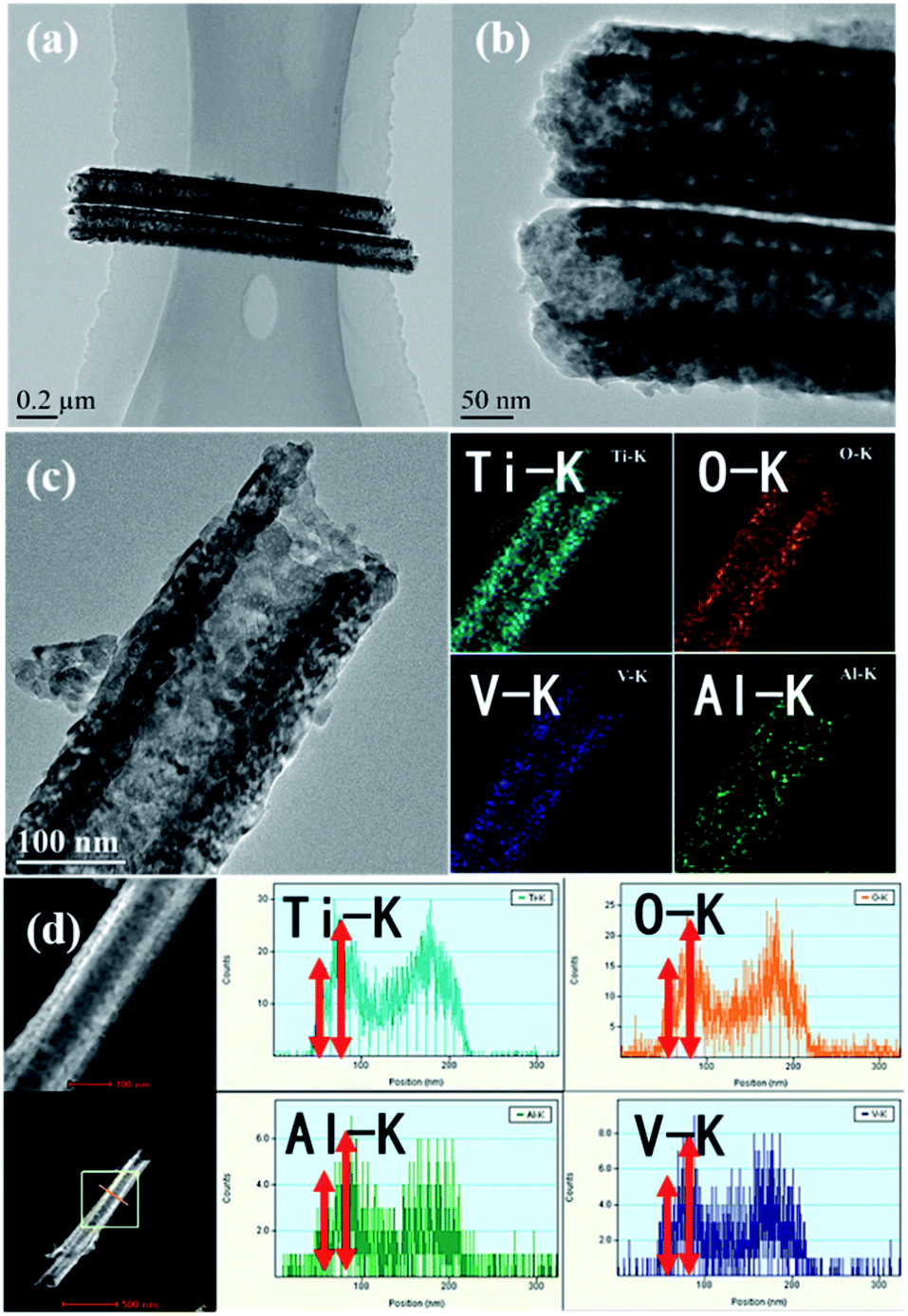 | ||
| Fig. 3 The (a) low-magnification and (b) high-magnification TEM images, (c) high resolution TEM element mapping and (d) STEM transverse spectral scans for different elements (Ti, O, Al, V) in DW-ATNTAs. | ||
The crystal phase structures of the photocatalysts are shown in Fig. 4. The diffraction peaks observed in all photocatalysts are at 25.4°, 37.8°, 48.0°, 54.0°, 55.1° and 62.8°, which correspond, respectively, to (101), (004), (200), (105), (211) and (204) reflections51–54 of anatase TiO2 (JCPDS no. 21-1272). There are no peaks characteristic of rutile TiO2 observed. X-ray photoelectron spectroscopy is used to explore the surface composition and the chemical state of the DW-ATNTAs (Fig. 5). The peaks of Ti, O, Al and V can be clearly identified in the full scan spectrum of DW-ATNTAs in Fig. 5a, which are corrected by referencing the C 1s peak at 284.60 eV. Fig. 5b is a high-resolution XPS of Ti 2p, combining the peaks at 464.2 and 458.5 eV of the 2p1/2 and 2p3/2 electrons in Ti 2p.55 The peak at 74.7 eV in Fig. 5c is attributed to Al 2p. The peaks at 524.95 and 517.45 eV in Fig. 5d are attributed to the 2p1/2 and 2p3/2 of V 2p,56 respectively. These XPS results indicates that the elements in the alloy exist in the form of the oxides TiO2, Al2O3 and V2O5.57
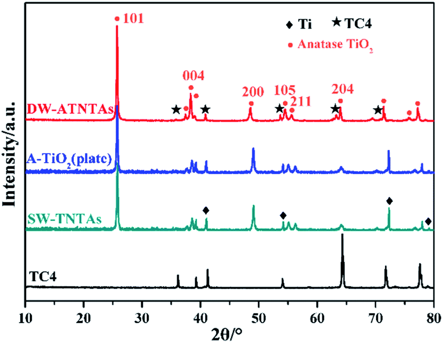 | ||
| Fig. 4 The XRD pattern of different morphology photocatalysts. | ||
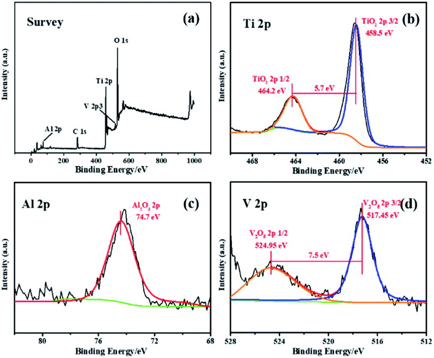 | ||
| Fig. 5 The (a) survey and high resolution (b) Ti 2p (c) Al 2p (d) V 2p XPS spectra of DW-ATNTAs. | ||
3.3 The formation mechanism of DW-ATNTAs
Previous study58 shows that during the anodization process, a C, F-rich oxide layer is formed on the wall surface of the nanotube arrays. The morphology of the wall changes as the C, F elements are removed during subsequent calcination. Therefore, the morphology, specific surface area and pore size distribution of DW-ATNTAs before and after calcination are examined in order to gain insight into the formation mechanism of double-walled nanotube arrays. The results of the analysis before calcination are shown in Fig. S6.† Comparing with the after calcination results show above in Fig. 1i–k, the nanotube arrays before calcination is classified as a single wall (Fig. S6a and b†), with the thickness is about 10 nm. Fig. S6c† shows the N2 adsorption/desorption isotherm and the pore size distribution of non-calcined DW-ATNTAs. The type II isotherm and H3 type hysteresis loop observed are attributed to a macroporous structure. After calcination (Fig. 1i and j), the DW-ATNTAs wall become thicker, as the double-walled and porous inner wall are formed, and the mesoporous distribution is concentrate around 20 nm while the macroporous distribution range more widely. Table S1† show the pore structure parameters of DW-ATNTAs before and after calcination. The specific surface area of DW-ATNTAs is 65.63 m2 g−1 before calcination, which increases to 91.08 m2 g−1 after calcination. The pore volume and pore diameter of the sample also increases correspondingly. These results show that the calcination process is the vital step to lead to the formation of the double-walled morphology and a mesoporous structure.To investigate the changes in element content on the surface of DW-ATNTAs during the process of synthesis, the elemental composition (Fig. S7†) is determined and present in Table 3. The chemical composition of the TC4 alloy surface before anodization (after electro-polishing) is 89.43 wt% Ti, 6.01 wt% Al, 2.64 wt% V and 1.92 wt% C. For the loss of V element, the contents of other elements are in accordance with the theoretical value. Table 3 shows that the content of Al element decrease more than 41.26% in the anodization process, while remaining essentially unchanged as a result of the calcination process. The content of V element shows little change as a result of either anodization or calcination. This means that V element is more stable in the alloy than Al in the synthesis process. Note that the C and F elements increase sharply as a result of anodization but reduce rapidly as a result of calcination, which suggests that the formation of the double-walled morphology is directly related to the change of C, F-rich oxide layer.
| Element/wt% | TC4 | Before anodizing | After anodizing | Δanodizing | After calcining | Δcalcining |
|---|---|---|---|---|---|---|
| Ti | 87–90 | 89.43 | 53.85 | −35.58 | 67.98 | 14.13 |
| Al | 5.5–6.8 | 6.01 | 3.53 | −2.48 | 3.75 | 0.22 |
| V | 3.5–4.5 | 2.64 | 2.43 | −0.21 | 2.40 | −0.03 |
| O | ≤0.2 | 0 | 22.15 | 22.15 | 23.31 | 1.16 |
| C | ≤0.1 | 1.92 | 10.91 | 8.99 | 2.56 | −8.35 |
| F | 0 | 0 | 7.13 | 7.13 | 0 | −7.13 |
To study the effect of V and Al element on the morphology during the synthesis process, alloy titanium dioxide nanotube arrays (ATNTAs) with three different V and Al compositions are compared. The top and lateral SEM images of the samples are shown in Fig. S8.† The results show that the nanotube array is easily corroded when the alloy contains only Ti and Al element. The addition of V element can improve the anti-corrosion property of the alloy significantly. However, when the element content of V in the alloy is increase beyond a certain point, the anti-corrosion property will be reduced. The XRD analysis (Fig. S9a†) shows that all of the ATNTAs are anatase phase. The UV-Vis DRS spectra (Fig. S9b†) shows that DW-ATNTAs has the narrowest forbidden band. The transient photocurrent curves of ATNTAs in Fig. S9c† shows that the DW-ATNTAs has the highest photocurrent. This observation shows that V element is the main factor affecting the visible light performance of the catalyst. XPS analyses (Fig. 5 and S10†) shows that the samples mainly contain Ti, O, Al and V elements, which exist independently in the form of the same oxides as TiO2, Al2O3, and V2O5 and no other oxide exist.
The changes of element composition on the surface of different ATNTAs during the process of synthesis is shown in Fig. S11 and summarized in Table S2.† The results show that the presence of Al element makes ATNTAs more susceptible to corrosion, while the addition of the proper amount of V element can enhance the anti-corrosion properties of alloy. However, as note above excessive addition of V element leads to more corrosion and the loss of Al and V. This conclusion is consistent with the SEM (Fig. S8†) results. The content of Al and V element show little changes during calcination, which indicates that the calcination process has little effect on the content of Al and V. A schematic diagram for the formation of the different ATNTAs is shown in Fig. S12.†
Based on these results, a proposed diagram for the formation of the double-walled porous nanotube arrays on TC4(6Al4V) is shown in Scheme 1. Due to the strong anti-corrosion property of pure TiO2, a C, F-rich oxide layer on the tube wall is too thin to form a double-walled nanotube array. However, during the anodization process, because the Al element makes TC4 more susceptible to be corroded, the dense alloy oxide layer of TC4 turns into nanoporous arrays under the corrosion by electrolyte firstly. Then, as the continuation of the anodization process, the wall of the nanoporous began to be separated, gradually forming independent nanotube arrays in the end. The inner wall surface of the nanotube arrays become a C, F-rich oxide layer after being in contact with electrolyte for a longer time than the outer wall during the anodization process. Later, during the calcination, this oxide layer transforms into a porous layer because the C and F elements are removed. Eventually, the special morphology of the double-walled with the porous inner wall is formed after calcination. Furthermore, the double-walled nanotube arrays structure will disappear and become nanoparticle arrays because of the overlong time in contact with the electrolyte (Fig. S3d and h†).
 | ||
| Scheme 1 The formation schematic of DW-ATNTAs. | ||
3.4 Photocatalytic activity of photocatalysts
A series of experiments are conducted to test the activity of the photocatalysts under visible light, and the results are shown in Fig. 6. Fig. 6a show the UV-Vis DRS of the photocatalysts with three different morphologies. The tangent intersects the X-axis at the inflection point of the line to obtain the maximum light response wavelength of photocatalysts, which are 402 nm for SW-TNTAs, 504 nm for A-TiO2(plate) and 607 nm for DW-ATNTAs. And the calculated forbidden band widths are: 3.08, 2.46, and 2.04 eV, respectively. The light absorption edge of the photocatalysts prepared by TC4 alloy is larger than 420 nm, which means that the material responds to visible light. The transient photocurrent curves of photocatalysts under visible light are shown in Fig. 6b. After 5 cycles of illumination and darkness, all photocatalysts maintain a high and stable current response. DW-ATNTAs has the largest current response of up to 0.75 × 10⁻⁵ A, which is about 3 times higher than that of SW-TNTAs. These results show that the DW-ATNTAs has excellent photoresponse performance. The performance of the photocatalysts are compared in the degradation of DBP in aqueous solution under visible light. The experimental results are shown in Fig. 6c. The blank test reveals that DBP is stable under visible light irradiation. After 3 h of irradiation, approximate 25% of DBP is simply adsorbed by SW-TNTAs and not degraded because of its wide band gap and insensitivities to visible light. About 50% of the DBP is degraded by A-TiO2(plate) because the range of light absorption extend. The DW-ATNTAs performs much better than either SW-TNTAs and A-TiO2(plate), with nearly 97% of DBP is degraded within 3 h. At the same time, DW-ATNTAs also shows an excellent adsorption performance for DBP. Taking the analysis of SEM and BET into consideration, the porous structure on the inner wall of DW-ATNTAs provides abundant adsorption sites and photocatalytic active sites for photocatalytic reaction, which greatly enhance the photocatalytic properties. As can be seen from Fig. 6d, the DBP degradation process follows pseudo first-order kinetics,20 i.e., ln(Ct/C0) = kt, where Ct is the concentration of DBP at a specific time t, C0 is the original concentration, and k is the degradation kinetic constant. In these experiments, the degradation kinetic constants of DBP under visible light of DW-ATNTAs, A-TiO2(plate) and SW-TNTAs are 14.42 × 10⁻³ min−1, 1.98 × 10⁻³ min−1 and 0.29 × 10⁻³ min−1, respectively. In short, the DW-ATNTAs exhibits excellent catalytic activity under visible light with a degradation kinetic constant is 7 and 50 times higher than that of A-TiO2(plate) and SW-TNTAs, respectively. That is higher than most of other reported TiO2 materials (Table S3†).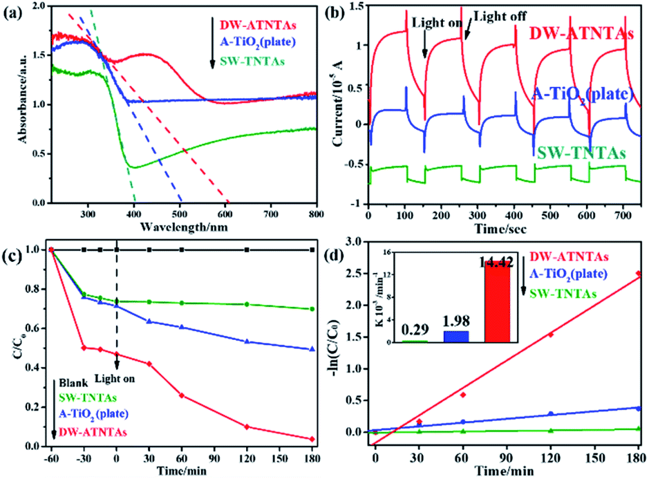 | ||
| Fig. 6 The (a) UV-Vis DRS, (b) i–t curve, (c) DBP removal efficiency and (d) kinetic equation curve with inset of kinetic constant of DBP removal of different morphology photocatalysts under visible light irradiation. | ||
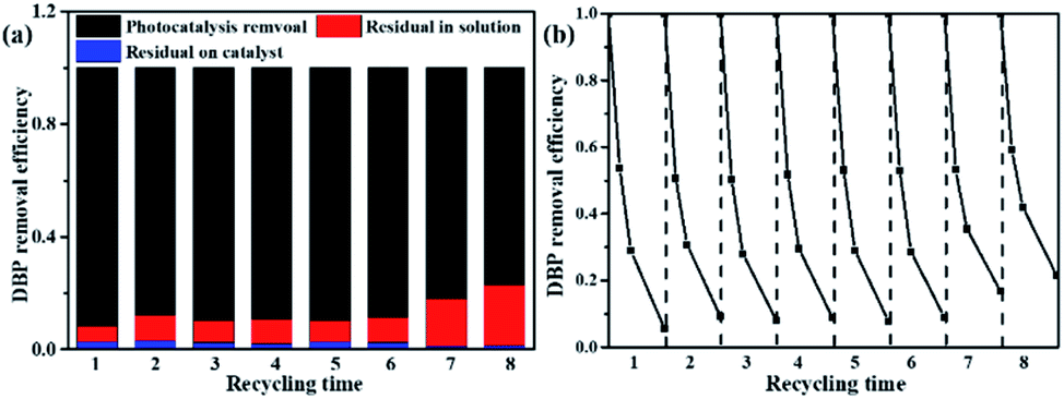
As shown in Fig. 7b, more than 91% of the photocatalytic activity of DW-ATNTAs is retained after 6 cycles, which indicates that DW-ATNTAs has a good photocatalytic recyclability. To investigate whether the DBP adsorbed on DW-ATNTAs is degraded, the DW-ATNTAs catalyst is immersed in methanol to desorb any residual DBP after the photocatalytic reaction. As shown in Fig. 7a, the amount of residual DBP on the catalyst after the reaction is very small. In short, the DBP is degraded repeatedly even though the efficiency drops slightly from one cycle to the next, showing that DW-ATNTAs is a stable catalyst.
 | ||
| Fig. 7 The (a) cyclic stability of DBP removal over DW-ATNTAs and (b) DBP desorption experiment with methanol after cyclic reaction under visible light irradiation. | ||
3.5 Photocatalytic active species of DBP degradation over DW-ATNTAs
To investigate the roles of the active species in the photocatalytic degradation of DBP, various scavengers, including ethylene diamine tetraacetic acid (EDTA) for h+, isopropyl alcohol (IPA) for ·OH and potassium bromate (KBrO3) for ·O2− are investigated.39 As shown in Fig. S13,† the photocatalytic degradation of DBP is almost entirely suppressed by EDTA addition and only slightly lower suppression occurred when IPA is used. These data indicate that the contribution of the active species in the photodecomposition is in the order of h+ > ·OH > ·O2−. The results also suggest that h+ can be in direct contact with the adsorbed DBP in the pores of DW-ATNTAs, so that h+ can be consumed in DBP degradation without being first converted to ·OH, thereby resulting in improvement for the photocatalytic efficiency of the reaction.Scheme 2 depicts these results of the photocatalytic degradation mechanism of DBP on the three different catalysts. The performance of A-TiO2(plate) is poor in both adsorption capacity and photocatalytic property for DBP degradation, because of the less of adsorption and catalytic sites on the flat plate. Then, the adsorption capacity of SW-TNTAs is enhanced, because of the morphology of nanotube arrays can provide a lot of adsorption sites, while the pure TiO2 nanotube arrays have a typically low response to visible light, resulting in the low photocatalytic degradation of DBP. Finally, the DW-ATNTAs utilize the V element in the TC4 alloy to in situ synthesize composite semiconductor nanotube arrays obviously improve the photoresponse to visible light. Its special morphology of double-walled and rich porous structure greatly increases the utilization rate of light and enhances the visible-light catalytic activity for DBP degradation.
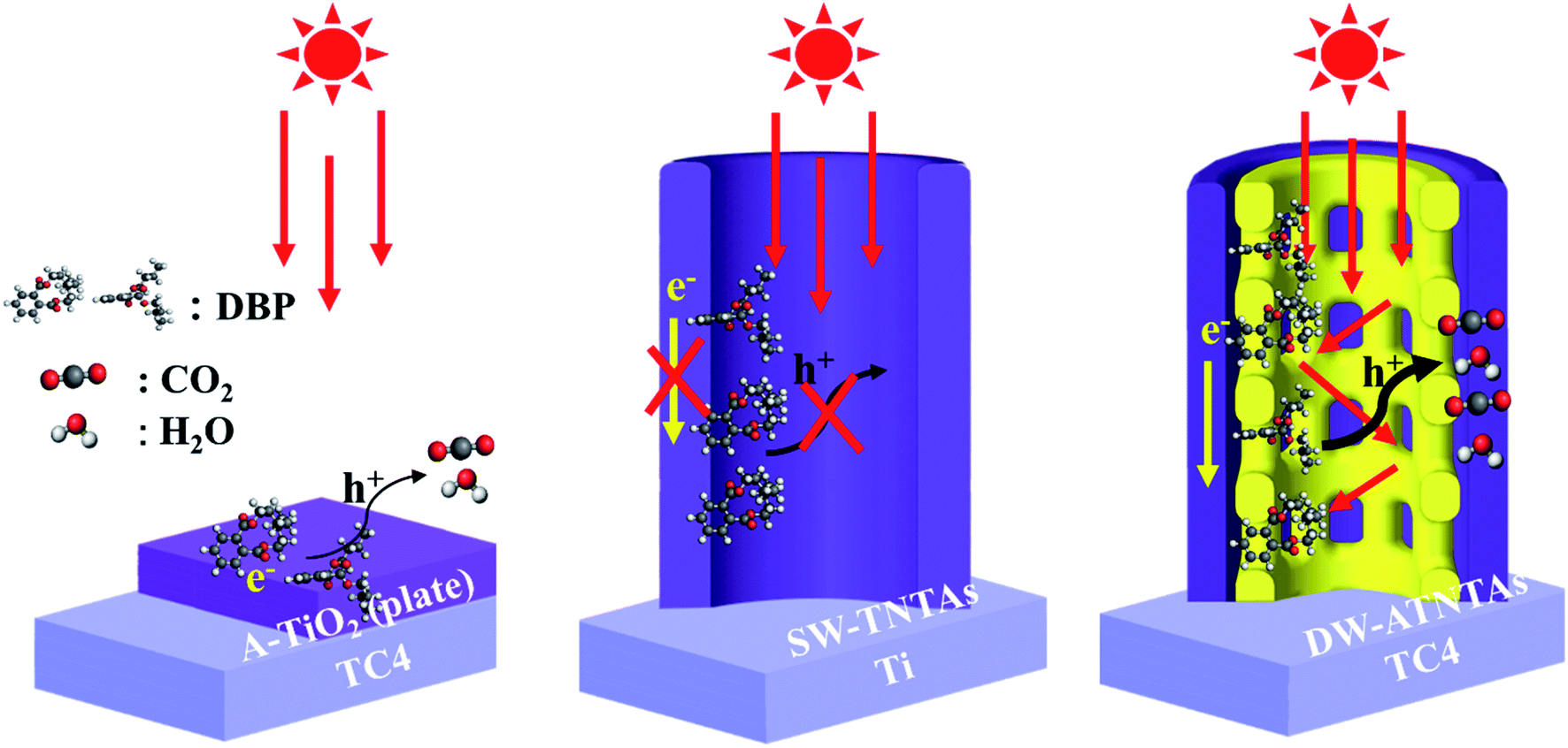 | ||
| Scheme 2 The schematic of DBP degradation over different morphologies photocatalysts under visible light irradiation. | ||
4. Conclusion
Double-walled alloy titanium dioxide nanotube arrays (DW-ATNTAs) with special porous inner walls and visible light response were fabricated by an in situ reaction through an improved anodization method. The V element of the alloy was oxidized which contributed to the visible light response of the DW-ATNTAs. At the same time, the inner wall porous structure of the DW-ATNTAs provided sufficient vacancy for adsorption and active sites for photocatalytic reaction, thereby greatly improving the photocatalytic activity of the materials. After visible light irradiation for 3 h, nearly 97% of DBP in an aqueous solution was removed with the degradation kinetic constant of DW-ATNTAs was 50 and 7 times higher than that of TNTAs and A-TiO2(plate), respectively. The special morphology of the double walls with the porous inner wall and smooth outer wall was attributed to the presence of V and Al and the formation of C, F-rich oxide layer. The anti-corrosion properties of the alloy caused by appropriate amount of V and Al. C, F-rich oxide layer was the fact that the inner wall was in contact with the electrolyte longer than the outer wall during the anodization process, which resulted in a thicker C, F-rich oxide layer on the surface of the inner wall. These led to an inner wall with a rich porous structure created through the removal of C, F elements during calcination at high temperature. This study provided a new avenue for the preparation of photocatalytic materials with special morphology and excellent visible light response.Conflicts of interest
There are no conflicts to declare.Acknowledgements
This work was supported by National Natural Science Foundation of China (21577039), Science and Technology Planning Project of Guangzhou City (201804020026). We are grateful to Dr Donald and Karen Barnes for providing helpful advice on our paper.Notes and references
- A. Fujishima and K. Honda, Nature, 1972, 238, 37 CrossRef CAS PubMed.
- G. A. Schurr and H. D. Wildt, US Pat. no. 4083946, 1978.
- S. You, Y. Hu and X. Liu, Appl. Catal., B, 2018, 232, 288 CrossRef CAS.
- H. Dong, X. Zhang and J. Li, Appl. Catal., B, 2020, 263, 118270 CrossRef.
- Z. Bai, Y. Hu and S. Yan, RSC Adv., 2017, 7, 1966 RSC.
- M. Ren, Y. Ao and P. Wang, Chem. Eng. J., 2019, 378, 122122 CrossRef CAS.
- F. Hayati, A. A. Isari and B. Anvaripour, Chem. Eng. J., 2020, 381, 123636 CrossRef.
- S. S. Rezaei, E. Dehghanifard and M. Noorisepehrb, J. Environ. Manage., 2019, 250, 109472 CrossRef CAS PubMed.
- M. Golshan, B. Kakavandi and M. Ahmadi, J. Hazard. Mater., 2018, 359, 325 CrossRef CAS PubMed.
- A. A. Isari, F. Hayati and B. Kakavandi, Chem. Eng. J., 2020, 392, 123685 CrossRef CAS.
- A. A. Isari, M. Mehregan and S. Mehregan, J. Hazard. Mater., 2020, 390, 122050 CrossRef CAS.
- B. Kakavandi, N. Bahari and R. R. Kalantary, Ultrason. Sonochem., 2019, 55, 75 CrossRef CAS PubMed.
- A. E. R. Mohamed and S. Rohani, Energy Environ. Sci., 2011, 4, 1065 RSC.
- M. Shaban, A. M. Ahmed and A. M. Rabie, J. Colloid Interface Sci., 2019, 555, 31 CrossRef CAS PubMed.
- L. Ji, X. Zhou and P. Schmuki, ChemElectroChem, 2019, 6, 114 CrossRef CAS.
- V. C. Anitha, A. N. Banerjee and S. W. Joo, Mater. Sci. Eng., B, 2015, 195, 1 CrossRef CAS.
- J. Chen, M. Jiang and W. Xu, Appl. Catal., B, 2019, 259, 118013 CrossRef CAS.
- X. Wang, X. Zhang and M. He, Res. Chem. Intermed., 2020, 46, 1663 CrossRef CAS.
- X. Yang, P. Ma and H. Qi, Nanoscale Res. Lett., 2017, 12, 1 CrossRef.
- G. He, J. Zhang and Y. Hu, Appl. Catal., B, 2019, 250, 301 CrossRef CAS.
- A. Kumar, M. Khan and X. Zeng, Chem. Eng. J., 2018, 353, 645 CrossRef CAS.
- W. A. Thompson, C. Perier and M. M. Maroto-Valer, Appl. Catal., B, 2018, 238, 136 CrossRef CAS.
- L. Cui, T. Pu and Z. Shen, Res. Chem. Intermed., 2019, 45, 2167 CrossRef CAS.
- S. Weon and W. Y. Choi, Environ. Sci. Technol., 2016, 50, 2556 CrossRef CAS PubMed.
- J. Wen, S. Sun and B. Zhang, RSC Adv., 2019, 9, 2693 Search PubMed.
- V. A. Tran, T. T. Truong and T. A. P. Phan, Appl. Surf. Sci., 2017, 399, 515 CrossRef CAS.
- L. Hou, S. Li and Y. Lin, J. Colloid Interface Sci., 2016, 466, 96 CrossRef.
- Y. Yang, S. Liao and W. Shi, RSC Adv., 2017, 18, 10885 RSC.
- L. Zhang, H. Cao and Y. Lu, J. Colloid Interface Sci., 2020, 568, 198 CrossRef CAS.
- K. Wu, P. Wu and J. Zhu, Chem. Eng. J., 2019, 360, 221 CrossRef CAS.
- A. R. Rafieerad, A. R. Bushroa and B. Nasiri-Tabrizi, RSC Adv., 2016, 13, 10527 RSC.
- L. Xia, Y. Xie and B. Fang, Chem. Eng. J., 2007, 9, 2397 Search PubMed.
- V. S. Saji, H. C. Choe and W. A. Brantley, Acta Biomater., 2009, 5, 2303 CrossRef CAS PubMed.
- D. Babilas, E. Urbańczyk and M. Sowa, Electrochim. Acta, 2016, 205, 256 CrossRef CAS.
- J. Song and A. Mukherjee, RSC Adv., 2016, 6, 82049 RSC.
- X. J. Feng, J. M. Macak and S. P. Albu, Acta Biomater., 2008, 4, 318 CrossRef CAS PubMed.
- A. Kazek-Kęsik, M. Krok-Borkowicz and G. Dercz, Electrochim. Acta, 2016, 204, 294 CrossRef.
- L. Peng, M. L. Eltgroth and T. J. LaTempa, Biomaterials, 2009, 30, 1268 CrossRef CAS PubMed.
- Z. Li, D. Ding and Q. Liu, Sensors, 2013, 13, 8393 CrossRef CAS PubMed.
- N. K. Allam, F. Alamgir and M. A. El-Sayed, ACS Nano, 2010, 4, 5819 CrossRef CAS.
- H. H. Nersisyan, B. U. Yoo and Y. M. Kim, Chem. Eng. J., 2016, 304, 232 CrossRef CAS.
- A. Devaraj, V. V. Joshi and A. Srivastava, Nat. Commun., 2016, 7, 11176 CrossRef CAS PubMed.
- X. Diao, Y. Hu and Y. He, RSC Adv., 2017, 7, 8338 RSC.
- K. Fushimi and H. Habazaki, Electrochim. Acta, 2009, 55, 258 CrossRef CAS.
- J. Naduvath, S. Mallick and T. Shripathi, Nanoscale, 2015, 7, 20386 RSC.
- S. Chen, Y. Chen and C. Li, Mater. Res. Express, 2018, 5, 4 Search PubMed.
- A. Kuvarega and B. Mamba, J. Nanomater., 2016, 9, 3746861 Search PubMed.
- M. Motola, H. Sopha and M. Krbal, Electrochem. Commun., 2018, 97, 1 CrossRef CAS.
- N. Wang, Z. Bai and Y. Qian, Adv. Mater., 2016, 28, 4126 CrossRef CAS PubMed.
- W. Chen, M. Yeh and L. Lin, ACS Sustain Chem Eng, 2018, 6, 3907 CrossRef CAS.
- M. M. Momeni, Y. Ghayeb and F. Ezati, J. Colloid Interface Sci., 2018, 514, 70 CrossRef CAS PubMed.
- X. Song, Y. Hu and M. Zheng, Appl. Catal., B, 2016, 182, 587 CrossRef CAS.
- J. Zhang, Y. Hu and J. Qin, Chem. Eng. J., 2020, 385, 123814 CrossRef.
- L. Yang, X. Wang and X. Mai, J. Colloid Interface Sci., 2019, 534, 459 CrossRef CAS PubMed.
- A. Zada, Y. Qu and S. Ali, J. Hazard. Mater., 2018, 342, 715 CrossRef CAS PubMed.
- S. Kundu, B. Satpati and T. Kar, J. Hazard. Mater., 2017, 339, 161 CrossRef CAS PubMed.
- X. Ning, W. Zhen and Y. Wu, Appl. Catal., B, 2018, 226, 373 CrossRef CAS.
- S. P. Albu, A. Ghicov and S. Aldabergenova, Adv. Mater., 2008, 20, 4135 CAS.
Footnote |
| † Electronic supplementary information (ESI) available: N2 adsorption/desorption isotherm, XRD, XPS, SEM, EDX, UV-Vis DRS, etc. See DOI: 10.1039/d0ra03627g |
| This journal is © The Royal Society of Chemistry 2020 |