
 Open Access Article
 This Open Access Article is licensed under a
 Creative Commons Attribution 3.0 Unported Licence
Position-locking of volatile reaction products by atmosphere and capping layers slows down photodecomposition of methylammonium lead triiodide perovskite†
Fengshuo Zu a,
Thorsten Schultzac,
Christian M. Wolffb,
Dongguen Shina,
Lennart Frohloffa,
Dieter Neherb,
Patrick Amsalema and
Norbert Koch*ac
a,
Thorsten Schultzac,
Christian M. Wolffb,
Dongguen Shina,
Lennart Frohloffa,
Dieter Neherb,
Patrick Amsalema and
Norbert Koch*ac
aInstitut für Physik & IRIS Adlershof, Humboldt-Universität zu Berlin, 12489 Berlin, Germany. E-mail: norbert.koch@physik.hu-berlin.de
bInstitut für Physik und Astronomie, Universität Potsdam, 14776 Potsdam, Germany
cHelmholtz-Zentrum Berlin für Materialien und Energie GmbH, 12489 Berlin, Germany
First published on 6th May 2020
Abstract
The remarkable progress of metal halide perovskites in photovoltaics has led to the power conversion efficiency approaching 26%. However, practical applications of perovskite-based solar cells are challenged by the stability issues, of which the most critical one is photo-induced degradation. Bare CH3NH3PbI3 perovskite films are known to decompose rapidly, with methylammonium and iodine as volatile species and residual solid PbI2 and metallic Pb, under vacuum under white light illumination, on the timescale of minutes. We find, in agreement with previous work, that the degradation is non-uniform and proceeds predominantly from the surface, and that illumination under N2 and ambient air (relative humidity 20%) does not induce substantial degradation even after several hours. Yet, in all cases the release of iodine from the perovskite surface is directly identified by X-ray photoelectron spectroscopy. This goes in hand with a loss of organic cations and the formation of metallic Pb. When CH3NH3PbI3 films are covered with a few nm thick organic capping layer, either charge selective or non-selective, the rapid photodecomposition process under ultrahigh vacuum is reduced by more than one order of magnitude, and becomes similar in timescale to that under N2 or air. We conclude that the light-induced decomposition reaction of CH3NH3PbI3, leading to volatile methylammonium and iodine, is largely reversible as long as these products are restrained from leaving the surface. This is readily achieved by ambient atmospheric pressure, as well as a thin organic capping layer even under ultrahigh vacuum. In addition to explaining the impact of gas pressure on the stability of this perovskite, our results indicate that covalently “locking” the position of perovskite components at the surface or an interface should enhance the overall photostability.
1 Introduction
Metal halide perovskites, owing to their remarkable optoelectronic characteristics1–4 have shown great potential not only in photovoltaic applications5–8 but also in light-emitting devices9,10 and photodetectors.11–13 In particular, perovskite solar cells have achieved tremendous accomplishments over the past decade, reaching a power conversion efficiency of over 25% for single junction cells.14 On the other hand, halide perovskite materials suffer from stability issues,15–25 of which the most critical one is that perovskites tend to degrade upon light exposure, thus impeding commercialization. Numerous studies have shown that the light-induced degradation process can be assisted by other factors, such as moisture,22,24 oxygen,22 an applied electric field,21 or simply vacuum.18,23 As pointed out by Tang et al.18 photo-induced degradation is found to be dependent on the environmental atmosphere, where the degradation upon illumination is significantly accelerated under vacuum. In addition, a recent study by Lin et al.26 found that an excess of charge carriers in the perovskite film upon photoexcitation can accelerate degradation, raising concerns about the materials' intrinsic stability. Nonetheless, it appears crucial to recognize the origin of instabilities of perovskites, especially in different environmental conditions and gas pressure. Therefore, further extensive investigations are needed towards a comprehensive understanding of the intrinsic degradation mechanisms of perovskite materials.In a previous study,23 we demonstrated that upon white light illumination the methylammonium lead mixed halide perovskites (MAPbIxCl3−x, MA: CH3NH3+) degrade rapidly under ultrahigh vacuum (UHV) conditions. Similar observations were also reported by Tang et al.,18 Juarez-Perez et al.,20 and Xu et al.25 who found that vacuum accelerates the photodecomposition process of perovskite films. However, the mechanism accountable for such a rapid photodecomposition process in vacuum has not been adequately explained yet. To provide an overall picture of the light-induced degradation mechanisms in different conditions of pressure and atmosphere, particularly the mechanism relating to the fast degradation process in vacuum, here we applied several complementary experimental techniques to study the optical, chemical, and electronic properties of the archetypical MAPbI3 perovskite, while exposing it to light in UHV, as well as under N2 and ambient air at atmospheric pressure. We demonstrate that upon white light illumination the rapid decomposition process of MAPbI3 into PbI2 and metallic Pb in UHV starts predominantly at the surface, resulting in significant changes in the structure and optoelectronic properties. In contrast, illumination in N2 and air does not induce substantial degradation even on the timescale of hours. In all cases, yet, we directly evidence the release of iodine from the perovskite surface as the cause for the instability of the perovskite upon photoexcitation. In addition, by employing charge selective and non-selective organic capping layers, the fast photodecomposition process in UHV can be tremendously reduced by restraining the volatile methylammonium and iodine from leaving the surface, indicating the effect of surrounding gas pressure being one of the key factors contributing to stability. Note that capping layers in ambient conditions were already shown to enhance perovskite stability, mainly by inhibiting the contact to water.27 While certainly great care must be taken when characterizing bare perovskite materials under (ultrahigh) vacuum conditions, our results also suggest that the back-reaction of volatile degradation products, when kept in proximity, to the parent perovskite is very efficient.
2 Results and discussion
2.1 Impact of environmental conditions on the photodecomposition process
To elucidate the effect of environmental conditions, with a focus on atmospheric pressure versus vacuum, on the photo-induced degradation process, MAPbI3 films prepared on poly(3,4-ethylenedioxythiophene):poly(styrenesulfonate) (PEDOT:PSS) substrates were exposed to white light (intensity equivalent to ca. 1.5 sun, with negligible UV spectral contribution below 400 nm) in UHV (base pressure of 5 × 10⁻⁹ mbar), as well as in atmospheric pressure of N2 and ambient air, respectively, while a variety of characterization techniques were applied to observe changes in the optical, chemical, morphological, and electronic properties. As displayed in Fig. 1a, upon illumination in UHV for 30 min we observe a drastic decrease of the optical absorption over the entire visible range, accompanied by an emergence of an absorption feature at ca. 2.5 eV. Such feature corresponds to the absorption of PbI2 and confirms the formation of PbI2, as also noted by other recent studies.18,20,25 In contrast to the case of UHV, illumination in N2 and in ambient air, even over extended time (up to 300 min), does not induce noticeable changes in the absorption spectra of Fig. 1a. To further investigate the effect of illumination on the chemical and structural properties, X-ray photoelectron spectroscopy (XPS) and X-ray diffraction (XRD) measurements were performed before and after different illumination treatments. As depicted in Fig. 1b, XRD patterns of all MAPbI3 films reveal a diffraction peak at 14.2°, which corresponds to the (110) reflection of the perovskite tetragonal structure [PDF 01-084-7607 (ICDD, 2018)]. The survey scan of the diffraction patterns can be found in Fig. S1 in the ESI.† Upon illumination in UHV one additional diffraction peak at 12.7° appears, which is assigned to the (001) reflection of the PbI2 hexagonal structure [PDF 00-007-0235 (ICDD, 1957)]. The appearance of a strong PbI2 diffraction peak indicates a severe photo-induced degradation in UHV condition, in agreement with the optical absorption results. In comparison, illumination in N2, even for a period of 300 min, does not induce noticeable formation of PbI2. We note that, however, illumination in ambient air produces a trace of PbI2, as shown in the magnified insets in Fig. 1b. Such a minor and rather slow photodecomposition process in ambient air is most likely assisted by the presence of water, as found in recent studies.18,22 | ||
Fig. 1 (a) UV-vis absorption spectra of a PbI2 film ( ), the pristine MAPbI3 perovskite films before ( ), the pristine MAPbI3 perovskite films before ( ), after illumination treatment in UHV for 30 min ( ), after illumination treatment in UHV for 30 min ( ), in N2 ( ), in N2 ( ), and ambient air ( ), and ambient air ( ) for 300 min, respectively. (b) X-ray diffraction patterns of a PbI2 film, and the MAPbI3 perovskite films before and after illumination in different environmental conditions. The magnified insets highlight the emergence of the PbI2 peak. Symbols Δ and * indicate the peak positions of PbI2 (001) and MAPbI3 (110), respectively. (c) Evolution of the stoichiometry (exclusive of the metallic Pb contributions) of the same set of perovskite films before and after illumination in different environmental conditions. The corresponding XPS spectra can be seen in Fig. S2–S4 of the ESI.† Above films were deposited on ITO/PEDOT:PSS substrates. ) for 300 min, respectively. (b) X-ray diffraction patterns of a PbI2 film, and the MAPbI3 perovskite films before and after illumination in different environmental conditions. The magnified insets highlight the emergence of the PbI2 peak. Symbols Δ and * indicate the peak positions of PbI2 (001) and MAPbI3 (110), respectively. (c) Evolution of the stoichiometry (exclusive of the metallic Pb contributions) of the same set of perovskite films before and after illumination in different environmental conditions. The corresponding XPS spectra can be seen in Fig. S2–S4 of the ESI.† Above films were deposited on ITO/PEDOT:PSS substrates. | ||
In addition to the structural changes, analysis of the evolution of the stoichiometry by XPS consistently reveals in an analogous manner that the composition of the MAPbI3 films has been largely modified upon light exposure in UHV, as illustrated in Fig. 1c. We observe severe loss of carbon and nitrogen, as well as a decrease of the relative iodine content by 40%, accompanied by the formation of a large amount of metallic Pb (Pb0) on the surface; further discussed in Fig. S2–S4.† Note that the seemingly increased iodine content in Fig. 1c is due to the fact that the sum of relative carbon, nitrogen, iodine, and lead components is 100% for each sample (only the metallic Pb amount is excluded in the atomic ratios), while the decrease of iodine content is estimated from the change in the absolute photoelectron intensity of iodine 3d5/2 peaks before and after illumination. In addition, angle-dependent XPS measurements, as presented in Fig. S5,† exhibit strongly varying Pb0/Pb2+ ratios (from 0.9 to 1.8) when changing the emission angle from 0° (normal emission) to 80°. Since XPS is a very surface sensitive method (probing depth of few nm) due to the short mean free path of photoelectrons,28 a change of the emission angle to off-normal enhances surface sensitivity even more. The variation of Pb0/Pb2+ ratios that we observe here thus indicates a vast enrichment of Pb0 at the surface, suggesting that the photodecomposition process proceeds from the surface on and does not occur homogeneously throughout the bulk. Consistent with the optical and structural changes induced by illumination in N2 and ambient air, we do not observe notable variations in the stoichiometry before and after illumination treatments, as seen in Fig. 1c. Furthermore, atomic force microscope (AFM) measurements, as displayed in Fig. S6,† show that the surface morphology is significantly modified after illumination in UHV, while the topographic features of the N2- and air-illuminated perovskite films remain very similar to those of the pristine samples. Specifically, the granular appearance of the film surfaces persists upon illumination, but the increase in surface roughness is much smaller in air and N2 (root-mean-square roughness increases from ca. 7 nm to ca. 9 nm) compared to UHV (roughness of ca. 38 nm), where also a few deep holes appear. Above observations confirm previous findings that photo-induced degradation is significantly accelerated in UHV and can be largely reduced in inert atmosphere, in agreement with the studies by Tang et al.18 and Juarez-Perez et al.20
To gain further insight into the photodecomposition process of the perovskite in the different environments, we further mounted an indium tin oxide (ITO)/glass coupon about 1 mm above the perovskite samples during light exposure, as illustrated in Fig. S7.† This ITO “cover” is used to “capture” volatile reaction products leaving the perovskite surface, to then be analyzed by XPS. Firstly, it is worth noting that in all environmental conditions we detected iodine on the ITO covers. This directly confirms the release of iodine from the perovskite films, as also found by Zhang et al.,29 Kim et al.,15 and Juarez-Perez et al.20 Furthermore, the release of iodine can accelerate the degradation process via chemical chain reactions, as suggested by Wang et al.16 In addition, we also noticed a slight increase of pressure during illumination in UHV, from 5 × 10⁻⁹ mbar to 3 × 10⁻⁸ mbar, which can be directly related to the release of iodine as well as CH3NH3+, as also concluded from the stoichiometry analysis above.
Furthermore, the impact of illumination on the electronic structure was examined by ultraviolet photoelectron spectroscopy (UPS), as displayed in Fig. 2. Here, all pristine perovskite films show nearly identical work function values of 4.94 ± 0.01 eV, as seen from the secondary electron cut-off (SECO) region, and exhibit highly reproducible valence band structures. As pointed out by Endres et al.30 and in our recent study,31 due to the very low density of states (DOS) from the highly dispersive top valence bands (VB), an accurate value of the VB onset can be achieved only on a logarithmic intensity scale, while values determined on a linear intensity scale overestimate the VB onset. Therefore, the valence band spectra are also presented on logarithmic scale, as shown in Fig. 2c, from which almost identical onset values of 0.80 ± 0.04 eV are observed for all pristine samples. After illumination in UHV, we observe that the valence band structure changes significantly, giving rise to noticeable DOS across the Fermi level (binding energy at 0 eV), as clearly seen in logarithmic scale in Fig. 2c. This DOS is ascribed to the high abundance of metallic Pb on the surface, as shown in Fig. S2,† which acts as donor-type surface states. Concomitantly, as seen from the SECO region, the work function decreased from 4.94 eV to 4.55 eV as a result of downward band bending induced by the Pb0-related donor-type surface states. In contrast and as expected, the UPS data for the illumination treated films in N2 and ambient air exhibit essentially the same SECO and VB spectral shape and energy position before and after light exposure. These UPS results suggest that, although the optical properties and electronic structure of the N2- and air-illuminated perovskite films remain mostly unchanged before and after light exposure, the degradation process has already commenced, as evidenced by the release of some iodine (from XPS measurements on the ITO covers). In short, we find that the photodecomposition process of MAPbI3 perovskite films highly depends on the environmental conditions, where fast degradation of MAPbI3 into solid PbI2 and metallic Pb and volatile methylammonium and iodine, in UHV condition occurs. This is in stark contrast to the situation in N2 and ambient air at atmospheric pressure, in which the photo-induced degradation is tremendously slowed down, in particular under the inert gas.
 | ||
| Fig. 2 UPS spectra of the same set of MAPbI3 perovskite films (from Fig. 1) before and after light exposure in UHV for 30 min, in N2 and ambient air for 300 min, respectively. Left panel (a) shows the SECO region, and middle (b) and right (c) panels show the valence band region on linear and logarithmic intensity scale, respectively. The dashed line in the right panel indicates the Fermi level at 0 eV binding energy. | ||
2.2 Impact of organic capping layers on the photodecomposition process
 | ||
Fig. 3 (a) UV-vis absorption spectra of a quartz/MAPbI3/PS film before ( ) and after light exposure ( ) and after light exposure ( ) in UHV for 60 min. (b) XRD patterns of the same set of samples before and after light exposure in UHV for 60 min, together with a pristine quartz/MAPbI3 film as a reference sample. Wide range XRD patterns are shown in Fig. S8a.† Symbols Δ and * indicate the peak position of PbI2 (001) and MAPbI3 (110), respectively. ) in UHV for 60 min. (b) XRD patterns of the same set of samples before and after light exposure in UHV for 60 min, together with a pristine quartz/MAPbI3 film as a reference sample. Wide range XRD patterns are shown in Fig. S8a.† Symbols Δ and * indicate the peak position of PbI2 (001) and MAPbI3 (110), respectively. | ||
Based on the above results, we thus propose the following photodecomposition reaction, where we explicitly consider the reaction rate for photo-induced degradation (rD) and that for the back-reaction to the parent perovskite (rB):

Upon photon (hν) absorption (which is part of above equation only for the degradation reaction, not for the back-reaction), volatile CH3NH3+ and I− ions are generated, and PbI2 may exist in an intermediate configuration. In vacuum, the volatile products are released from the surface, leaving behind (intermediate) PbI2. Subsequently, PbI2 can be decomposed into Pb0 and I2 via a photolysis reaction process.18 This photodegradation reaction can certainly take place also in the bulk, but since the reaction products remain in immediate vicinity the back-reaction can proceed with high rate, i.e., rD and rB are very similar, and photodegradation in the bulk is very slow overall. In contrast, the volatile degradation products can readily leave the surface in vacuum and rB approaches zero, resulting in continued decomposition and material loss. It is readily plausible that a solid capping layer, such as the PS layer in our experiments, reduces the loss rate of reaction products from the perovskite surface and thus enables the back-reaction rate rB to become large. Apparent from our experiments, the effect of the solid capping layer on the photodegradation kinetics is very similar to that of N2 and air at atmospheric pressure. The high collision rate of gas molecules (e.g., while at a pressure of 10−6 mbar it takes approx. 1 s that every surface site is hit by a gas atom, it takes only approx. 1 ns at atmospheric pressure) with the perovskite surface, and thus also the reaction products formed upon the photo-induced reaction, is sufficient to keep the volatile ions in close proximity on a time scale such that again rD ≈ rB. In turn, the macroscopically observed degradation process, yet ensuing from the solid surface onwards, is significantly slowed down compared to vacuum as environment.
 | ||
Fig. 4 UV-vis absorption spectra of (a) a quartz/MAPbI3/PCBM sample and (c) a PEDOT:PSS/MAPbI3/PCBM sample before ( ) and after ( ) and after ( ) light exposure in UHV for 60 min. (b) and (d) XRD patterns of the same set of samples from UV-vis absorption measurements. Symbol * indicates the (110) peak position of MAPbI3. ) light exposure in UHV for 60 min. (b) and (d) XRD patterns of the same set of samples from UV-vis absorption measurements. Symbol * indicates the (110) peak position of MAPbI3. | ||
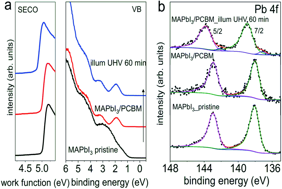
To further investigate this type of “electronically active” interface between MAPI3 and PCBM, we also fabricated a sample structure consisting of ITO/PEDOT:PSS/MAPbI3/PCBM, such that the density of the excess charge carriers is reduced in the perovskite layer upon photoexcitation, as a result of charge extraction and interface-mediated recombination at both interfaces.32,33 Analogous to the above results without hole extraction layer, we do not observe any change in the optical properties and structure before and after light exposure in UHV for 60 min, as seen from the absorption spectra in Fig. 4c and the XRD patterns in Fig. 4d.
However, these measurements are not sensitive to eventual minute changes at the very interface between MAPI3 and PCBM. Therefore, in addition, UPS and XPS measurements on the same set of samples with the configuration of ITO/PEDOT:PSS/MAPbI3/PCBM from Fig. 4, before and after light exposure in UHV were performed sequentially, and the corresponding spectra are shown in Fig. 5. Starting with a work function of 5.00 eV for the pristine perovskite film, essentially vacuum level alignment persists upon deposition of a thin PCBM layer (ca. 6 nm), as the complete heterostructure exhibits a work function of 4.98 eV. At this point we mention that a linear extrapolation on linear intensity scale of the photoemission onset is applied for the molecular semiconductors PCBM owing to its non-dispersive and Gaussian-shaped DOS.34 Therefore, the VB onset is found at 0.70 eV on a logarithmic intensity scale for the pristine perovskite film, and the onset of the top-layer PCBM highest occupied molecular orbital (HOMO) level at 1.30 eV on a linear intensity scale. The corresponding energy level diagrams are depicted in Fig. S9,† exhibiting a type II heterojunction. Consistent with initial interfacial vacuum level alignment, the Pb 4f peaks of MAPI3 remain at constant binding energy upon overcoating with PCBM. After visible light (ca. 1.5 sun) exposure in UHV for 60 min, however, we notice a very small amount of metallic Pb formed at the interface, as seen in the corresponding Pb 4f core level spectrum in Fig. 5b. This formation of Pb0 is accompanied by a release of elemental iodine, as evidenced by XPS measurements shown in Fig. S10,† which was obtained with the “ITO cover” technique described above. Apparently, the ca. 6 nm thin PCBM layer (deduced from the intensity attenuation of Pb 4f core levels) still enabled diffusion of the volatile iodine photo-induced degradation product and its loss through the sample surface. Such metallic Pb0, although at a very low density (Pb0/Pb2+ of 4.2%), is expected to act as donor-type surface state. Accordingly, we do observe a shift of the perovskite-related Pb 4f core level by 0.9 eV towards higher binding energy, as expected from the concomitant downward surface band bending in MAPI3 due to these surface states. As a side note, the presence of Pb0-related defects, mostly on the surface as depicted in Fig. S5,† could potentially enhance non-radiative interfacial recombination, which thereby degrades solar cell performance. Remarkably, the HOMO level of PCBM remains at the same binding energy after light exposure, which we attribute to the pinning of the lowest unoccupied molecular orbital (LUMO) level to the Pb0-related surface states, as schematically shown in the energy level diagram in Fig. S9b.† Consequently, the energy level alignment between the perovskite and the PCBM is markedly modified by illumination with visible light. Thus it is important to note that, while no obvious changes of chemical and structural properties from optical and XRD results were apparent, the electronic properties of the interface are much more sensitive to even minute compositional changes. If they go unnoticed, any correlation between assumed interfacial energy levels and device performance could be significantly flawed.
 | ||
| Fig. 5 Evolution of the UPS (a) and Pb 4f core levels spectra (b) of a pristine PEDOT:PSS/MAPbI3 sample upon deposition of a thin layer of PCBM, and subsequent light exposure in UHV for 60 min. | ||
We note that the sample temperature can rise up to 55 °C during the illumination in our experiments. As demonstrated by previous studies,23,35 a mild annealing up to 54 °C does not induce noticeable changes in the chemical and electronic structures of the perovskite films. However, the increased temperature during illumination can possibly accelerate the photodecomposition process, as pointed out by Misra et al.36
Finally, the above results substantiate that the rapid photodecomposition of MAPI3 in UHV can be significantly slowed down by depositing a solid organic capping layer onto the perovskite surface, because the degradation proceeds mainly from the surface onwards and not homogeneously throughout the bulk. The primary effect of the capping layer is to restrain the mobile CH3NH3+ and I− ions from escaping into vacuum, which, as a result, helps balancing the rates of the photo-induced decomposition reaction rD and the back-reaction to the parent perovskite rB. Notably, we conclude that surrounding gas at atmospheric pressure has the same effect in terms of improving the material's stability against photodegradation.
3 Conclusions
In summary, using complimentary experimental techniques we have shown that the photodecomposition process of MAPbI3 perovskite films is dominated by the loss of volatile reaction products (the methylammonium and iodine) from the surface, and that photo-induced degradation in the bulk plays a minor role. This loss is highly efficient in (ultrahigh) vacuum and leaves behind PbI2 and metallic Pb. The photo-induced degradation process can be significantly slowed down (much more than an order of magnitude) by exposing the perovskite surface to N2 or simply ambient air at atmospheric pressure, because the frequent collisions of gas atoms/molecules with the surface facilitate that the reaction products remain in close proximity for a prolonged time. This, in turn, enables the back-reaction to the parent perovskite to proceed with high effectiveness. A solid capping layer on top of the perovskite surface has a fully analogous effect. Notably, we do not find significant differences in the photo-induced decomposition kinetics for charge selective and non-selective capping layers. Yet, the back-reaction will not reach 100% and diffusion of reaction products through the capping layer will, over time, lead to complete loss of the perovskite. However, light-induced changes (due to perovskite photodegradation) in the electronic structure of interfaces between the perovskite and charge transport layers can occur way before significant decomposition could be noticed by common analytical methods. For the example of MAPI3 and PCBM, our photoemission results evidence that only 30 min illumination of the interface with 1.5 sun white light the interfacial energy level alignment is affected by up to 0.9 eV, a tremendous magnitude in terms of device function. At this stage, optical absorption and XRD measurements did not indicate any degradation yet, but we identified with photoemission experiments interfacial Pb0 formation and loss of iodine through the PCBM layer as causes. As noted by numerous others before, great care must be taken when characterizing perovskite materials using high dose photons, particularly in vacuum, as changes in the surface/interface electronic structure also impacts excited state and carrier spatial distribution and dynamics. Given that the surface is most critical for the stability of MAPI3, and probably also other perovskites, it should be worthwhile considering methods for covalent “locking” the surface components of the material in place.4 Experimental details
4.1 Sample preparation
The MAPbI3 perovskite films were prepared following our previous study,37 however, the 1![[thin space (1/6-em)]](https://www.rsc.org/images/entities/char_2009.gif) :1 molar ratio of methylammonium iodide to lead(II) iodide was changed to 1:0.95 in order to obtain a pure perovskite crystal structure without appearance of PbI2, as shown in Fig. S11 in the ESI.† Methylammonium iodide (MAI, 99%, anhydrous), lead(II) iodide (99.999% trace metals basis, beads), N,N-dimethylformamide (DMF) (99.8%, anhydrous) and diethyl ether (99.7%, anhydrous) were used as received from Sigma-Aldrich.
:1 molar ratio of methylammonium iodide to lead(II) iodide was changed to 1:0.95 in order to obtain a pure perovskite crystal structure without appearance of PbI2, as shown in Fig. S11 in the ESI.† Methylammonium iodide (MAI, 99%, anhydrous), lead(II) iodide (99.999% trace metals basis, beads), N,N-dimethylformamide (DMF) (99.8%, anhydrous) and diethyl ether (99.7%, anhydrous) were used as received from Sigma-Aldrich.
[6,6]-Phenyl C61 butyric acid methyl ester (PCBM, 99.9% from Sigma-Aldrich) films were fabricated by spin-coating the PCBM precursor (10 mg mL−1 in chlorobenzene) at 1000 rpm for 60 s onto the perovskite film. Polystyrene (PS) films were prepared by spin-coating the PS precursor (average molecular weight of 190.000, 10 mg mL−1 in 1,2-dichlorobenzene) at 1000 rpm for 60 s. Subsequently, the PCBM and PS films were annealed at 100 °C for 5 min. All films were prepared in the N2-filled glove box and transferred directly into the vacuum chamber under N2 atmosphere for photoemission measurements.
4.2 UV-vis absorption
UV-vis absorption measurements were performed in air using a Lambda 950 spectrometer (PerkinElmer) in transmission mode.4.3 X-ray diffraction
X-ray diffraction measurements were conducted in air using a Bruker D8 Advanced diffractometer at a wavelength of 0.154 nm.4.4 Photoemission spectroscopy
The X-ray and ultraviolet photoelectron spectroscopy (XPS and UPS) measurements shown in Fig. 1 and 2 were conducted at a JEOL JPS-9030 UHV system (base pressure of 1 × 10⁻⁹ mbar), using monochromatized Al Kα (1486.6 eV) radiation for XPS and hydrogen Lyman α (10.2 eV, Excitech)38 for UPS measurements. XPS and UPS experiments shown in Fig. 5 were performed at a SPECS UHV system (base pressure of 5 × 10⁻¹⁰ mbar), which is equipped with a monochromatized helium discharge lamp (21.22 eV) for UPS and a standard Mg Kα (1253.6 eV) X-ray source for XPS measurements. The SECO spectra were recorded at a bias of −10 V on the samples to overcome the work function of the analyzer. All spectra were recorded at room temperature and normal emission (unless otherwise stated).Sample illumination in different environmental conditions was conducted using a white halogen lamp (Solux MR16 4700 K, 50 watt, daylight rendering, the emission spectrum can be obtained at www.solux.net/cgi-bin/tlistore/infopages/4700k.html#TechnicalSpecifications) in UHV (base pressure of 5 × 10⁻⁹ mbar), in a N2-filled glove box (water and oxygen content less than 0.1 ppm), and in ambient air (relative humidity at 20%), respectively, at a controlled intensity of ca. 150 mW cm−2.
Author contributions
The project was conceived by F. Z. and N. K. F. Z. performed the characterizations, data analysis and wrote the first manuscript. F. S., D. S., C. W., and L. F. prepared the samples. All authors assisted with interpretation of the results and contributed to the writing of the manuscript.Conflicts of interest
There are no conflicts to declare.Acknowledgements
This work was supported by the Joint Graduate School HyPerCells of the University of Potsdam and the Helmholtz Zentrum Berlin, and the DFG (Project number 182087777-SFB951 and SPP2196).References
- S. De Wolf, J. Holovsky, S. J. Moon, P. Loper, B. Niesen, M. Ledinsky, F. J. Haug, J. H. Yum and C. Ballif, Organometallic Halide Perovskites: Sharp Optical Absorption Edge and Its Relation to Photovoltaic Performance, J. Phys. Chem. Lett., 2014, 5, 1035 CrossRef CAS PubMed.
- S. A. Kulkarni, T. Baikie, P. P. Boix, N. Yantara, N. Mathews and S. Mhaisalkar, Band-gap tuning of lead halide perovskites using a sequential deposition process, J. Mater. Chem. A, 2014, 2, 9221 RSC.
- A. Miyata, A. Mitioglu, P. Plochocka, O. Portugall, J. T.-W. Wang, S. D. Stranks, H. J. Snaith and R. J. Nicholas, Direct measurement of the exciton binding energy and effective masses for charge carriers in organic–inorganic tri-halide perovskites, Nat. Phys., 2015, 11, 582 Search PubMed.
- D. Shi, V. Adinolfi, R. Comin, M. Yuan, E. Alarousu, A. Buin, Y. Chen, S. Hoogland, A. Rothenberger, K. Katsiev, Y. Losovyj, X. Zhang, P. A. Dowben, O. F. Mohammed, E. H. Sargent and O. M. Bakr, Low trap-state density and long carrier diffusion in organolead trihalide perovskite single crystals, Science, 2015, 347, 519 CrossRef CAS PubMed.
- M. Stolterfoht, C. M. Wolff, Y. Amir, A. Paulke, L. Perdigón-Toro, P. Caprioglio and D. Neher, Approaching the fill factor Shockley–Queisser limit in stable, dopant-free triple cation perovskite solar cells, Energy Environ. Sci., 2017, 10, 1530 RSC.
- R. Wang, J. Xue, K.-L. Wang, Z.-K. Wang, Y. Luo, D. Fenning, G. Xu, S. Nuryyeva, T. Huang, Y. Zhao, J. L. Yang, J. Zhu, M. Wang, S. Tan, I. Yavuz, K. N. Houk and Y. Yang, Constructive molecular configurations for surface-defect passivation of perovskite photovoltaics, Science, 2019, 366, 1509 CrossRef CAS PubMed.
- W. S. Yang, J. H. Noh, N. J. Jeon, Y. C. Kim, S. Ryu, J. Seo and S. I. Seok, High-performance photovoltaic perovskite layers fabricated through intramolecular exchange, Science, 2015, 348, 1234 CrossRef CAS PubMed.
- H. Zhou, Q. Chen, G. Li, S. Luo, T.-b. Song, H.-S. Duan, Z. Hong, J. You, Y. Liu and Y. Yang, Interface engineering of highly efficient perovskite solar cells, Science, 2014, 345, 542 CrossRef CAS PubMed.
- N. Wang, L. Cheng, R. Ge, S. Zhang, Y. Miao, W. Zou, C. Yi, Y. Sun, Y. Cao, R. Yang, Y. Wei, Q. Guo, Y. Ke, M. Yu, Y. Jin, Y. Liu, Q. Ding, D. Di, L. Yang, G. Xing, H. Tian, C. Jin, F. Gao, R. H. Friend, J. Wang and W. Huang, Perovskite light-emitting diodes based on solution-processed self-organized multiple quantum wells, Nat. Photon., 2016, 10, 699 CrossRef CAS.
- M. A. Becker, R. Vaxenburg, G. Nedelcu, P. C. Sercel, A. Shabaev, M. J. Mehl, J. G. Michopoulos, S. G. Lambrakos, N. Bernstein, J. L. Lyons, T. Stöferle, R. F. Mahrt, M. V. Kovalenko, D. J. Norris, G. Rainò and A. L. Efros, Bright triplet excitons in caesium lead halide perovskites, Nature, 2018, 553, 189 CrossRef CAS PubMed.
- M. Zhang, F. Zhang, Y. Wang, L. Zhu, Y. Hu, Z. Lou, Y. Hou and F. Teng, High-Performance Photodiode-Type Photodetectors Based on Polycrystalline Formamidinium Lead Iodide Perovskite Thin Films, Sci. Rep., 2018, 8, 11157 CrossRef PubMed.
- H. Wang and D. H. Kim, Perovskite-based photodetectors: materials and devices, Chem. Soc. Rev., 2017, 46, 5204 RSC.
- J. Ding, S. Du, Y. Zhao, X. Zhang, Z. Zuo, H. Cui, X. Zhan, Y. Gu and H. Sun, High-quality inorganic–organic perovskite CH3NH3PbI3 single crystals for photo-detector applications, J. Mater. Sci., 2016, 52, 276 CrossRef.
- https://www.nrel.gov/pv/assets/pdfs/cell_efficiency_explanatory_notes.pdf.
- G. Y. Kim, A. Senocrate, T.-Y. Yang, G. Gregori, M. Grätzel and J. Maier, Large tunable photoeffect on ion conduction in halide perovskites and implications for photodecomposition, Nat. Mater., 2018, 17, 445 CrossRef CAS PubMed.
- S. Wang, Y. Jiang, E. J. Juarez-Perez, L. K. Ono and Y. Qi, Accelerated degradation of methylammonium lead iodide perovskites induced by exposure to iodine vapour, Nat. Energy, 2016, 2, 16195 CrossRef.
- N. Aristidou, C. Eames, I. Sanchez-Molina, X. Bu, J. Kosco, M. S. Islam and S. A. Haque, Fast oxygen diffusion and iodide defects mediate oxygen-induced degradation of perovskite solar cells, Nat. Commun., 2017, 8, 15218 CrossRef PubMed.
- X. Tang, M. Brandl, B. May, I. Levchuk, Y. Hou, M. Richter, H. Chen, S. Chen, S. Kahmann, A. Osvet, F. Maier, H.-P. Steinrück, R. Hock, G. J. Matt and C. J. Brabec, Photoinduced degradation of methylammonium lead triiodide perovskite semiconductors, J. Mater. Chem. A, 2016, 4, 15896 RSC.
- N. N. Shlenskaya, N. A. Belich, M. Grätzel, E. A. Goodilin and A. B. Tarasov, Light-induced reactivity of gold and hybrid perovskite as a new possible degradation mechanism in perovskite solar cells, J. Mater. Chem. A, 2018, 6, 1780 RSC.
- E. J. Juarez-Perez, L. K. Ono, M. Maeda, Y. Jiang, Z. Hawash and Y. Qi, Photodecomposition and thermal decomposition in methylammonium halide lead perovskites and inferred design principles to increase photovoltaic device stability, J. Mater. Chem. A, 2018, 6, 9604 RSC.
- S. Bae, S. Kim, S. W. Lee, K. J. Cho, S. Park, S. Lee, Y. Kang, H. S. Lee and D. Kim, Electric-Field-Induced Degradation of Methylammonium Lead Iodide Perovskite Solar Cells, J. Phys. Chem. Lett., 2016, 7, 3091 CrossRef CAS PubMed.
- N. H. Nickel, F. Lang, V. V. Brus, O. Shargaieva and J. Rappich, Unraveling the Light-Induced Degradation Mechanisms of CH3NH3PbI3 Perovskite Films, Adv. Electron. Mater., 2017, 3, 1700158 CrossRef.
- F.-S. Zu, P. Amsalem, I. Salzmann, R.-B. Wang, M. Ralaiarisoa, S. Kowarik, S. Duhm and N. Koch, Impact of White Light Illumination on the Electronic and Chemical Structures of Mixed Halide and Single Crystal Perovskites, Adv. Opt. Mater., 2017, 5, 1700139 CrossRef.
- J. F. Galisteo-Lopez, M. Anaya, M. E. Calvo and H. Miguez, Environmental Effects on the Photophysics of Organic–Inorganic Halide Perovskites, J. Phys. Chem. Lett., 2015, 6, 2200 CrossRef CAS PubMed.
- R. P. Xu, Y. Q. Li, T. Y. Jin, Y. Q. Liu, Q. Y. Bao, C. O'Carroll and J. X. Tang, In Situ Observation of Light Illumination-Induced Degradation in Organometal Mixed-Halide Perovskite Films, ACS Appl. Mater. Interfaces, 2018, 10, 6737 CrossRef CAS PubMed.
- Y. Lin, B. Chen, Y. Fang, J. Zhao, C. Bao, Z. Yu, Y. Deng, P. N. Rudd, Y. Yan, Y. Yuan and J. Huang, Excess charge-carrier induced instability of hybrid perovskites, Nat. Commun., 2018, 9, 4981 CrossRef PubMed.
- K. O. Brinkmann, J. Zhao, N. Pourdavoud, T. Becker, T. Hu, S. Olthof, K. Meerholz, L. Hoffmann, T. Gahlmann, R. Heiderhoff, M. F. Oszajca, N. A. Luechinger, D. Rogalla, Y. Chen, B. Cheng and T. Riedl, Suppressed decomposition of organometal halide perovskites by impermeable electron-extraction layers in inverted solar cells, Nat. Commun., 2017, 8, 13938 CrossRef CAS PubMed.
- M. P. Seah and W. A. Dench, Quantitative electron spectroscopy of surfaces: A standard data base for electron inelastic mean free paths in solids, Surf. Interface Anal., 1979, 1, 2 CrossRef CAS.
- F. Zhang, F. Ullrich, S. Silver, R. A. Kerner, B. P. Rand and A. Kahn, Complexities of Contact Potential Difference Measurements on Metal Halide Perovskite Surfaces, J. Phys. Chem. Lett., 2019, 890 CrossRef CAS PubMed.
- J. Endres, D. A. Egger, M. Kulbak, R. A. Kerner, L. Zhao, S. H. Silver, G. Hodes, B. P. Rand, D. Cahen, L. Kronik and A. Kahn, Valence and Conduction Band Densities of States of Metal Halide Perovskites: A Combined Experimental–Theoretical Study, J. Phys. Chem. Lett., 2016, 7, 2722 CrossRef CAS PubMed.
- F. Zu, P. Amsalem, D. A. Egger, R. Wang, C. M. Wolff, H. Fang, M. A. Loi, D. Neher, L. Kronik, S. Duhm and N. Koch, Constructing the Electronic Structure of CH3NH3PbI3 and CH3NH3PbBr3 Perovskite Thin Films from Single-Crystal Band Structure Measurements, J. Phys. Chem. Lett., 2019, 10, 601 CrossRef PubMed.
- P. Caprioglio, M. Stolterfoht, C. M. Wolff, T. Unold, B. Rech, S. Albrecht and D. Neher, On the Relation between the Open-Circuit Voltage and Quasi-Fermi Level Splitting in Efficient Perovskite Solar Cells, Adv. Energy Mater., 2019, 9, 1901631 CrossRef.
- C. M. Wolff, F. Zu, A. Paulke, L. P. Toro, N. Koch and D. Neher, Reduced Interface-Mediated Recombination for High Open-Circuit Voltages in CH3NH3PbI3 Solar Cells, Adv. Mater., 2017, 1700159 CrossRef PubMed.
- M. Oehzelt, N. Koch and G. Heimel, Organic semiconductor density of states controls the energy level alignment at electrode interfaces, Nat. Commun., 2014, 5, 4174 CrossRef CAS PubMed.
- M. Ralaiarisoa, I. Salzmann, F.-S. Zu and N. Koch, Effect of Water, Oxygen, and Air Exposure on CH3NH3PbI3–xClx Perovskite Surface Electronic Properties, Adv. Electron. Mater., 2018, 1800307 CrossRef.
- R. K. Misra, S. Aharon, B. Li, D. Mogilyansky, I. Visoly-Fisher, L. Etgar and E. A. Katz, Temperature- and Component-Dependent Degradation of Perovskite Photovoltaic Materials under Concentrated Sunlight, J. Phys. Chem. Lett., 2015, 6, 326 CrossRef CAS PubMed.
- D. Shin, D. Kang, J.-B. Lee, J.-H. Ahn, I.-W. Cho, M.-Y. Ryu, S. W. Cho, N. E. Jung, H. Lee and Y. Yi, Electronic Structure of Nonionic Surfactant-Modified PEDOT:PSS and Its Application in Perovskite Solar Cells with Reduced Interface Recombination, ACS Appl. Mater. Interfaces, 2019, 11, 17028 CrossRef CAS PubMed.
- A. M. Boehm, J. Wieser, K. Butrouna and K. R. Graham, A new photon source for ultraviolet photoelectron spectroscopy of organic and other damage-prone materials, Org. Electron., 2017, 41, 9 CrossRef CAS.
Footnote |
| † Electronic supplementary information (ESI) available. See DOI: 10.1039/d0ra03572f |
| This journal is © The Royal Society of Chemistry 2020 |