
 Open Access Article
 This Open Access Article is licensed under a Creative Commons Attribution-Non Commercial 3.0 Unported Licence
Impact of N-substitution on structural, electronic, optical, and vibrational properties of a thiophene–phenylene co-oligomer†
Vasiliy A. Trukhanov *ab,
Dmitry I. Dominskiya,
Olga D. Parashchuka,
Elizaveta V. Feldmana,
Nikolay M. Surinc,
Evgeniya A. Svidchenkoc,
Maxim S. Skorotetckyc,
Oleg V. Borshchevc,
Dmitry Yu. Paraschuka and
Andrey Yu. Sosorevab
*ab,
Dmitry I. Dominskiya,
Olga D. Parashchuka,
Elizaveta V. Feldmana,
Nikolay M. Surinc,
Evgeniya A. Svidchenkoc,
Maxim S. Skorotetckyc,
Oleg V. Borshchevc,
Dmitry Yu. Paraschuka and
Andrey Yu. Sosorevab
aFaculty of Physics & International Laser Centre of Lomonosov Moscow State University, Leninskiye Gory 1/62, Moscow 119991, Russia. E-mail: trukhanov@physics.msu.ru
bInstitute of Spectroscopy of the Russian Academy of Sciences, Fizicheskaya St. 5, Troitsk, Moscow 108840, Russia
cEnikolopov Institute of Synthetic Polymeric Materials of Russian Academy of Sciences, Profsoyuznaya St. 70, Moscow 117393, Russia
First published on 27th July 2020
Abstract
Properties of the organic semiconductors can be finely tuned via changes in their molecular structure. However, the relationship between the molecular structure, molecular packing, and (opto)electronic properties of the organic semiconductors to guide their smart design remains elusive. In this study, we address computationally and experimentally the impact of subtle modification of a thiophene–phenylene co-oligomer CF3-PTTP-CF3 on the molecular properties, crystal structure, charge transport, and optoelectronic properties. This modification consists in the substitution of two C–H atom pairs by N atoms in the thiophene units and hence converting them to thiazole units. A dramatic effect of the N-substitution on the crystal structure—the crossover from the herringbone packing motif to π-stacking—is attributed to significant changes in the molecular electrostatic potential. The changes in the molecular and crystal structure resulting from the N-substitution clearly reveal themselves in the Raman spectra. The increase of the calculated electron mobility in the corresponding crystals as a result of the N-substitution is rationalized in terms of the changes in the molecular and crystal structure. The charge transport, electroluminescence, and photoelectric properties are compared in thin-film organic field-effect transistors based on CF3-PTTP-CF3 and its N-substituted counterpart. An intriguing similarity between the effects of N-substitution in the thiophene rings and fluorination of the thiophene–phenylene oligomer is revealed, which is probably associated with a more general effect of electronegative substitution. The obtained results are anticipated to facilitate the rational design of organic semiconductors.
1. Introduction
Organic semiconductors (OSs) with high charge-carrier mobility and efficient luminescence are necessary for organic optoelectronic devices, e.g., organic light-emitting diodes,1 organic light-emitting transistors,2 and electrically pumped solid-state organic lasers.3 These features are luckily combined in conjugated oligomers and co-oligomers, which makes these compounds promising candidates for using in organic optoelectronics.4 Some (co)oligomers combine strong light absorption in UV-vis spectral region with decent charge-carrier mobility so that the photoelectric effect can be efficient making them useful for development of novel organic phototransistors.5 Moreover, synthetic flexibility of the conjugated (co)oligomers enables their prompt chemical modification for fine-tuning of the electronic and optical properties.Although a plenty of conjugated (co-)oligomers were synthesized, the structure–property relationships for their rational design remain poorly understood. Specifically, it is well known that very small changes in the chemical structure can dramatically affect the crystal packing and physico-chemical properties of the OSs (see, e.g., ref. 6–9). For instance, substitution of hydrogen atoms with fluorine ones (fluorination) typically facilitates a crossover from the herringbone packing commonly observed in OS crystals to the π-stacking motif, which is considered more favorable for charge transport.7–15 However, the effect of fluorination on the optoelectronic properties is not always positive: in several cases, fluorination results in a decrease in photoluminescence quantum yield (PLQY) and absorption,9 and extensive fluorination can deteriorate the charge mobility.7,8,16 Moreover, in exotic cases fluorination induces the opposite crossover in the crystal structure—from the π-stacking to herringbone motif.17–19 Thus, it is important to predict whether certain changes in the molecular (chemical) structure will be favorable or detrimental for optoelectronic applications. This prediction could be based on general “molecular structure – crystal structure – (opto)electronic properties” relationships, which are now in the focus of the material science.
Very recently, two ways of tailoring the optoelectronic properties of the thiophene–phenylene co-oligomers—addition of terminal groups20 and fluorination16—have been investigated in detail. However, there is another tool for tuning the OS properties—the heteroatomic substitution in the very conjugated core. This type of modification can have a stronger impact on the optoelectronic properties because it is directly related to the distribution of the electron density at the frontier molecular orbitals, which determine the optoelectronic properties. Among heteroatoms, nitrogen attracts a particular attention. Introduction of nitrogen into the conjugated core of the OSs (intra-ring N-substitution) significantly decreases the energies of the frontier orbitals and can change the conductivity type from the hole to electron one.21,22 An interesting material among the N-substituted conjugated co-oligomers is 2,2′bis[4-(trifluoromethyl)phenyl]-5,5′-bi-1,3-thiazole (CF3-PTzTzP-CF3) (see Fig. 1 for chemical structure). According to ref. 23 and 24, the electron mobility, μe, in CF3-PTzTzP-CF3 exceeds that in CF3-PTTP-CF3 (its counterpart without nitrogen) by an order of magnitude. The μe value higher than 1 cm2 V−1 s−1 reported in ref. 23 for CF3-PTzTzP-CF3 is very unusual for oligomers and is usually observed for fused aromatics,25 which generally show more favorable molecular packing with the stronger electronic interaction between the molecules. The earlier computational studies reproduced the reported difference in μe in the two aforementioned oligomers.26,27 The difference was tentatively assigned to the dramatic difference in the crystal structure for the two compounds: while CF3-PTTP-CF3 packs in a herringbone motif typical for OSs, CF3-PTzTzP-CF3 shows π-stacking, which is considered beneficial for charge transport.28,29 But what is the mechanism underlying the change of the crystal packing for these compounds? Is this mechanism specific for these compounds or general for conjugated oligomers? And does the N-substitution affect optical properties of conjugated (co)oligomers? These questions have not been answered yet.
 | ||
| Fig. 1 Chemical structure of the compounds studied. | ||
In this study, we address computationally and experimentally the structure–property relationships underlying the difference in the properties between CF3-PTTP-CF3 and CF3-PTzTzP-CF3. Specifically, we focus on the relationships between the molecular structure and properties, the molecular and crystal structures, and impact of the molecular/crystal structure on the charge-carrier mobility. First, density functional theory (DFT) calculations along with absorption, photoluminescence (PL) and Raman spectroscopies are applied to compare the electronic, optical, and vibrational properties of the isolated molecules. Then, the physics underlying the difference in the crystal packing is unraveled, and the impact of this difference on charge mobility is modeled. To explore the potential of both oligomers for (opto)electronic devices, organic field-effect transistors (OFETs) with thin-film active layers of both oligomers are fabricated and studied, and they demonstrate electroluminescence and a photoelectric effect. The observed impact of the intra-ring N-substitution on the structural, electronic, vibrational, optical and charge-transport properties is compared with the effect of fluorination recently addressed in ref. 16, and intriguing similarities possibly related to general relationships between the molecular structure, crystal structure and (opto)electronic properties are revealed.
2. Methods
2.1. Calculations
Density functional theory (DFT) and time-dependent DFT (TDDFT) calculations were performed using GAMESS package30,31 at B3LYP/6-31G(d,p) level. The reorganization energy for electron transport, λ, was approximated by its inner-sphere part, which is typically considered much larger than the outer-sphere part for OSs.32 The λ values were calculated according to the common adiabatic potentials (4-point) scheme33 from the energies of the molecule in the following four states: the neutral state in its optimized geometry (EN), the neutral state in the optimized geometry of the negatively charged state (EN*), the negatively charged state in its optimized geometry (EC), and the negatively charged state in the geometry of the neutral state (EC*): λ = (EN* − EN) + (EC* − EC). Electron transfer integrals Ji were calculated using a home-written code based on the dimer projection method (DIPRO).34–36 Electrostatic potential was visualized using JMol package,37 and molecular orbitals were visualized using Chemcraft.38 Conjugated lengths were calculated as suggested in ref. 16. Hirshfeld surface analysis and energy framework calculations were performed at B3LYP/6-31g(d,p) level in CrystalExplorer17.5 software.39,402.2. Sample preparation
The CF3-PTTP-CF3 was synthesized according to previous work41 and CF3-PTzTzP-CF3 (97% purity) was purchased in Sigma-Aldrich.2.3. Raman spectroscopy
For Raman measurements, powders of CF3-PTTP-CF3 and CF3-PTzTzP-CF3 were compressed into tablets. Raman measurements in the spectral range 10–1800 cm−1 were conducted using a Raman microscope (inVia, Renishaw) with a 50× objective lens (Leica DM 2500 M, NA = 0.75). The excitation wavelength was 633 nm provided by a He–Ne laser (RL633, Renishaw) with the maximum power of 17 mW. Low-frequency (LF) measurements were conducted using a NExT monochromator, high-frequency (HF) measurements were performed with a 633 nm edge filter. The LF and HF measurements were performed separately, and then the LF and HF spectra were merged. The accumulation time and the pump intensity were selected to increase the signal-to-noise ratio and minimize photodegradation. All spectra were measured in several points of the sample and then averaged to reduce the anisotropy effect on the Raman spectra.2.4. Absorption and photoluminescence
The absorption spectra were recorded on a Shimadzu UV-2501PC spectrophotometer in a 10 mm-thick photometric quartz cuvette using tetrahydrofuran (THF) solutions with the oligomer concentrations of 10−5 M. Photoluminescence spectra (PL) in solution were recorded by using of a scanning spectrofluorimeter ALS01M operating in the single-photon-counting mode.42 The PL measurements were carried out in the 90°-geometry for several optical densities of the sample in the range of 0.06–0.12 absorbance units by using a 10 mm-thick cuvette. The PL quantum yield (QY) was measured by comparing the integral PL intensity of 10−6 M diluted solutions in THF with the integral PL intensity of the standard as described elsewhere.43 As a PLQY standard, solution of 1,4-bis(5-phenyloxazol-2-yl)benzene (POPOP) in cyclohexane (PLQY = 0.93) was used.2.5. OFET fabrication and characterization
OFET samples were fabricated in the top-contact bottom-gate architecture on silicon substrates with 200 nm-thick thermally grown oxide (SiO2) dielectric layer covered with a poly(methylmethacrylate) (PMMA) or hexamethyldisilazane (HMDS) layer. Si/SiO2 substrates were treated as described in ESI, Section S6.† Thin-film (polycrystalline) OFET active layers of the CF3-PTTP-CF3 and CF3-PTzTzP-CF3 were thermally evaporated in a vacuum chamber at a pressure in the range 3.3 × 10⁻⁶–4.7 × 10⁻⁶ mbar with the evaporation rate in the range of 1.0–2.5 Å s−1, the thickness was 50 nm according to a thickness monitor (TM400, Maxtek). On the substrates with the deposited active layer the source and drain electrodes were thermally evaporated in vacuum through Ossila shadow masks. As a result, 20 devices per substrate with different channel lengths from 10 to 30 μm with a step of 5 μm and the channel width of 1 mm were formed. The two types of source/drain electrodes were used: calcium (Ca) for electron injection and bilayer of molybdenum oxide and silver (MoO3/Ag) for hole injection. Output and transfer characteristics of OFET samples were measured for all devices using a probe station (Printeltech 100) and a source measure unit (Keithley 2636A). The transfer characteristics were measured in both forward and backward directions of the voltage sweep to reveal hysteresis in the charge carrier mobility. The electron mobility (μe) values, as well as threshold voltage (Vth), in the linear and saturation regimes were calculated by approximation of the measured transfer characteristics to the common Shockley equations. The voltage ranges of approximation were chosen to achieve the best fit, wherein the fitting ranges were not less than 2/3 of the range of measurement in the corresponding regime. The mobility and Vth data were averaged over 20 devices and both directions of the voltage sweep for each OFET substrate. Light emission was captured using a microscope equipped with a CCD-camera (Infinity 3, Luminera) at an exposition time of 60 s during transfer characteristics measurement. The relative electroluminescence intensity was calculated as a sum of intensities of pixels belonging to the channel area in a captured light-emission image. The study the photoelectric effect in the OFET samples, their transfer characteristics under white-LED light illumination with an intensity of 100 mW cm−2 were measured. The thicknesses of OFET active layers and their surface profiles were measured with an atomic-force microscope (AFM) Ntegra Spectra (NT-MDT). Other details of the OFET fabrication and characterization are given in ESI.†3. Results and discussion
3.1. Molecular structure and properties
 | ||
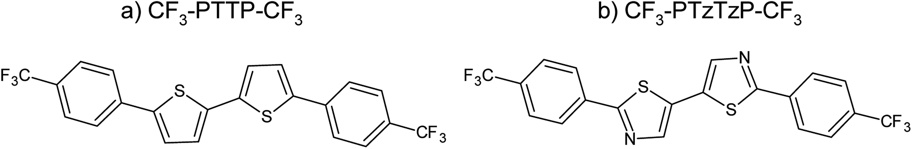
| Fig. 2 Equilibrium geometries, HOMO (a and b) and LUMO (c and d) patterns, and electrostatic potential maps (e and f) for the compounds studied. | ||
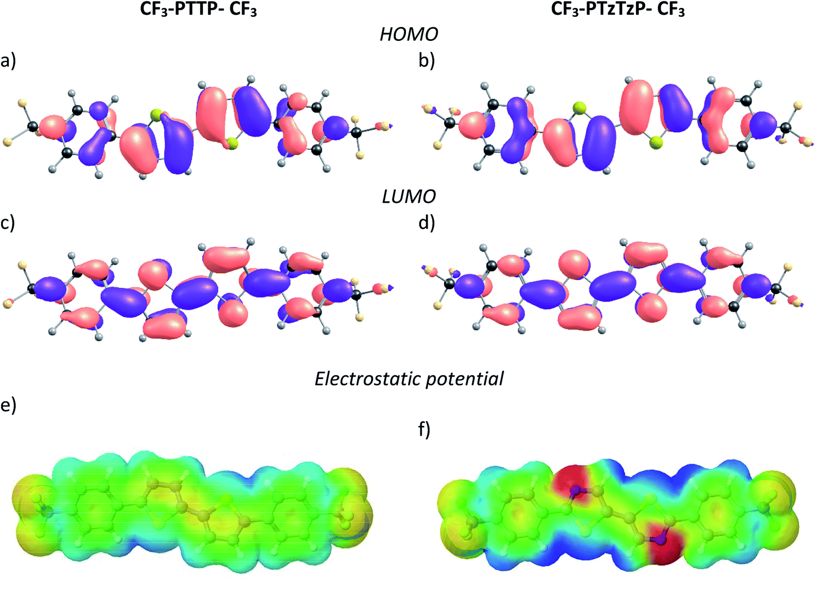
The HOMO and LUMO energies are presented in Table 1. The N-substitution results in a decrease of the HOMO and LUMO energies of CF3-PTTP-CF3 by 0.44 and 0.38 eV, respectively. The HOMO–LUMO gap, EHL, and optical gap, Eg, slightly widen with substitution, and the oscillator strength slightly decreases. These effects can be attributed to the slight decrease in the conjugation length from 6.65 Å for CF3-PTTP-CF3 to 6.59 Å for CF3-PTzTzP-CF3.
| HOMO | LUMO | EHL | Eg | f | |
|---|---|---|---|---|---|
| CF3-PTTP-CF3 | −5.45 | −2.13 | 3.32 | 3.055 | 1.34 |
| CF3-PTzTzP-CF3 | −5.89 | −2.51 | 3.39 | 3.091 | 1.28 |
 | ||
| Fig. 3 Absorption and photoluminescence spectra of CF3-PTTP-CF3 and CF3-PTzTzP-CF3 in THF solution. | ||
 | ||
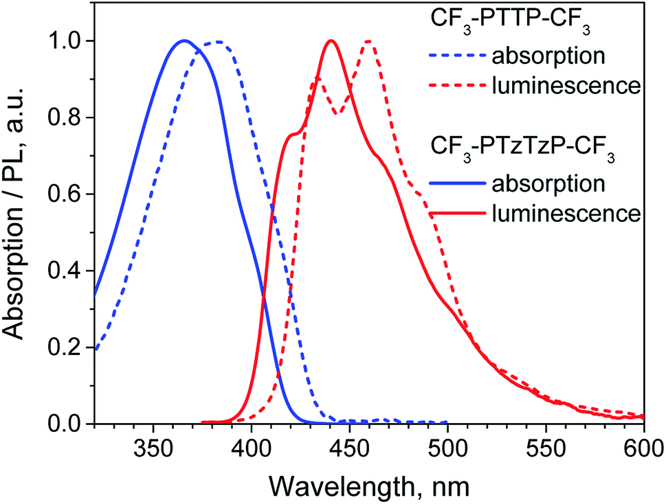
| Fig. 4 Experimental Raman spectra of polycrystalline powders of CF3-PTTP-CF3 (black) and CF3-PTzTzP-CF3 (red) normalized to the maximal intensity in the high-frequency range. Insets show the low-frequency (LF) range. Dashed blue lines indicate the positions of selected Raman bands of CF3-PTTP-CF3. | ||
3.2. Molecular and crystal structures
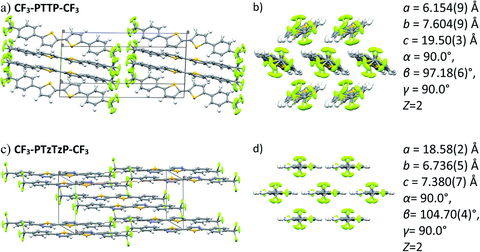 | ||
| Fig. 5 Crystal structures (two projections) for CF3-PTTP-CF3 (a and b) and CF3-PTzTzP-CF3 (c and d) and the corresponding unit cell parameters. | ||
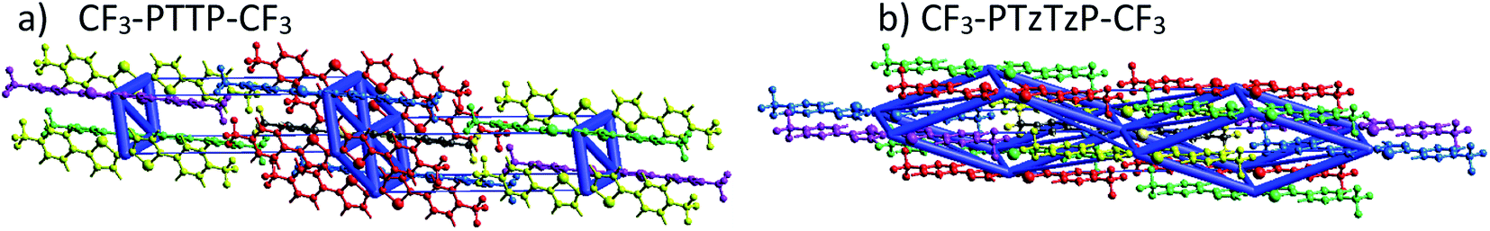 | ||
| Fig. 6 Graphical representation of the total interaction energy in blue on panel in CF3-PTTP-CF3 (a) and CF3-PTzTzP-CF3 (b) crystals. The cylinders link molecular centroids, and their thickness is proportional to the magnitude of the energy; for clarity, the pairwise energies with magnitudes less than 5 kJ mol−1 are not shown. Details are given in Table S1 and S2.†. | ||
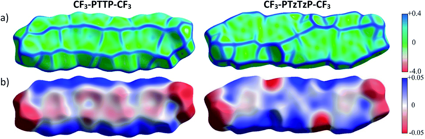 | ||
| Fig. 7 Hirshfeld surfaces of CF3-PTTP-CF3 and CF3-PTzTzP-CF3 mapped with curvature C (a) and ESP (±65.6 kJ mol−1 per unit charge) (b). | ||
Fig. 7(b) shows that the electrostatic potential of CF3-PTzTzP-CF3 differs from that of CF3-PTTP-CF3: whereas the thiophene rings in CF3-PTTP-CF3 generally have the electronegative center and the electropositive periphery (hydrogen atoms), the nitrogen atoms in thiazole rings of CF3-PTzTzP-CF3 pull out the electron density making the rest of the ring electropositive. This is in line with our calculations for isolated molecules (see Fig. 2(e and f)). As a result, in the CF3-PTzTzP-CF3 crystal, the thiazole rings always pack next to the phenylene rings, resulting in the ESP complementarity (Fig. S3†).55 Thus, we suggest that the abovementioned two-dimensional π-stacking observed in the CF3-PTzTzP-CF3 crystal is partially induced by the face-to-face electrostatic interactions between the N-substituted and non-substituted aromatic rings. In addition, the emergence of strongly electronegative areas at the edges of the molecule facilitates edge-to-edge interactions in the CF3-PTzTzP-CF3 crystal, which is indicated by formation of close edge-to-edge contacts (see Fig. S1†). As a result, we attribute the observed crossover from the herringbone packing in CF3-PTTP-CF3 to π-stacking in CF3-PTzTzP-CF3 to the fact that the face-to-face and edge-to-edge interactions (facilitating π-stacking) in the latter crystal overwhelm the edge-to-face interactions (facilitating herringbone packing).
Fig. 8 depicts the contributions of various atoms types to the intermolecular contacts in the crystals studied; the details of the analysis of the molecular contacts are given in ESI, Section S1.† As follows from this figure, the major contribution for CF3-PTTP-CF3 comes from C⋯H (typical for herringbone packing), F⋯F (because of the layered structure) and F⋯H contacts (because of electrostatic attraction of these atoms). For CF3-PTzTzP-CF3, the main contribution also comes from F⋯H and C⋯H contacts; however, the percentage of the former contacts increases significantly as a result of the interpenetration of the molecules into adjacent layers, while the percentage of the latter contacts significantly decreases as a result of the disappearance of the herringbone structure. Importantly, for CF3-PTTP-CF3, the percentage of the “conducting” contacts, i.e., the contacts between the atoms bearing large HOMO and/or LUMO electron density (see Fig. 2), is just 4% and stems from S–C and S–S contacts. On the contrary, for CF3-PTzTzP-CF3, this percentage increases to 13% and stems from C–C and N–C contacts. The increase in the “conducting” contacts number (C⋯C, S⋯C, S⋯S, N⋯C, N⋯S, N⋯N) with the N-substitution should be attributed to the change in the packing motif from the herringbone one (CF3-PTTP-CF3) to brickwall packing (CF3-PTzTzP-CF3), in line with Fig. 4(a) and ES1.† This increase is favorable for charge transport as discussed below.
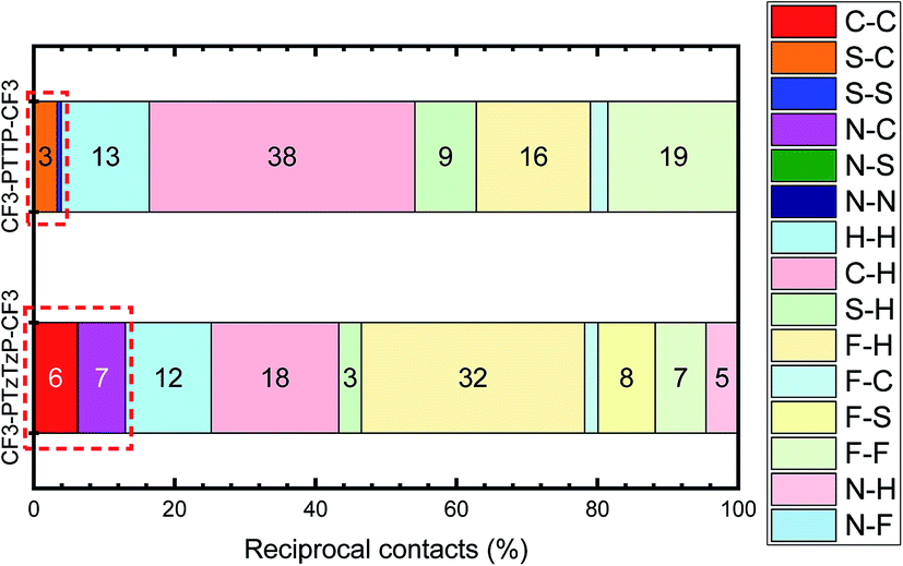 | ||
| Fig. 8 Distribution of intermolecular contacts for CF3-PTTP-CF3 and CF3-PTzTzP-CF3 arranged by molecules on the basis of Hirshfeld surface analysis. “Conducting” contacts (see details in the text) are highlighted with the dashed frames. | ||
3.3. Charge transport
 | (1) |
 | (2) |
 is the probability of the charge carrier to move in this direction. As follows from eqn (1) and (2), the higher the Ji and ri values and the lower the λ values, the larger the μ values.
The calculated reorganization energy for electron transfer, λ, is 420 meV for CF3-PTTP-CF3 and 320 meV for CF3-PTzTzP-CF3; these values correspond well with the results of previous works.26,44 Thus, the N-substitution significantly decreases λ, and this is beneficial for charge transport. The decrease of λ in CF3-PTzTzP-CF3 can be attributed the elimination of repulsion between the hydrogen atoms of the thiophene and phenylene rings (which torsionally distorts the conjugated core in CF3-PTTP-CF3) leading to planarization of the conjugated core and restriction of torsional degrees of freedom, which significantly contribute to the reorganization energy of thiohene-phenylene co-oligomers.62
Fig. 9 presents the charge transfer integrals, J, for the two crystals. In CF3-PTTP-CF3, there is a single direction with large J ∼ 80 meV; there are also two directions with J ∼ 20 meV. For CF3-PTzTzP-CF3, there are two directions with J ∼ 70 meV and one direction with J ∼ 20 meV. Since it is frequently assumed that the charge transport is efficient if J exceeds the energy of thermal fluctuations (25 meV at room temperature), in the latter crystal, the charge transport is quasi-two-dimensional, whereas in the former it is quasi-one-dimensional. The increase in the charge transport dimensionality can be favorable for μ.63 Moreover, in CF3-PTzTzP-CF3, high J are observed for directions with large ri, which is also beneficial for charge transport (see eqn (2) and Table S3†). Noteworthily, in both crystals, the efficient charge transport should occur exclusively within the layers (see Fig. 5 and 6; note that layered structure differs for the two crystals). This is reasonable since intralayer intermolecular interactions are much stronger than the interlayer ones (see Fig. S5†).
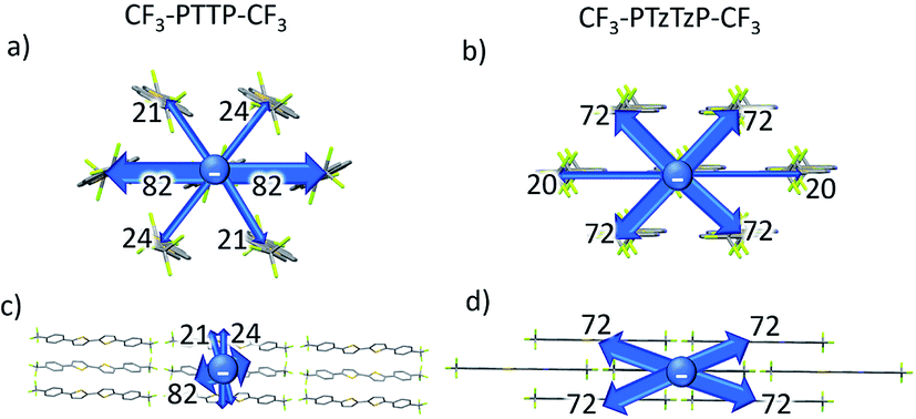 | ||
| Fig. 9 Charge transfer integrals, J, for CF3-PTTP-CF3 and CF3-PTzTzP-CF3; the J values are labeled. The thickness of the arrows illustrates the J magnitude. | ||
The μe values calculated using eqn (1) with the abovementioned J and λ are 0.065 cm2 V−1 s−1 for CF3-PTTP-CF3 and 0.43 cm2 V−1 s−1 for CF3-PTzTzP-CF3. Thus, the N-substitution results in about one order of magnitude increase in μe, in line with earlier calculations27 and experimental23,24 data. The hole mobility increases as well from 0.0047 cm2 V−1 s−1 in CF3-PTTP-CF3 to 0.43 cm2 V−1 s−1 in CF3-PTzTzP-CF3; however, the experimental data for hole transport in these materials are unavailable. The μe increase with the N-substitution can be attributed to the two factors: decrease in λ and increase in the Ji values for the directions with large ri.
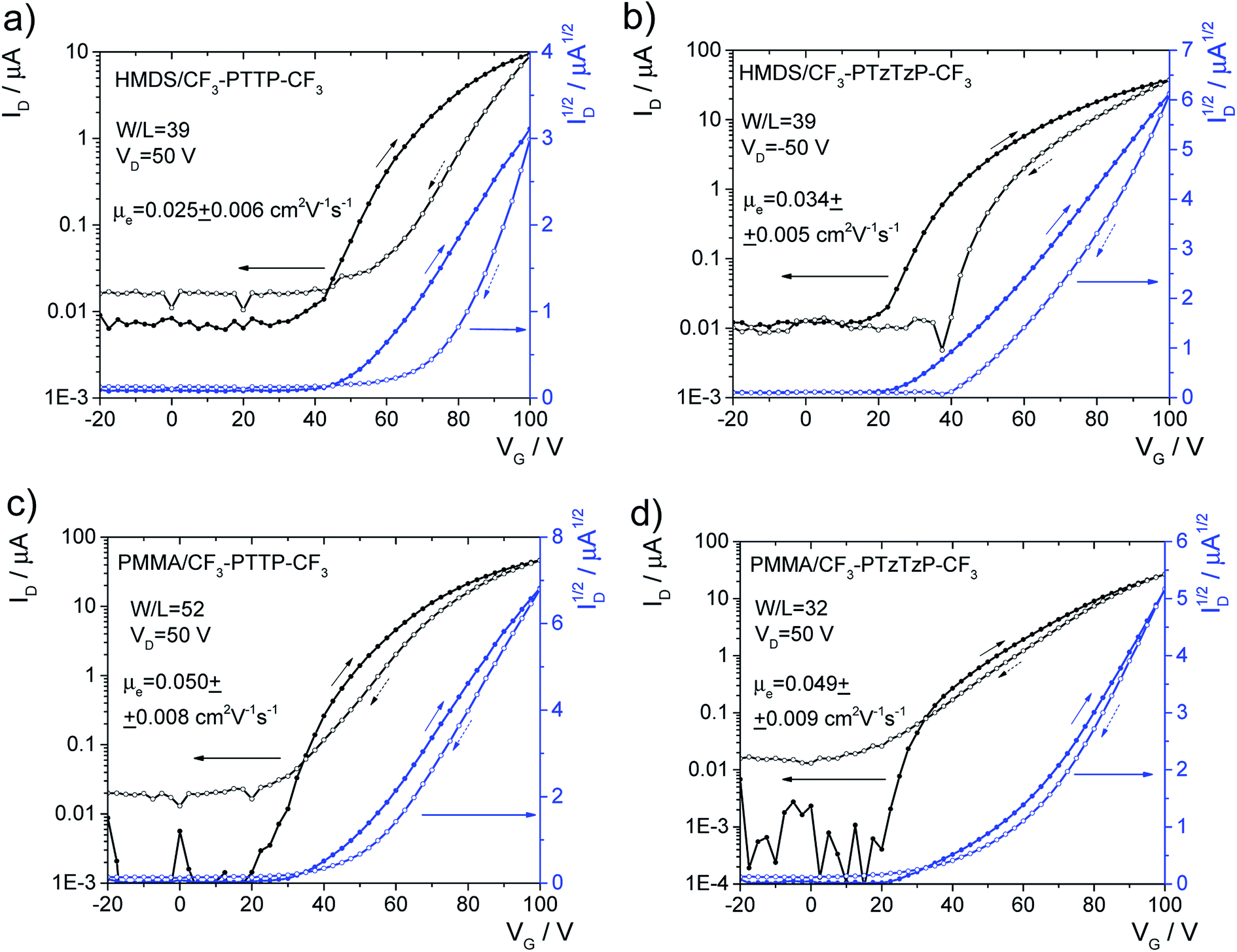 | ||
| Fig. 10 Typical transfer characteristics of OFETs based on CF3-PTTP-CF3 (a and c) and CF3-PTzTzP-CF3 (b and d) with HMDS (a and b) and PMMA (c and d) dielectric layers. Mobilities are shown for the backward direction of measurement, as their values are higher than for the forward direction. | ||
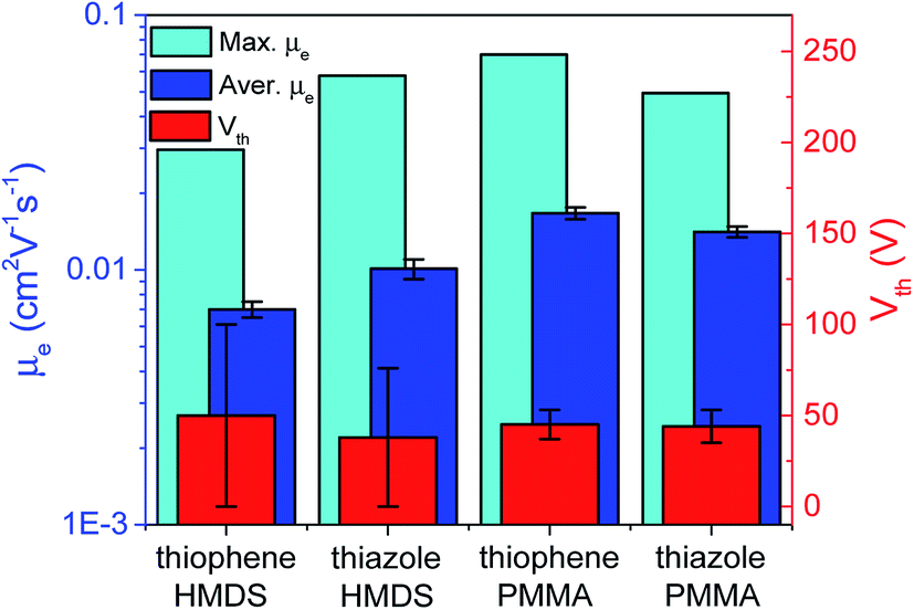 | ||
| Fig. 11 Maximal and average electron mobilities and average threshold voltages for all prepared devices with HMDS or PMMA layers based on thiophene-containing (CF3-PTTP-CF3) and thiazole-containing (CF3-PTzTzP-CF3) oligomers. | ||
Finally, we assessed the optoelectronic performance of both oligomers, namely, electroluminescence and photoelectric effect in OFETs. Though the fabricated OFETs were unipolar, with the only one type of charge carriers are present in the channel (electrons), light emission is suggested to originate from charge recombination at (or near) the interface between the organic semiconductor and the electrode (source or drain), which injects the minor charge carriers (holes).64 Similarly the photoelectric effect in such devices can occur near the one electrode.65 Electroluminescence was observed in OFETs based on both oligomers and its intensity was 2.5 times higher in the N-substituted oligomer. OFET images taken during the current characteristics measurements and other details are given in Fig. S13.† For both oligomers, a comparable photoelectric effect was observed so that the drain current exhibited an enhancement up to ∼30% depending on VG under illumination by a white LED (Fig. S14†). In summary, the thin-film OFETs based on the two oligomers showed comparable charge-transport properties, electroluminescence intensity, and photoelectric effect.
3.4. Comparison of N-substitution and fluorination of thiophene–phenylene co-oligomers
It is instructive to compare the impact of the N-substitution on various properties of CF3-PTTP-CF3 with the effect of fluorination on the properties of the another thiophene–phenylene co-oligomer PTPTP (P and T stand for phenyl(ene) and thiophene, respectively), which was recently reported in ref. 16. Both series of oligomers have been investigated as active layers of OFETs and OLETs and have shown promising characteristics. In both cases, electronegative atoms (N or F) are introduced into the molecule resulting in a dramatic change of the electrostatic potential (see Fig. 2(e–f) and ref. 16). The difference between the fluorination and N-substitution is that in the former case, peripherical atoms that are not significantly involved into the π-conjugation are substituted, while in the latter case, the very interior of the conjugated core is altered. In the following, we briefly compare the impact of the two substitution strategies on the HOMO/LUMO energies, optical properties, Raman spectra, crystal structure, and electron transport.Both type of substitution resulted in planarization of the molecules induced by the elimination of the repulsion of the hydrogen atoms from the adjacent thiophene and phenyl(ene) rings. Introduction of 4, 10, and 14 fluorine atoms into the PTPTP molecule resulted in the decrease of its theoretical HOMO (LUMO) by 0.2 (0.35), 0.4 (0.5) and 0.6 (0.8) eV, correspondingly. Similarly, the N-substitution via replacement of just two N atoms in CF3-PTTP-CF3 resulted in the decrease of theoretical HOMO (LUMO) by 0.4 (0.4) eV. The stronger effect of the N-substitution can be attributed to the higher π-electron density at the substituted atoms as mentioned in Section 3.1.1. The optical properties also varied in a similar way: both the F- and N-substitution resulted in the blueshift of absorption and emission spectra (see Fig. 8 and ref. 16). The PLQY in diluted solutions did not change significantly with the substitution. The changes of the Raman spectra revealed the difference in the position of substitution: in the PTPTP series, the phenyl(ene)-associated modes are shifted since the phenyl(ene) rings are fluorinated, whereas in the CF3-PTTP-CF3/CF3-PTzTzP-CF3 pair, the thiophene-associated modes are altered since the thiophene rings were converted into the thiazole ones.
In both series, the substitution resulted in the change of the crystal structure from herringbone motif to π-stacking. This is in line with the widely observed transition to π-stacking as a result of substitution with electronegative atoms (e.g. N, F, Cl, etc.).7,15,66–68 For instance, whereas bithiophenes pack in a herringbone motif, bithiazoles pack in a π-stacking manner.28 The intra-ring N-substitution of oligoacenes also results in the crossover to the π-stacking structure.69 These changes can be explained by the changes in the molecular electrostatics: the mentioned atoms in the molecular structure bear a negative charge, which attracts positively charged hydrogen and carbon atoms of the adjacent molecules stabilizing the face-to-face and edge-to-edge molecular interaction and hindering C⋯H contacts, which are dominant in herringbone packings (Fig. 5). As a result, these rings stack preferentially with the non-substituted rings.
The similar changes in the crystal structure for both series—crossover from herringbone packing to π-stacking with substitution—reveal themselves in the similar changes in the LF Raman spectra, which are very sensitive to the molecular interactions.47,56,57 Specifically, the LF Raman spectra in both CF3-PTzTzP-CF3 and fluorinated PTPTP (PFTPFTPF, PF stands for fluorinated phenyl(ene)) have much lower intensity (relative to the high-frequency part) than that in CF3-PTTP-CF3 and PTPTP (see Fig. S8†). Since the Raman intensity is associated with vibrational modulation of the material polarizability,47,70,71 a decrease of the LF Raman intensity can be attributed to a weaker impact of the corresponding vibrations on the charge-transfer integrals between the molecules and intramolecular charge delocalization, which determine the OSs polarizability. This decrease is expected to be favorable for charge transport.46,47,59,60 Thus, the fluorination and N-substitution not just increase the charge-transfer integrals but also inhibit their vibrational modulation.
The abovementioned similar changes in the crystal structure also result in similar changes in the electron transport pathways. Specifically, in both CF3-PTTP-CF3 and PTPTP crystals, electron transfer integrals are large only in one direction – where the molecules are arranged in a parallel manner. On the contrary, in the crystals of CF3-PTzTzP-CF3 and fluorinated PTPTP (PFTPTPF, and PFTPFTPF) these integrals are considerable in two directions. As a result, the charge transport changes from quasi-one-dimensional to quasi-two-dimensional, which can increase the charge mobility and make it less susceptible to defects.45 Whether the increase of the charge transport dimensionality is a general effect of electronegative substitution is a subject of further studies.
4. Conclusions
We addressed computationally and experimentally the impact of substitution of two C–H atom pairs with N atoms in the thiophene ring of a thiophene–phenylene co-oligomer on its properties. The crossover from the herringbone packing motif to π-stacking as a result of N-substitution was explained by the changes in the molecular electrostatic potential and formation of strongly electronegative areas. The Raman spectra indicated the frequency shift for the high-frequency vibrational modes with dominant contribution from the motion of thiophene/thiazole rings, while the modes associated mostly with phenylene rings vibrations were nearly unaffected. The low-frequency part of the Raman spectra was suppressed with the N-substitution, which can be attributed to the suppression of thermal fluctuation of the charge-transfer integrals. The theoretical charge mobility for N-substituted oligomer was found considerably higher than that for unsubstituted one; this was attributed to the large charge transfer integrals in the directions with large distance between the centers of adjacent molecules and decrease in the reorganization energy. Thin films of both oligomers demonstrated in OFET only electron transport with comparable charge-carrier mobilities, electroluminescence intensities, and photoelectric effect. An intriguing similarity between the effects of N-substitution and fluorination of thiophene–phenylene oligomers was revealed, which is probably a part of more general effect of electronegative substitution. The obtained results are anticipated to be an important contribution into the investigation of the structure–property relationships for organic semiconductors that will stimulate the rational design of these materials.Conflicts of interest
There are no conflicts to declare.Acknowledgements
Fabrication and studies of OFETs were supported by Russian Science Foundation (project #18-79-00341). Computational study of molecular properties and charge transport, as well as experimental studies of Raman spectra were supported by Russian Science Foundation (project #18-72-10165). Theoretical analysis of the crystal structures was performed with the support from the Foundation for the advancement of theoretical physics and mathematics “BASIS”. UV/vis spectroscopy and fluorescence measurements in solution were performed with financial support from the Ministry of Science and Higher Education of the Russian Federation, using the equipment of the Collaborative Access Center “Center for Polymer Research” of ISPM RAS. Experimental Raman and OFET studies were conducted using the equipment purchased under the Lomonosov Moscow State University Program of Development.References
- S. Reineke, M. Thomschke, B. Lussem and K. Leo, Rev. Mod. Phys., 2013, 85, 1245 CrossRef CAS.
- S. Toffanin, R. Capelli, W. Koopman, G. Generali, S. Cavallini, A. Stefani, D. Saguatti, G. Ruani and M. Muccini, Laser Photonics Rev., 2013, 7, 1011 CrossRef CAS.
- A. J. Kuehne and M. C. Gather, Chem. Rev., 2016, 116, 12823 CrossRef CAS PubMed.
- A. R. Murphy and J. M. Frechet, Chem. Rev., 2007, 107, 1066 CrossRef CAS PubMed.
- K. J. Baeg, M. Binda, D. Natali, M. Caironi and Y. Y. Noh, Adv. Mater., 2012, 25, 4267 CrossRef PubMed.
- A. V. Monika, M. K. Tiwari, B. Show and S. Saha, ACS Omega, 2020, 5, 448 CrossRef PubMed.
- Y. Krupskaya, M. Gibertini, N. Marzari and A. F. Morpurgo, Adv. Mater., 2015, 27, 2453 CrossRef CAS PubMed.
- J. H. Dou, Y. Q. Zheng, Z. F. Yao, Z. A. Yu, T. Lei, X. X. Shen, X. Y. Luo, J. L. Sun, S. D. Zhang, Y. F. Ding, G. C. Han, Y. P. Yi, J. Y. Wang and J. Pei, J. Am. Chem. Soc., 2015, 137, 15947 CrossRef CAS PubMed.
- B. Milian-Medina and J. Gierschner, J. Phys. Chem. Lett., 2017, 8, 91 CrossRef CAS PubMed.
- M. Tang and Z. Bao, Chem. Mater., 2011, 23, 446 CrossRef CAS.
- H. Adams, J.-L. J. Blanco, G. Chessari, C. A. Hunter, C. M. R. Low, J. M. Sanderson and J. G. Vinter, Chem.–Eur. J., 2001, 7, 3494 CrossRef CAS.
- S. Subramanian, S. K. Park, S. R. Parkin, V. Podzorov, T. N. Jackson and J. E. Anthony, J. Am. Chem. Soc., 2008, 130, 2706 CrossRef CAS PubMed.
- Z.-F. Yao, J.-Y. Wang and J. Pei, Cryst. Growth Des., 2018, 18, 7 CrossRef CAS.
- J. Gierschner, M. Ehni, H. J. Egelhaaf, B. Milián Medina, D. Beljonne, H. Benmansour and G. C. Bazan, J. Chem. Phys., 2005, 123, 144914 CrossRef PubMed.
- M.-H. Yoon, A. Facchetti, C. E. Stern and T. J. Marks, J. Am. Chem. Soc., 2006, 128, 5792 CrossRef CAS PubMed.
- A. Y. Sosorev, V. A. Trukhanov, D. R. Maslennikov, O. V. Borshchev, R. A. Polyakov, M. S. Skorotetcky, N. M. Surin, M. S. Kazantsev, D. I. Dominskiy, V. A. Tafeenko, S. A. Ponomarenko and D. Y. Paraschuk, ACS Appl. Mater. Interfaces, 2020, 12, 9507 CrossRef CAS PubMed.
- E. A. Komissarova, D. I. Dominskiy, V. E. Zhulanov, G. G. Abashev, A. Siddiqui, S. P. Singh, A. Y. Sosorev and D. Y. Paraschuk, Phys. Chem. Chem. Phys., 2020, 22, 1665 RSC.
- H. E. Katz, A. J. Lovinger, J. Johnson, C. Kloc, T. Siegrist, W. Li, Y. Y. Lin and A. Dodabalapur, Nature, 2000, 404, 478 CrossRef CAS PubMed.
- A. F. Lv, Y. Li, W. Yue, L. Jiang, H. L. Dong, G. Y. Zhao, Q. Meng, W. Jiang, Y. D. He, Z. B. Li, Z. H. Wang and W. P. Hu, Chem. Commun., 2012, 48, 5154 RSC.
- A. Y. Sosorev, M. K. Nuraliev, E. V. Feldman, D. R. Maslennikov, O. V. Borshchev, M. S. Skorotetcky, N. M. Surin, M. S. Kazantsev, S. A. Ponomarenko and D. Y. Paraschuk, Phys. Chem. Chem. Phys., 2019, 21, 11578 RSC.
- Q. Miao, Adv. Mater., 2014, 26, 5541 CrossRef CAS PubMed.
- Z. X. Liang, Q. Tang, J. B. Xu and Q. A. Miao, Adv. Mater., 2011, 23, 1535 CrossRef CAS PubMed.
- S. Ando, R. Murakami, J. Nishida, H. Tada, Y. Inoue, S. Tokito and Y. Yamashita, J. Am. Chem. Soc., 2005, 127, 14996 CrossRef CAS PubMed.
- S. Ando, J. Nishida, H. Tada, Y. Inoue, S. Tokito and Y. Yamashita, J. Am. Chem. Soc., 2005, 127, 5336 CrossRef CAS PubMed.
- O. Ostroverkhova, Chem. Rev., 2016, 116, 13279 CrossRef CAS PubMed.
- K. Navamani, G. Saranya, P. Kolandaivel and K. Senthilkumar, Phys. Chem. Chem. Phys., 2013, 15, 17947 RSC.
- I. Yavuz, S. A. Lopez, J. B. Lin and K. N. Houk, J. Mater. Chem. C, 2016, 4, 11238 RSC.
- M. D. Curtis, J. Cao and J. W. Kampf, J. Am. Chem. Soc., 2004, 126, 4318 CrossRef CAS PubMed.
- A. Pron, P. Gawrys, M. Zagorska, D. Djurado and R. Demadrille, Chem. Soc. Rev., 2010, 39, 2577 RSC.
- M. W. Schmidt, K. K. Baldridge, J. A. Boatz, S. T. Elbert, M. S. Gordon, J. H. Jensen, S. Koseki, N. Matsunaga, K. A. Nguyen, S. Su, T. L. Windus, M. Dupuis and J. A. Montgomery, J. Comput. Chem., 1993, 14, 1347 CrossRef CAS.
- M. S. Gordon and M. W. Schmidt, Theory and Applications of Computational Chemistry: the first forty years, ed. C. E. Dykstra, G. Frenking, K. S. Kim and G. E. Scuseria, Elsevier, Amsterdam, 2005 Search PubMed.
- V. Coropceanu, J. Cornil, D. A. da Silva, Y. Olivier, R. Silbey and J.-L. Brédas, Chem. Rev., 2007, 107, 926 CrossRef CAS PubMed.
- Y. Li, V. Coropceanu and J.-L. Brédas, The WSPC Reference on Organic Electronics: Organic Semiconductors, ed. J.-L. Brédas and S. R. Marder, World Scientific, Singapore, 2016 Search PubMed.
- B. Baumeier, J. Kirkpatrick and D. Andrienko, Phys. Chem. Chem. Phys., 2010, 12, 11103 RSC.
- J. Kirkpatrick, Int. J. Quantum Chem., 2008, 108, 51 CrossRef CAS.
- H. Kobayashi, N. Kobayashi, S. Hosoi, N. Koshitani, D. Murakami, R. Shirasawa, Y. Kudo and D. Hobara, J. Chem. Phys., 2013, 139, 014707 CrossRef PubMed.
- Jmol: an open-source Java viewer for chemical structures in 3D, http://www.jmol.org/ Search PubMed.
- Chemcraft – graphical software for visualization of quantum chemistry computations, http://www.chemcraftprog.com Search PubMed.
- M. J. Turner, J. J. McKinnon, S. K. Wolff, D. J. Grimwood, P. R. Spackman, D. Jayatilaka and M. A. Spackman, CrystalExplorer17, 2017, University of Western Australia, http://www.hirshfeldsurface.net Search PubMed.
- C. F. Mackenzie, P. R. Spackman, D. Jayatilaka and M. A. Spackman, IUCrJ, 2017, 4, 575 CrossRef CAS PubMed.
- V. A. Postnikov, Y. I. Odarchenko, A. V. Iovlev, V. V. Bruevich, A. Y. Pereverzev, L. G. Kudryashova, V. V. Sobornov, L. Vidal, D. Chernyshov, Y. N. Luponosov, O. V. Borshchev, N. M. Surin, S. A. Ponomarenko, D. A. Ivanov and D. Y. Paraschuk, Cryst. Growth Des., 2014, 14, 1726 CrossRef CAS.
- E. A. Shumilkina, O. V. Borshchev, S. A. Ponomarenko, N. M. Surin, A. P. Pleshkova and A. M. Muzafarov, Mendeleev Commun., 2007, 17, 34 CrossRef CAS.
- G. A. Crosby and J. N. Demas, J. Phys. Chem., 1971, 75, 991 CrossRef CAS.
- S. A. Siddiqui, A. Al-Hajry and M. S. Al-Assiri, Int. J. Quantum Chem., 2016, 16, 339 CrossRef.
- J. Gierschner and S. Y. Park, J. Mater. Chem. C, 2013, 1, 5818 RSC.
- A. Y. Sosorev, D. R. Maslennikov, O. G. Kharlanov, I. Y. Chernyshov, V. V. Bruevich and D. Y. Paraschuk, Phys. Status Solidi RRL, 2019, 13, 1800485 Search PubMed.
- A. Y. Sosorev, I. Y. Chernyshov, D. Y. Paraschuk and M. V. Vener, in Molecular Spectroscopy, ed. Y. Ozaki, M. J. Wójcik and J. Popp, Wiley, 2019, ch. 15, pp. 425–458 Search PubMed.
- S. Ando, J. Nishida, H. Tada, Y. Inoue, S. Tokito and Y. Yamashita, CCDC 1427491: Experimental Crystal Structure Determination, 2015, DOI:10.5517/cc1jxf3z.
- S. Ando, R. Murakami, J. Nishida, H. Tada, Y. Inoue, S. Tokito and Y. Yamashita, CCDC 291639: Experimental Crystal Structure Determination, 2006, DOI:10.5517/cc9sgq7.
- M. Y. Chen, L. J. Yan, Y. Zhao, I. Murtaza, H. Meng and W. Huang, J. Mater. Chem. C, 2018, 6, 7416 RSC.
- G. Gryn'ova, K. H. Lin and C. Corminboeuf, J. Am. Chem. Soc., 2018, 140, 16370 CrossRef PubMed.
- J. J. McKinnon, M. A. Spackman and A. S. Mitchell, Acta Crystallogr., Sect. B: Struct. Sci., 2004, 60, 627 CrossRef PubMed.
- M. A. Spackman and P. Byrom, Chem. Phys. Lett., 1997, 267, 215 CrossRef CAS.
- M. A. Spackman and J. J. McKinnon, CrystEngComm, 2002, 4, 378 RSC.
- A. J. Edwards, C. F. Mackenzie, P. R. Spackman, D. Jayatilaka and M. A. Spackman, Faraday Discuss., 2017, 203, 93 RSC.
- A. Brillante, I. Bilotti, R. G. Della Valle, E. Venuti and A. Girlando, CrystEngComm, 2008, 10, 937 RSC.
- A. Brillante, I. Bilotti, R. G. Della Valle, E. Venuti, M. Masino and A. Girlando, Adv. Mater., 2005, 17, 2549 CrossRef CAS.
- A. Y. Sosorev, D. R. Maslennikov, I. Y. Chernyshov, D. I. Dominskiy, V. V. Bruevich, M. V. Vener and D. Y. Paraschuk, Phys. Chem. Chem. Phys., 2018, 20, 18912 RSC.
- S. Fratini, D. Mayou and S. Ciuchi, Adv. Funct. Mater., 2016, 26, 2292 CrossRef CAS.
- G. Schweicher, Y. Olivier, V. Lemaur and Y. H. Geerts, Isr. J. Chem., 2014, 54, 595 CrossRef CAS.
- R. Marcus and N. Sutin, Biochim. Biophys. Acta, 1985, 811, 265–322 CrossRef CAS.
- A. Y. Sosorev, Moscow Univ. Phys. Bull., 2019, 74, 639 CrossRef.
- A. Y. Sosorev, Phys. Chem. Chem. Phys., 2017, 19, 25478 RSC.
- C.-F. Liu, X. Liu, W.-Y. Lai and W. Huang, Adv. Mater., 2018, 30, 1802466 CrossRef PubMed.
- K.-J. Baeg, M. Binda, D. Natali, M. Caironi and Y.-Y. Noh, Adv. Mater., 2013, 25, 4267–4295 CrossRef CAS PubMed.
- E. O. Levina, I. Y. Chernyshov, A. P. Voronin, L. N. Alekseiko, A. I. Stash and M. V. Vener, RSC Adv., 2019, 9, 12520 RSC.
- X. P. Cui, C. Y. Xiao, W. Jiang and Z. H. Wang, Chem.–Asian J., 2019, 14, 1443 CrossRef CAS PubMed.
- S. E. Koh, B. Delley, J. E. Medvedeva, A. Facchetti, A. J. Freeman, T. J. Marks and M. A. Ratner, J. Phys. Chem. B, 2006, 110, 24361 CrossRef CAS PubMed.
- K. E. Maly, Cryst. Growth Des., 2011, 11, 5628 CrossRef CAS.
- C. Ambrosch-Draxl, H. Auer, R. Kouba, E. Y. Sherman, P. Knoll and M. Mayer, Phys. Rev. B: Condens. Matter Mater. Phys., 2002, 65, 064501 CrossRef.
- R. Scholz, L. Gisslén, C. Himcinschi, I. Vragović, E. M. Calzado, E. Louis, E. S. Maroto and M. A. Díaz-García, J. Phys. Chem. A, 2009, 113, 315 CrossRef CAS PubMed.
Footnote |
| † Electronic supplementary information (ESI) available. See DOI: 10.1039/d0ra03343j |
| This journal is © The Royal Society of Chemistry 2020 |