
 Open Access Article
 This Open Access Article is licensed under a Creative Commons Attribution-Non Commercial 3.0 Unported Licence
A review of molybdenum disulfide (MoS2) based photodetectors: from ultra-broadband, self-powered to flexible devices
Hari Singh Nalwa

Advanced Technology Research, 26650 The Old Road, Valencia, California 91381, USA. E-mail: nalwa@mindspring.com
First published on 19th August 2020
Abstract
Two-dimensional transition metal dichalcogenides (2D TMDs) have attracted much attention in the field of optoelectronics due to their tunable bandgaps, strong interaction with light and tremendous capability for developing diverse van der Waals heterostructures (vdWHs) with other materials. Molybdenum disulfide (MoS2) atomic layers which exhibit high carrier mobility and optical transparency are very suitable for developing ultra-broadband photodetectors to be used from surveillance and healthcare to optical communication. This review provides a brief introduction to TMD-based photodetectors, exclusively focused on MoS2-based photodetectors. The current research advances show that the photoresponse of atomic layered MoS2 can be significantly improved by boosting its charge carrier mobility and incident light absorption via forming MoS2 based plasmonic nanostructures, halide perovskites–MoS2 heterostructures, 2D–0D MoS2/quantum dots (QDs) and 2D–2D MoS2 hybrid vdWHs, chemical doping, and surface functionalization of MoS2 atomic layers. By utilizing these different integration strategies, MoS2 hybrid heterostructure-based photodetectors exhibited remarkably high photoresponsivity raging from mA W−1 up to 1010 A W−1, detectivity from 107 to 1015 Jones and a photoresponse time from seconds (s) to nanoseconds (10−9 s), varying by several orders of magnitude from deep-ultraviolet (DUV) to the long-wavelength infrared (LWIR) region. The flexible photodetectors developed from MoS2-based hybrid heterostructures with graphene, carbon nanotubes (CNTs), TMDs, and ZnO are also discussed. In addition, strain-induced and self-powered MoS2 based photodetectors have also been summarized. The factors affecting the figure of merit of a very wide range of MoS2-based photodetectors have been analyzed in terms of their photoresponsivity, detectivity, response speed, and quantum efficiency along with their measurement wavelengths and incident laser power densities. Conclusions and the future direction are also outlined on the development of MoS2 and other 2D TMD-based photodetectors.
 Hari Singh Nalwa | Dr Hari Singh Nalwa is a distinguished independent scientist and scholar working in the fields of nanotechnology and materials science. Dr Nalwa has authored more than 170 scientific articles, 26 book chapters, and 125 volumes of scientific books, as well as 18 patents in cross-disciplinary research areas of nanotechnology, materials science and polymer science. Dr Nalwa's research interests include ferroelectric polymers, conducting polymers, organic nonlinear optical materials for integrated optics, low- and high-dielectric constant materials for microelectronics packaging, 3D printing, two-dimensional (2D) nanomaterial-based bulk heterojunction and dye-sensitized solar cells, and multifunctional sensors for wearable technology. He received the “Award of Excellence” from the Association of American Publishers for the “Handbook of Nanostructured Materials and Nanotechnology,” a 5-volume set (Academic Press, 2000), and “Best Reference Work Award” from the American Society for Engineering Education for “The Encyclopedia of Nanoscience and Nanotechnology,” a 10-volume set (American Scientific Publishers, 2004). He is Founder, President, and Chief Executive Officer (CEO) of American Scientific Publishers (http://www.aspbs.com), which he established in 2000. |
1. Introduction
Advances in the fields of electronics, optoelectronics and photonics have created a great demand for new functional materials that possess ease of synthesis, processing and fabrication and enable desired tailoring of the physical and chemical properties by chemical functionalization and/or formation of hybrid structures for potential applications in electronic and optoelectronic devices.1,2 In this context, earth-abundant two-dimensional (2D) nanomaterials, including graphene3–12 and transition metal dichalcogenides (TMDs),13–20 have emerged as novel functional materials of choice due to their low-cost production, easy processing and easy deposition on different substrates with precise thickness control of the atomic layers via mechanical and chemical exfoliation, chemical vapor deposition (CVD) and atomic layer etching (ALE) methods. Flexible graphene nanosheets have been explored for developing wearable and portable devices, including field-effect transistors (FETs),21,22 sensors,23–25 supercapacitors,26–28 lithium-ion batteries,29 triboelectric nanogenerators,30 solar cells31–33 and photodetectors.34,35 Following the research progress of graphene, a similar wide range of applications for flexible atomic layered TMDs have been anticipated and are now slowly emerging, from wearable electronics to optoelectronics.36–40 Flexible photodetectors are becoming a key component of optoelectronic technology for a wide range of applications in the fields of surveillance, soft robotics, sensors for wearable and portable healthcare and sports, light-emitting diodes (LEDs), high-speed optical communication, and biomedical imaging.34,35,41 Flexible photodetectors are gaining much attention for use in wearable optoelectronics, for which many different types of nanostructures, such as atomic layered nanosheets, nanowires (NWs), fibers, quantum dots and 3D networks of inorganic and organic materials and their nanohybrids, have been studied. These nanostructures have been used as phototransistors, photoconductors and photodiodes for developing photodetectors from a wide variety of nanomaterials, including silicon (Si) and germanium (Ge),42,43 selenium (Se),44 GaP and InP,45,46 CdS,47,48 ZnSe,49 ZnO and its hybrids with PbS, ZnS, CdO, gold (Au) and polymers,50–55 ZnGa2O4,56 Zn2GeO4 and In2Ge2O7,57 CuInSe2,58,59 In2S3,60 In2Se3,61 Sb2S3,62 Sb2Se3,63 Bi2S3,64 SnS,65 SnS2,66 ZrS3,67 Zn3P2,68 PbI2,69 MoO3,70 GaS,71 SnO2,72 ZnTe,73 GaTe,74 perovskites,75,76 their hybrid composites with ZnO, gold, poly(diketopyrrolopyrrole-terthiophene) (PDPP3T) conjugated polymer, and graphene,77–80 polythiophene,81 carbon nanotubes (CNTs),82 graphene nanocomposites with CNTs83 and with ZnO quantum dots,84 transition-metal trichalcogenides (MX3, where M represents a transition metal, Ti, Zr, Hf, Nb, or Ta, and X is a chalcogen, S, Se, or Te), e.g., hafnium trisulfide (HfS3),85 HfS3 and HfSe3 nanocomposites with graphene,86 and graphene-based materials.87–89 The important parameters including photoresponsivity, specific detectivity, noise equivalent power (NEP), photogain, external quantum efficiency (EQE), linear dynamic range (LDR), and response speed of photodetectors have already been well defined in the literature;1 here, these parameters are discussed in reference to the nanomaterial-based photodetectors and especially for the MoS2 atomic layer-based hybrid photodetectors.Many research articles have been published on atomically thin layered MoS2 based photodetectors, however, a comprehensive review summarizing the recent developments in MoS2 photodetectors is completely lacking in the scientific literature. This review briefly introduces TMDs, including the applications of MoS2 atomic layers in developing photodetectors. The tuning of optoelectronic properties by boosting the carrier mobility of and incident light absorption by MoS2 atomic layers through the use of plasmonic and halide perovskite–MoS2 hybrid heterostructures, 2D–0D and 2D–2D MoS2 heterostructures, interface coupling effect (ICE), or chemical doping of MoS2 films is discussed in order to evaluate the performance of MoS2 photodetectors from the perspective of their based phototransistors, photoconductors and photodiode components. Particular emphasis is placed on atomic layered MoS2-based ultra-broadband photodetectors, from their fundamental development to self-powered to flexible photodetectors for wearable optoelectronics. The performance of pristine MoS2 atomic layers and MoS2 hybrid heterostructures with graphene, CNTs, TMDs, ZnO and surface functionalized MoS2 atomic layers for developing flexible photodetectors is discussed in terms of their broadband photoresponsivity, detectivity, NEP, photogain, EQE, photoresponse speed, mechanical flexibility and environmental stability. Strain-induced and self-powered MoS2 based hybrid photodetectors has also been summarized. Finally, the challenges in developing flexible photodetectors from TMDs are analyzed. This review should be a useful source for and inspire a wide range of audience, including researchers working in the fields of optoelectronics, sensors, materials science, nanotechnology, physics, electrical engineering, and communications.
2. Molybdenum disulfide (MoS2) for photodetectors
Fig. 1 shows the wide range of the electromagnetic spectrum covered by 2D nanomaterials, from the near-infrared (NIR) and mid-IR (MIR) to the far-IR (FIR), the related applications of these nanomaterials in electronics, optoelectronics and photonics, and the atomic and band structures of 2D materials, including hexagonal boron nitride (h-BN), molybdenum disulfide (MoS2), black phosphorus (BP) and graphene.90 h-BN is an insulator with a large bandgap of 6.0 eV,91–95 whereas MoS2 96–98 and BP99–101 are semiconductors with sizeable bandgaps that vary with the number of atomic layers. Graphene is a zero bandgap semimetal102,103 and monolayer graphene exhibits 97.7% optical transparency independent of the optical wavelength in the 450–800 nm spectral region; the transparency decreases proportionally with an increasing number of graphene layers.104 Monolayer graphene absorbs only 2.3% of incident white light; therefore, the photoresponsivity of monolayer (1L) graphene is rather limited due to the low absorbance in the visible region. The insulating layers of an h-BN dielectric have been used along with other 2D materials, such as graphene, BP and TMDs, including MoS2, MoSe2, WS2, WSe2, MoTe2, etc., to develop electronic and optoelectronic devices.105–109 Though graphene-based materials have been extensively studied for use in photodetectors because of their high carrier mobility and strong interaction with light over a broad spectral range,110–113 graphene-based photodetectors suffer from low photoresponsivity due to graphene's weak optical absorption.104,114 Broadband photodetectors utilizing multilayer BP operating over the 532 nm to 3.39 μm wavelength range have been fabricated by Guo et al.115 Comparatively, TMDs have a large electronic density of states, giving rise to high optical absorption and ultrafast charge transfer, making them more suitable for photodetectors. Bernardi et al.116a reported 5–10% incident sunlight absorption by MoS2, MoSe2, and WS2 monolayers for a thickness of >1 nm, which is higher than the value of 2.3% exhibited by monolayer graphene104 and one order of magnitude higher than those of thin films of the conventional semiconductors GaAs and Si, generally used for solar energy applications. Fig. 2(a) compares the computed and measured absorbance of monolayer (1L) MoS2. The computed absorbance of 1L MoS2 was obtained using density functional theory (DFT) calculations, GW method and the Bethe–Salpeter equation (BSE) while experimental absorbance was reported by Mak et al.96 The quantitative agreement was observed between the computed and experimentally measured absorbance of 1L MoS2. Fig. 2(b) compares the optical absorbance of MoS2, MoSe2, and WS2 monolayers with that of graphene, clearly showing that TMD monolayers absorb much more sunlight than graphene. The calculated flux of absorbed photons was 4.6, 3.9, 2.3, and 2.0 mA cm−2 for monolayer MoSe2, MoS2, WS2 and graphene, respectively, compared with 0.3 mA cm−2 for GaAs and 0.1 mA cm−2 for Si in the form of 1 nm thin films. A monolayer TMD can absorb as much sunlight as a 50 nm thick Si film. Wang et al.116b summarized the band-gaps of different atomic layered 2D nanomaterials including MoS2, MoSe2, MoTe2, WS2, WSe2, ReS2, ReSe2, SnS2, SnSe2, HfS2, HfSe2, ZrS2, ZrSe2, In2Se3, black AsP, black phosphorus (BP), and h-BN with their corresponding photodetection range, varying from near ultraviolet (NUV) to long infrared (LIR) as shown in Fig. 2(c). MoS2, WSe2, SnS2, and black phosphorus show a broadband spectral range from NUV wavelength to mid-infrared (MIR) wavelength. The optical absorbance of MoS2 thin films can be further extended by developing diverse hybrid heterostructures.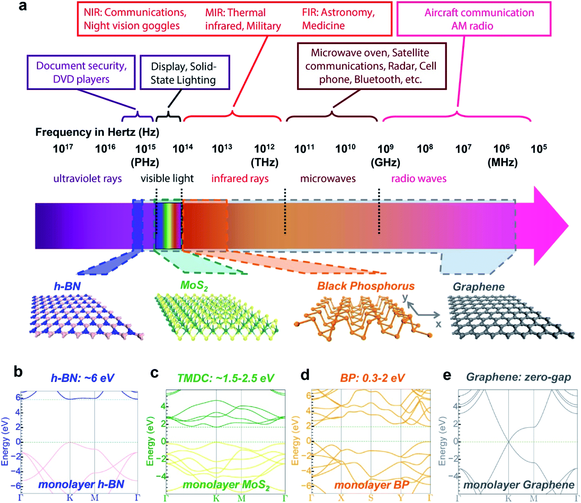 | ||
| Fig. 1 (a) 2D materials covering a very wide range of the electromagnetic spectrum, from the NIR and MIR to the FIR, and their corresponding applications. The bottom section shows the atomic structures of h-BN, MoS2, black phosphorus (BP) and graphene from left to right. The electromagnetic spectral ranges covered by different 2D materials are depicted using colored polygons. (b–e) Band structures and bandgaps of monolayer h-BN (b), MoS2 (c), BP (d) and gapless graphene (e). Reprinted with permission from ref. 90, copyright © 2014 Macmillan Publishers Limited. | ||
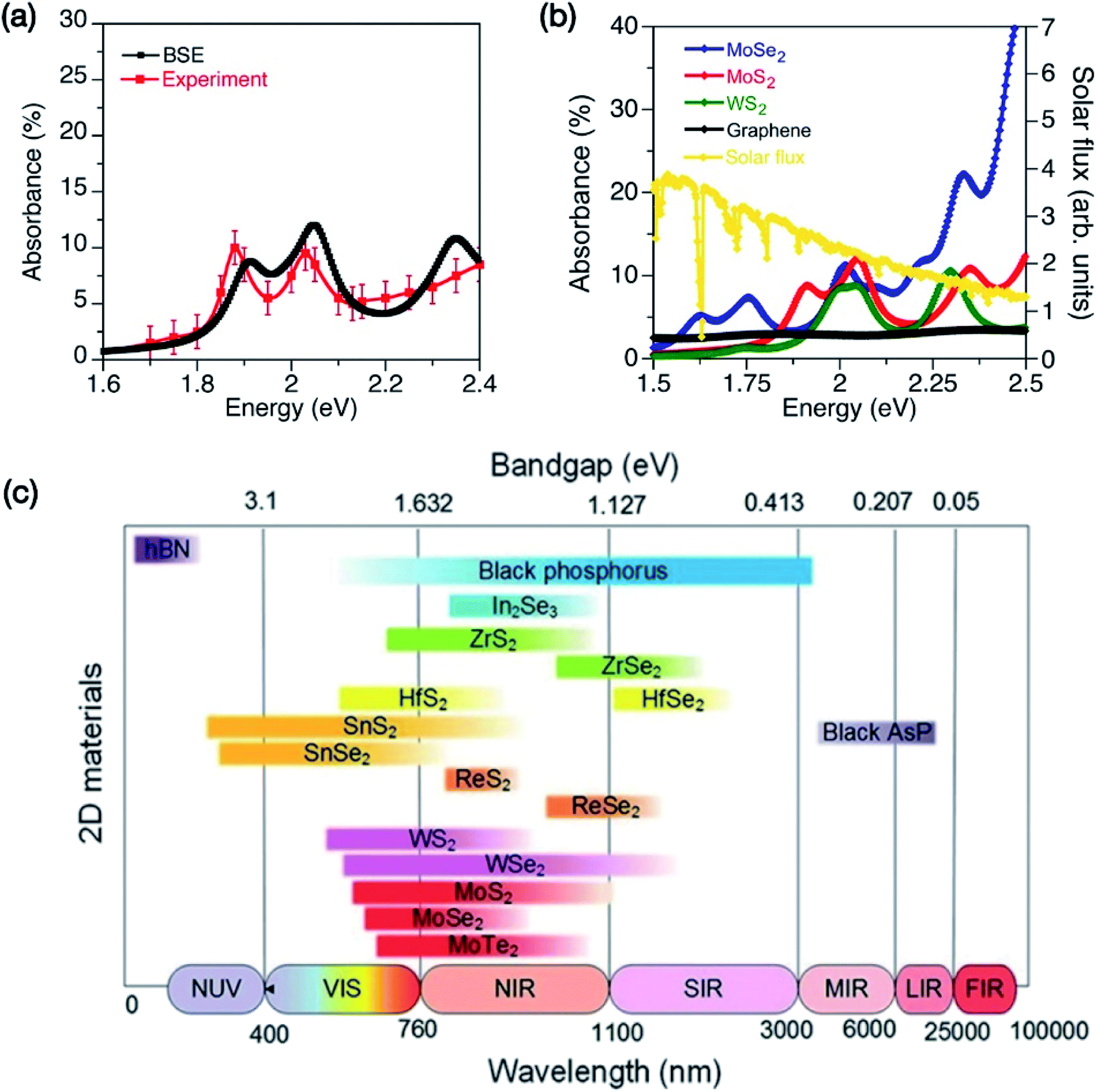 | ||
| Fig. 2 (a) A comparison of the computed absorbance obtained by Bethe–Salpeter equation (BSE) with experimentally measured absorbance of a MoS2 monolayer. (b) A comparison of the optical absorbance of MoS2, MoSe2, and WS2 monolayers with that of graphene along with the incident AM1.5G solar flux. Reprinted with permission from ref. 116a, copyright © American Chemical Society. (c) Band-gaps of different atomic layered 2D nanomaterials (MoS2, MoSe2, MoTe2, WS2, WSe2, ReS2, ReSe2, SnS2, SnSe2, HfS2, HfSe2, ZrS2, ZrSe2, In2Se3, black AsP, black phosphorus (BP) and h-BN) with their corresponding photodetection range varying from near ultraviolet (NUV) to long infrared (LIR). Reprinted with permission from ref. 116b, copyright © Wiley. | ||
The figure-of-merit for a photodetector is generally evaluated in terms of their photoresponsivity (R), specific detectivity (D*), noise equivalent power (NEP), and the photoresponse time. The photoresponsivity is an electrical response to an incident light illumination and detectivity is associated with the lowest required optical power intensity for a photodetector to differentiate signal from the actual noise. The intensities of dark and photo currents generated as a function of applied bias voltage and the values of photoresponsivity and detectivity at different operation wavelengths and optical power intensity are compared. The photoresponse rise and decay times are also measured to find out the speed of a photodetector. TMDs, such as MoS2, WS2, MoSe2, and WSe2, show a tunable bandgap that change from a direct bandgap in monolayers to an indirect bandgap in multilayers. Therefore, the optoelectronic properties of atomically thin layered TMDs can be tailored by utilizing their variable bandgaps and by improving the optical absorption by forming hybrid heterostructures. The large family of atomic layered TMDs is very attractive for their application in broadband photodetectors. For example, the internal quantum efficiency (IQE) of 85% for MoS2,117 IQE of 70% with an ultrafast photoresponse time of 5.5 ps for WSe2,118 IQE of 91% for WSe2/MoSe2 heterostructures,119 photoresponsivity of 2578 A W−1 for monolayer WSe2/nitrogen-doped graphene quantum dots (N-GQDs),120 ultrafast charge transfer of 50 fs for MoS2/WS2 heterostructures after photoexcitation,121 and, interestingly, photoresponsivity as high as 1 × 10¹⁰ A W−1 at 130 K and 5 × 10⁸ A W−1 at room temperature for a monolayer graphene/multilayer MoS2 hybrid structure illuminated at 632 nm with a power of 376 fW μm−2 with a response time of 1 × 10³ s,122 demonstrate the suitability of atomic layered TMDs for developing optoelectronic devices, including photodetectors,123,124 LEDs,125,126 and solar cells.127–132
The bandgap in TMDs can be adjusted by changing the number of layers, which allows tuning of the optical response over a broad range of wavelengths, from the ultraviolet (UV)-visible to NIR.133–135 Furthermore, the high carrier mobility and strong interaction of TMDs with light make these 2D materials interesting for optoelectronic applications. Atomically thin layered TMDs, including MoS2,136–140 MoSe2,141–144 MoTe2,145,146 WS2,147,148 WSe2/WS2,149 WSe2,120,150 WSe2/h-BN,151 HfS2,152,153 ReS2,154,155 ReSe2,156,157 SnS2,158,159 and WSe2/SnSe2,160 and the doped MoS2 heterostructures161 have been studied for use in broadband photodetectors. Among 2D TMDs, MoS2 atomic layers have also been extensively investigated for developing MoS2 hybrid heterostructure-based photodetectors in combination with other materials, including MoS2/Si,162 AuNPs/MoS2,163 MoS2/WS2,164 MoS2/WSe2,165 graphene/MoS2/WSe2/graphene,165 MoTe2/MoS2,166 GaTe/MoS2,167 PdSe2/MoS2,168 MoS2/graphene,169 and MoS2/BP.170 The formation of hybrid heterostructures with other materials facilitates the modification of electronic and optoelectronic properties in order to improve the photoresponse of MoS2-based photodetectors.
Several studies have demonstrated that the bandgap in MoS2 can be tuned by changing the number of layers (thickness), from 1.8 eV for monolayer MoS2 to 1.2 eV for multilayer MoS2.96–98 This strategy could be used to adjust the optical response of MoS2 over a broad spectral range. Mak et al.96 reported the strongest direct bandgap photoluminescence (PL) in monolayer (1L) MoS2, with 1000-fold enhancement of the PL intensity compared with bilayer (2L) MoS2 as well as strong emergence of photoconductivity near the direct bandgap of 1.8 eV in monolayer MoS2 and approximately 1.6 eV in bilayer MoS2. These results confirm the occurrence of an indirect to direct bandgap transition using photoconductivity spectroscopy. Fig. 3(a and b) shows a schematic illustration of monolayer and bilayer MoS2 on an atomic scale. In a bilayer (2L), MoS2 single layers are bound by van der Waals (vdW) forces having a nanoscale distance between the adjacent layers. Atomic layer MoS2 consisting of S–Mo–S atomic structures bonded through vdW forces show strong photodetection over a broad optical spectral range from the UV to IR. Lopez-Sanchez et al.171 reported a photoresponsivity of 880 A W−1 and a detectivity of 2.5 × 10¹⁰ Jones (Jones = cm Hz1/2 W−1) for monolayer MoS2 at a bias gate voltage (VBG) of −70 V and a Vds of 8 V for a 561 nm wavelength under a 150 pW incident power (2.4 × 10⁻¹ mW cm−2), along with a photoresponse in the 400–680 nm wavelength range, as shown in Fig. 3(c). CVD-grown monolayer MoS2 phototransistors exhibit a photoresponsivity as high as 2200 A W−1, a photogain of 5000 and a response time of 500 s at room temperature.172 Pang et al.173 developed a MoS2-based tribotronic phototransistor by combining a few-layer MoS2 phototransistor with a sliding mode triboelectric nanogenerator (TENG). The photoresponsivity of the MoS2 tribotronic phototransistor increased from 221.03 A W−1 to 727.87 A W−1 with increasing sliding distance from 0 mm to 8 mm under 10 mW cm−2 laser power intensity and a 1.0 V drain voltage. This result indicates that the photoresponsivity of the MoS2 phototransistor can be tuned by controlling the sliding distance, enabling self-powered photodetection with a TENG.
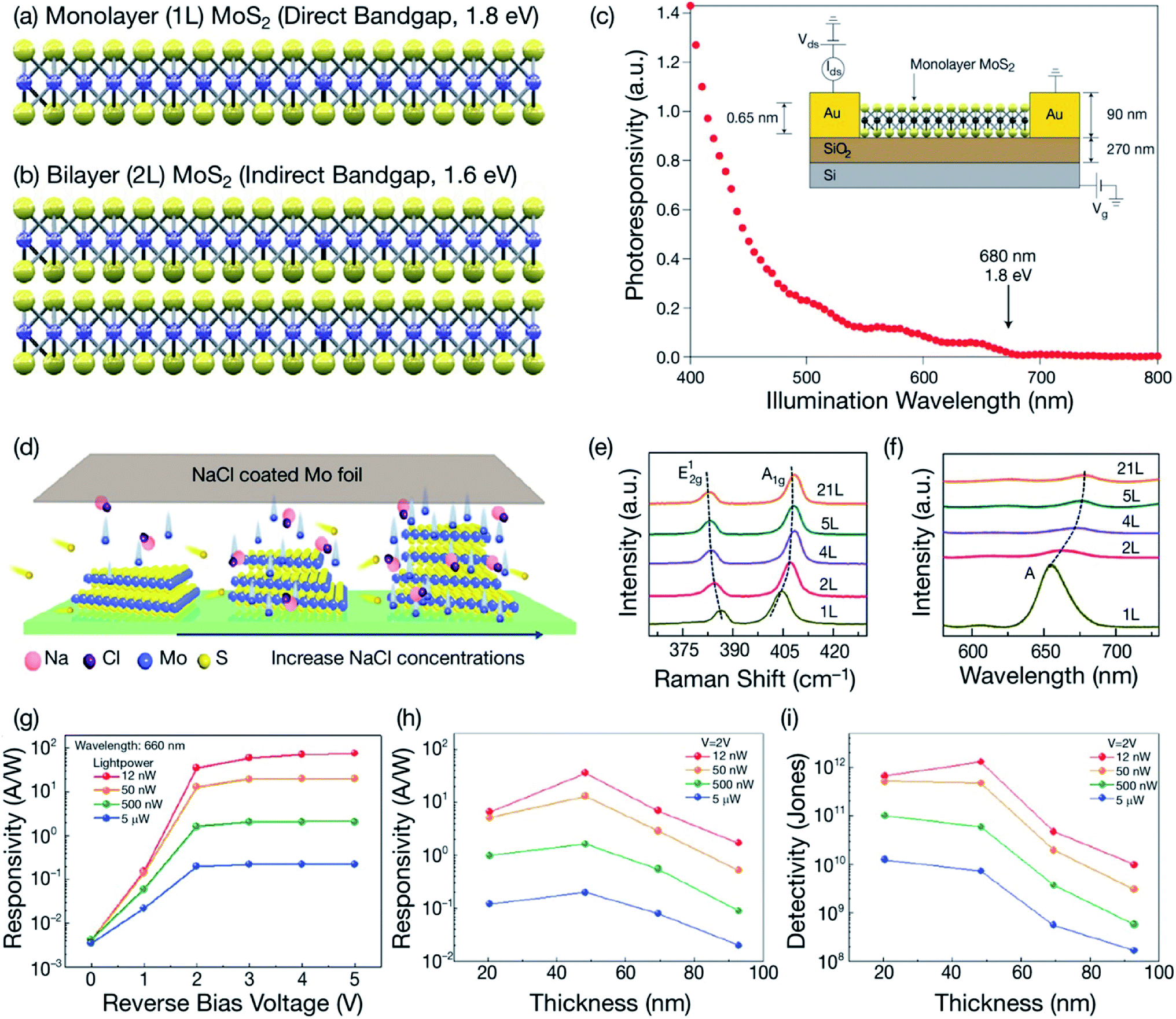 | ||
| Fig. 3 (a and b) Schematic illustration of monolayer and bilayer MoS2 on an atomic scale. The blue balls represent Mo atoms, while the yellow balls represent S atoms in MoS2. The direct bandgap of 1.8 eV observed in monolayer (1L) MoS2 transits to the indirect bandgap of 1.6 eV for bilayer (2L) MoS2 and to 1.2 eV for multilayer (ML) MoS2.96–98 In a bilayer (2L), MoS2 single layers are bound by van der Waals forces having a nanoscale distance between the adjacent layers. (c) Photoresponsivity of a monolayer MoS2 photodetector measured as a function of illumination wavelength in the 400 nm to 800 nm range. The photodetector shows an increasing photoresponsivity as the illumination wavelength is decreased from 680 nm to 400 nm. The monolayer MoS2-based photodetectors can be used over a broad spectral range. The inset shows the structural view of a monolayer (6.5 Å thick) MoS2 photodetector deposited on a back gate substrate with Au electrodes. Reprinted with permission from ref. 171, copyright © 2013 Macmillan Publishers Limited. (d) Schematic of NaCl-assisted layer-controlled low pressure CVD growth of MoS2 flakes. (e) Layer-dependent Raman spectra of MoS2 flakes showing the variation in the modes with increasing layer thickness. (f) Layer-dependent PL spectra of MoS2 flakes. Reprinted with permission from ref. 174, copyright © American Chemical Society. (g) Photoresponsivity of the MoS2/Si heterojunction photodetector as a function of reverse bias voltage at a 660 nm illumination wavelength under different incident laser powers. (h) Photoresponsivity of the MoS2/Si photodetector as a function of the thickness of MoS2 flakes at a bias voltage of 2.0 V under different incident powers. (i) Detectivity of the MoS2/Si photodetector as a function of the thickness of MoS2 flakes. Reprinted with permission from ref. 175, copyright © American Chemical Society. | ||
The number of MoS2 atomic layers also significantly affects the electronic and optoelectronic properties. Yang et al.174 reported the thickness-controlled growth of MoS2 using the NaCl-assisted low pressure CVD method, where the number of layers of MoS2 flakes was precisely controlled by simply increasing the concentration of the NaCl promoter. The Raman and PL spectra of 1L, 2L, 4L, 5L, and 21L MoS2 flakes showed an increase in the frequency difference (Δ) between the two characteristic Raman peaks (E2g1 and A1g vibration modes) from 18.3 to 25.7 cm−1 and a redshift in the PL peak from 655 nm to 678 nm as the MoS2 layer thicknesses increased from 1L to 21L (Fig. 3(d–f)). The intensity of the PL emission from MoS2 flakes decreased dramatically with increasing number of layers because of the direct to indirect bandgap transition, and similarly, the bandgap of MoS2 layers decreased with increasing layer thickness, from 1.8 eV for 1L to 1.5 eV for 2L and 1.2 eV for 25L. The optical transmittance measured at 550 nm gradually decreased with an increasing number of MoS2 layers, ranging from 85.0% to 57.7%, 50.1% and 24.8% for 1L, 2L, 5L and 21L MoS2. The UV-B absorptions of 1L, 2L, 5L and 21L MoS2 flakes were over 95%. The thickness-dependent optoelectronic properties of multilayer MoS2 have been studied. The highest values of photoresponsivity and detectivity reached 1 × 10⁴ A W−1 and 8 × 10¹² Jones for monolayer-bilayer (1L–2L) heterojunctions and 4 × 10³ A W−1 and 6 × 10¹² Jones for monolayer-8-layer (1L–8L) MoS2 heterojunctions at 660 nm.
In another study, Shin et al.175 deposited mechanically exfoliated multilayer MoS2 flakes onto a Si layer to develop MoS2/Si p–n heterojunction photodiodes; the optoelectronic properties were improved and optimized by controlling the number of layers of MoS2 flakes. The photoresponse of the MoS2/Si photodetector was measured at 405, 520, and 660 nm wavelengths under different incident power intensities and for various thicknesses of multilayer MoS2 flakes. The 2 nm thick MoS2 flake-based photodiodes showed very poor performance with low photoresponsivities of 3.36 × 10⁻³ and 6.64 × 10⁻⁵ A W−1 and detectivities of 2.08 × 10⁶ and 4.11 × 10⁵ Jones at a 660 nm wavelength under incident optical powers of 50 nW and 50 μW at 2 V, respectively. The thickness-dependent maximum values of the photoresponsivity and detectivity were obtained for 48 nm MoS2 flakes at 12 nW and 2 V. Photoresponsivities of 6.54, 35.7, 6.94, and 1.70 A W−1 and detectivities of 2.33 × 10⁹, 1.52 × 10¹¹, 8.31 × 10⁹, and 8.64 × 10⁷ Jones were measured for the 20, 48, 69, and 92 nm thick multilayer MoS2 flakes at 2 V, respectively. The thickness-dependent optoelectronic properties for atomic layered MoS2 have been studied. Yang et al.176 fabricated photodetectors using MoS2 films with thicknesses greater than 6 nm, which showed a fast photoresponse time of <1 ms and a current Ion/Ioff ratio of ∼104. The MoS2 photodetector developed from a 9 nm thick MoS2 film showed an 8 nA current at a 3 V bias voltage in the dark. The current increased to 1.47 and 13.5 μA at 30 and 140 μW, respectively. The current Ion/Ioff ratio of the MoS2 photodetector increased from ∼101 to ∼104 for the 2 nm to 9 nm thick MoS2 film but decreased by two orders of magnitude to 102 for the 32 nm thick film. Therefore, a MoS2 film with a 9 nm thickness was used as the active layer for fabricating a MoS2 photodetector. The current of the MoS2 photodetector measured by irradiating it with 532 nm laser light at a 3 V bias showed a rapid increase to 25 μA and then decreased to 8 nA after turning off the laser light. Fig. 3(g–i) shows the photoresponsivity of the MoS2/Si heterojunction photodetector as a function of reverse bias voltage and thickness of MoS2 flakes under different incident powers. The photodetector based on 48 nm thick MoS2 flakes showed a low noise equivalent power (NEP) value of 7.82 × 10⁻¹⁵ W Hz−1/2 at a 10 Hz frequency and a reverse bias voltage of 4.0 V, lower than the NEP of 3 × 10⁻¹⁴ W Hz−1/2 for the Si avalanche photodiode.177 Ling et al.139 also studied thickness-dependent photoresponse of MoS2 photodetectors. The photoresponsivity increased from 0.4 A W−1 for bilayer MoS2 photodetector to 1.8 A W−1 for 5L MoS2 at 850 nm wavelength under a bias voltage of 5 V because of the enhanced photoabsorption. The EQE value of a 5L MoS2 photodetector was found to increase from 30% at 1 V to 263% at 5 V. The 2L MoS2 photodetector showed detectivity over 109 Jones, much higher compared with 3L and 5L MoS2 photodetectors due to the low dark current. As seen from the above studies, multilayer MoS2 is more appealing for developing broadband photodetectors due to its smaller indirect bandgap and extended optical spectral range compared with monolayer MoS2, although further improvement of the photoresponsivity and detectivity is still needed.
3. Strategies for boosting the performance of MoS2 photodetectors using hybrid heterostructures
The outstanding features of atomic layered MoS2, such as the high optical transparency and carrier mobility, ultrafast photoresponse, and photodetection from the UV to IR, make MoS2 highly desirable for developing broadband photodetectors. However, the low optical absorption by MoS2 atomic layers hinders in achieving the high performance of photodetectors; therefore, different strategies have been applied to improve the photoresponse by generating abundant photo-excited carriers. Though the absorption of light by the MoS2 atomic layers is an intrinsic property, the light absorption can be further enhanced in MoS2 hybrid heterostructures by utilizing the supplementary light absorption of secondary integrated components in the hybrid structures. In addition to the incident light absorption, the carrier mobility of MoS2 can be dramatically increased by forming hybrid heterostructures and nanocomposites with a diverse range of inorganic, organic and polymeric materials to develop MoS2 hybrid heterostructure-based high-performance ultrabroadband photodetectors. The large bandgap and limited absorption of visible light (∼10%) displayed by monolayer MoS2 hinder the attainment of a high power conversion efficiency, which eventually restricts the application of MoS2 atomic layers in broadband photodetectors. The intrinsic photoresponse of atomic layered MoS2 is rather constrained; therefore, different strategies have been explored to boost the carrier mobility and optical absorption of MoS2 layers to improve the overall optoelectronic properties by maneuvering the electronic band structure. Different strategies such as control of atomic-layer thickness, hybrid heterostructures formation, chemical doping, surface functionalization, strain and defect engineering have been used for boosting the performance of MoS2 photodetectors which are discussed throughout this article.Diverse MoS2 hybrid heterostructures with other inorganic, organic and 2D nanomaterials have been developed for extending the light absorption wavelengths and improving the charge transfer process. For example, Xiao et al.178 reported reduced graphene oxide (RGO)–MoS2/pyramid Si heterostructure-based photodetectors where 3L graphene and indium–gallium (In–Ga) alloy were used as top and bottom electrodes, respectively. Fig. 4 shows a schematic illustration of the 3D RGO–MoS2/pyramid Si heterojunction-based photodetector, a comparison of the absorption spectra of planar and pyramid Si, RGO (also referred to as rGO), and RGO–MoS2/Si heterojunction devices, photosensitivity between 350 to 1100 nm wavelength region, photocurrent switching behavior under light illuminations, wavelength and laser-power dependent photoresponsivity (R) and specific detectivity (D*) of RGO–MoS2/Si heterojunction-based photodetector under zero bias voltage and wavelength range covered by the RGO–MoS2/pyramid Si heterojunction-based photodetector. The photovoltage of RGO–MoS2/Si heterojunction photodetector increased from 180 to 276 mV as the light power intensity was increased from 100 nW to 1 mW, which evidenced the self-powered operation of this photodetector at zero bias voltage (V = 0). Furthermore, hetero-junction photodetector showed the photoresponsivity of 21.8 A W−1 and detectivity of 3.8 × 10¹⁵ Jones at an 880 nm wavelength and a very broad optical spectrum range from the UV (350 nm) to mid-IR (4.3 μm). The self-driven heterojunction photodetectors exhibited photoresponsivity values of 2 to 11 mA W−1 and detectivity of 0.4 to 2 × 10¹² Jones in the NIR–MIR (1870–4290 nm) range. The origin of high photoresponse over such an ultra-broadband range lies on several factors. In this RGO–MoS2/pyramid Si heterostructure, the light absorption was increased by the pyramid Si structure while highly conductive RGO assisted in enhancing the charge separation and transfer process. The RGO–MoS2/Si heterojunction shows maximum photoresponse at 800–900 nm. The light-harvesting by nanostructured pyramid Si surface was found to be 20% higher compared to planar Si in the 400 to 1000 nm spectral range. The photocurrent of RGO–MoS2/pyramid Si device (5.3 μA) was found to be five times higher than that of the RGO–MoS2/planar Si device (1.1 μA) at 808 nm. Both pyramid and planar Si substrates barely absorb light over 1100 nm due to the bandgap of 1.1 eV. The integration of pyramid Si nanostructured surface assisted in extending the light absorption of the heterojunction in the NIR range. On the other hand, the RGO–MoS2 composite exhibits strong light absorption up to 2 μm and dominant photovoltaic property at 1310 and 1550 nm where the corresponding current Ion/Ioff ratios of 1.9 × 10⁶ and 1.2 × 10⁶ and detectivity values of 2.04 × 10¹² and 1.8 × 10¹² Jones were measured, respectively. Electron–hole pairs are generated in the RGO–MoS2/Si heterojunction under light illumination and then get separated at the heterojunction interface due to the built-in-electric field. The RGO–MoS2/pyramid Si heterojunction device also displayed faster rise/decay times of 2.8 μs/46.6 μs compared with 32.6 μs/87.8 μs for the MoS2/pyramid Si device due to the increased conductivity and internal electric field. The defects in MoS2 assist in absorbing the light from NIR to MIR wavelength range, as a result photoexcited carriers from MoS2 are transferred to the RGO layer, giving rise to the photocurrent in the NIR–MIR region. Therefore, the RGO–MoS2/pyramid Si heterojunction-based photodetector was able to operate from 350 nm to 4.3 μm (UV to MIR) ultrabroad spectral range due to the bandgap narrowing caused by the S vacancy defects in MoS2 crystals. XPS measurements and theoretical calculation also confirmed the existence of S vacancies where Mo/S atomic ratios of 1![[thin space (1/6-em)]](https://www.rsc.org/images/entities/char_2009.gif) :2, 1:1.87 an 1:163 yielded bandgaps of 1.18, 0.30 and 0.28 eV, respectively, indicating a dramatic reduction in the bandgap of MoS2. These results demonstrated that the formation of a hybrid heterostructure and occurring S vacancy defects in MoS2 crystals contributed to the high performance of the RGO–MoS2/pyramid Si heterojunction-based ultra-broadband photodetectors. In another study, Peng et al.179 used an rGO layer as the conducting channel and a perovskite/MoS2 bulk heterojunction (BHJ) as a photosensitizer for developing a hybrid photodetector that showed a photoresponsivity of 1.08 × 10⁴ A W−1, a detectivity of 4.28 × 10¹³ Jones, an EQE value of 2.0 × 10⁶%, and a >45 ms photoresponse time. The high photoresponse in the hybrid heterostructured system originated from the hole transfer from the perovskite to the rGO layer, facilitated by the suppression of the recombination of photocarriers from the perovskite/MoS2 BHJ along with electron trapping in the MoS2 layers.
:2, 1:1.87 an 1:163 yielded bandgaps of 1.18, 0.30 and 0.28 eV, respectively, indicating a dramatic reduction in the bandgap of MoS2. These results demonstrated that the formation of a hybrid heterostructure and occurring S vacancy defects in MoS2 crystals contributed to the high performance of the RGO–MoS2/pyramid Si heterojunction-based ultra-broadband photodetectors. In another study, Peng et al.179 used an rGO layer as the conducting channel and a perovskite/MoS2 bulk heterojunction (BHJ) as a photosensitizer for developing a hybrid photodetector that showed a photoresponsivity of 1.08 × 10⁴ A W−1, a detectivity of 4.28 × 10¹³ Jones, an EQE value of 2.0 × 10⁶%, and a >45 ms photoresponse time. The high photoresponse in the hybrid heterostructured system originated from the hole transfer from the perovskite to the rGO layer, facilitated by the suppression of the recombination of photocarriers from the perovskite/MoS2 BHJ along with electron trapping in the MoS2 layers.
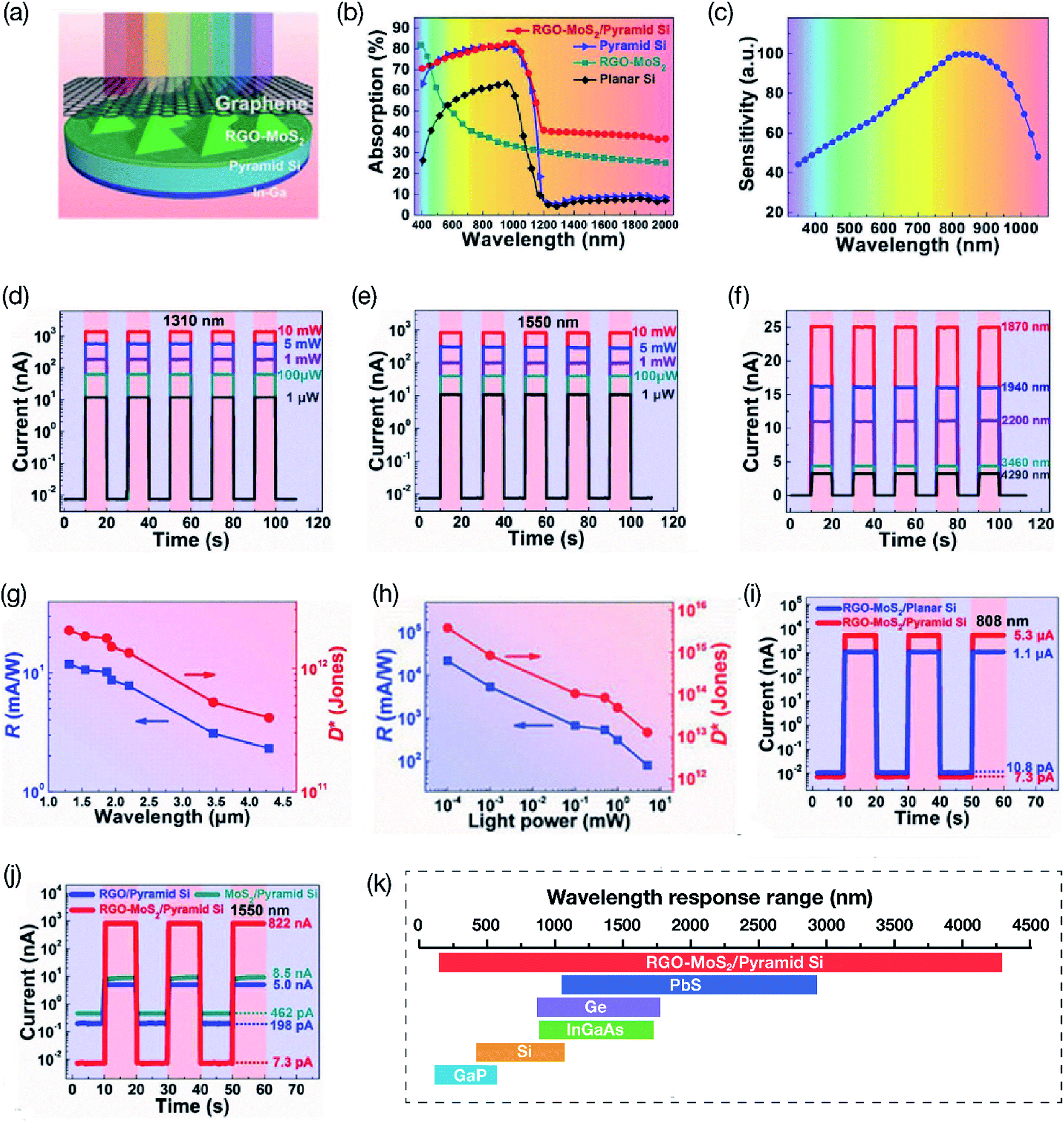 | ||
| Fig. 4 (a) Schematic illustration of the 3D RGO–MoS2/pyramid Si heterojunction-based photodetector. (b) A comparison of the absorption spectra of planar and pyramid Si, RGO (also referred as rGO), and RGO–MoS2/Si heterojunction devices. (c) Photosensitivity of the RGO–MoS2/pyramid Si heterojunction-based device between 350 to 1100 nm wavelength region. (d and e) Photocurrent switching behavior of heterojunction device measured under light illuminations at 1310 and 1550 nm at zero bias voltage (V = 0), self-powered devices. (f) Photocurrent switching behavior of heterojunction devices measured under 1870, 1940, 2200, 3460 and 4290 nm (NIR–MIR) light illuminations. (g) Photoresponsivity (R) and specific detectivity (D*) curves of the heterojunction device measured as a function of wavelength from 1310 nm to 4290 nm at a fixed laser power intensity of 50 mW under zero bias voltage. (h) R and D* curves of the heterojunction photodetector measured as a function of laser power intensity at 808 nm at the 100 nW laser power under zero bias voltage. (i) A comparison of the photocurrent switching behavior of RGO–MoS2/pyramid Si and RGO–MoS2/planar Si heterojunction devices measured at 808 nm wavelength under 1 μW laser power intensity. (j) A comparison of the photocurrent switching behavior of RGO–MoS2/pyramid Si heterojunction device with RGO/pyramid Si and MoS2/pyramid Si devices measured at 1550 nm wavelength under 10 mW laser power intensity. (k) A comparison of the wavelength coverage by the RGO–MoS2/pyramid Si heterojunction-based photodetector along with other traditional semiconductor-based photodetectors. The RGO–MoS2/pyramid Si hybrid heterojunction-based photodetectors operated from 350 nm to 4.3 μm (UV to MIR) ultra-broadband spectral range due to the bandgap narrowing caused by the S vacancy defects in MoS2 crystals. Reprinted with permission from ref. 178, copyright © Wiley. | ||
Another common technique of improving the performance of MoS2 photodetectors is via chemical doping. For example, Kang et al.180 demonstrated that the field-effect mobility increased from 28.75 cm2 V−1 s−1 to 142.2 cm2 V−1 s−1 and the photoresponsivity increased from 219 A W−1 to 5.75 × 10³ A W−1 for APTES/MoS2 hybrid phototransistors after aminopropyltriethoxysilane (APTES) doping of monolayer MoS2. The 24.5-fold increase in the photoresponsivity of the APTES/MoS2 photodetector resulted from the enhanced photocurrent after APTES doping. The photoresponsivity of APTES/MoS2 devices reached 1212.8 A W−1 at a gate bias voltage of Vg = 0 and a Vds of 5 V for a 520 nm wavelength under an incident power of 5.8 mW cm−2. Yu et al.181 used mechanically exfoliated monolayer MoS2 nanosheets sensitized with rhodamine 6G (R6G) organic dye to develop a photodetector with an enhanced photoresponse. The dye-sensitized MoS2/R6G-based photodetector showed a photoresponsivity of 1.17 A W−1, a detectivity of 1.5 × 10⁷ Jones, an EQE of 280% at 520 nm under an incident power of 1 μW and a photoresponse between wavelengths of 405 and 980 nm arising from charge transfer from the rhodamine 6G dye to monolayer MoS2. In addition to photosensitive dyes, the high-κ Al2O3 dielectric has been used for enhancing the photoresponse of MoS2 photodetectors. Huang et al.182 used zinc phthalocyanine (ZnPc) organic dye on the surface of monolayer MoS2 to create a charge transfer interface. Dark and photocurrent of the dye-sensitized ZnPc-treated MoS2 photodetectors increased by 103 to 105 times after a 30 nm thick top Al2O3 passivation layer was used. The photoresponsivity of 281 and 1.74 A W−1 were recorded for the bare MoS2 and ZnPc-treated MoS2 devices at 532 nm under light intensity of 0.07 mW cm−2, respectively. The photoresponse of the Al2O3-passivated MoS2/ZnPc hybrid photodetector was significantly improved: the photoresponsivity increased from 430 A W−1 to 1.4 × 10⁴ A W−1 as the light intensity changed from 3.64 mW cm−2 to 0.07 mW cm−2 under a gate bias of 40 V, respectively. The photoresponse of the MoS2/ZnPc hybrid device was 100 times faster than that of a pristine MoS2 device. Wu et al.183 demonstrated a photoresponsivity of 2.7 × 10⁴ A W−1 for a MoS2 photodetector using an Al2O3/ITO/SiO2 substrate, which increased the light absorption of MoS2 thin films. The high-κ Al2O3 dielectric also yielded a current Ion/Ioff ratio of 109 under a 2 V gate bias voltage, a mobility of 84 cm2 V−1 s−1 and a subthreshold swing of 104 mV dec−1.
Several different strategies including MoS2 plasmonic heterostructures, chemical doping of MoS2 layers, halide perovskites, 2D–0D MoS2/QDs heterostructures, and 2D–2D MoS2/vdWHs hybrid heterostructures have been employed for boosting the light absorption efficiency of MoS2 thin films, hence improving the performance of MoS2 photodetectors. The strategies assist in terms of increasing the carrier mobility and the absorption of incident sunlight by MoS2 hybrid heterostructures.
3.1 MoS2 plasmonic heterostructures
The plasmonic nanostructures have been used for enhancing the optical absorption of semiconductor-based photodetectors. The photoresponse of atomic layered MoS2 photodetectors has been optimized by forming hybrid plasmonic heterostructures for light-harvesting. The gold nanoparticles (AuNPs)@MoS2 heterostructure-based plasmonic photodetectors having AuNPs core and ML MoS2 shell showed 10-fold increase in photoresponsivity (0.5 A W−1) compared with pristine MoS2 phototransistors (0.057 A W−1).163 The maximum photoresponsivity of 30 A W−1 was achieved for the Si-supported AuNPs@MoS2 heterojunction-based gateless photodetector greater than that of Si/MoS2 heterojunction (1.1 A W−1) phototransistors. Bang et al.184 developed a monolayer (1L) MoS2 photodetector exploiting the surface plasmon of a one-dimensional (1D) silver nanowire (AgNW) network. Fig. 5(a–d) shows the schematic diagram of the 1L-MoS2/AgNW-based photodetector, dark field image of a hybrid photodetector, and photocurrent–voltage curves of pristine 1L-MoS2 and the 1L-MoS2/AgNWs hybrid photodetectors as a function of applied voltage (from −5 V to +5 V) and the time-dependent photocurrents. The current Ion/Ioff ratios of 1.39 × 10⁴ and 62.97 were measured for the 1L MoS2/AgNW hybrid and pristine 1L-MoS2 photodetectors, respectively. The 1L MoS2/AgNW hybrid heterostructure-based device showed 560- and 250-fold increases in the PL and photocurrent, respectively, compared with the pristine 1L MoS2 device. Similarly, the photoresponsivity of 59.60 A W−1 and detectivity of 4.51 × 10¹⁰ Jones for the 1L MoS2/AgNW hybrid photodetector were 1000 times enhanced compared to those of the pristine 1L-MoS2 photodetector (0.05 A W−1 and 4.11 × 10⁷ Jones). The significant improvement in the optoelectronic properties of the 1L MoS2/AgNW hybrid photodetector occurred due to the surface plasmon coupling of the AgNW network. In another study, Jing et al.185 enhanced the localized surface plasmon resonance (LSPR) by depositing Ag nanoparticles onto monolayer MoS2 for developing phototransistors. AgNPs/MoS2 hybrid-based phototransistors showed a 470% increase in photoresponsivity, changing from 5.35 × 10³ A W−1 to 2.97 × 10⁴ A W−1 at 610 nm for 25 nm AgNPs. The interactions between MoS2 layers and light are enhanced by the integrated Au or Ag nanostructures due to the LSPR, which significantly improves the photoresponse of plasmon heterostructure-based hybrid MoS2 photodetectors. Sun et al.186 used silica layer-coated silver nanocubes (AgNCs) with optimized LSP in the gap mode for developing a flexible MoS2 photodetector. The PL spectrum of MoS2/Ag nanocubes hybrid was found to be significantly enhanced compared with MoS2 film after modifying of Ag NCs with underneath Ag thin film due to interactions between the MoS2 excitons and LSP in the gap mode. Fig. 5(e–g) compare the photoresponsivity and photocurrent of MoS2 and flexible MoS2/Ag nanocubes (NCs) hybrid-based photodetectors as a function of incident laser power and time, respectively. Photocurrent rise (τrise) and decay (τdecay) times and mechanical stability of flexible MoS2/AgNCs hybrid-based photodetector are also depicted. The photocurrents of the photodetectors fabricated using pristine MoS2 film and MoS2 film with underneath Ag film were almost the same (48–50 nA) at 3 V under 520 nm laser illumination with 46 nW incident power whereas the photocurrent of flexible photodetector having MoS2 film in the gap of Ag layer and AgNCs was considerably increased to 0.91 μA under similar experimental conditions due to the Ag nanocubes. The AgNCs decorated MoS2 film shows 19-fold increment in photocurrent compared with pristine MoS2 film. The photoresponsivity of MoS2 with AgNCs based flexible photodetector increased 38 times to 7940 A W−1 at 3 V under 2.2 pW incident power compared with pristine MoS2 film with decreasing incident power intensity due to the reduced scattering and recombination of the photogenerated charge carriers. Photocurrent rise time (τrise) of 0.3 s and decay time (τdecay) of 1.6 s were estimated for the flexible MoS2/AgNCs hybrid-based photodetector. The flexible photodetector showed good mechanical stability after bending at a curvature of 8 mm for 10000 times because 71% photocurrent ratio of devices was retained. The photocurrent initially decreased up to 3000 bending cycles, but no noticeable decrease in photocurrent ratio was observed thereafter. These studies show that the integration of plasmonic nanostructures with MoS2 atomic layers can significantly increase the photoresponsivity of MoS2 based photodetectors.
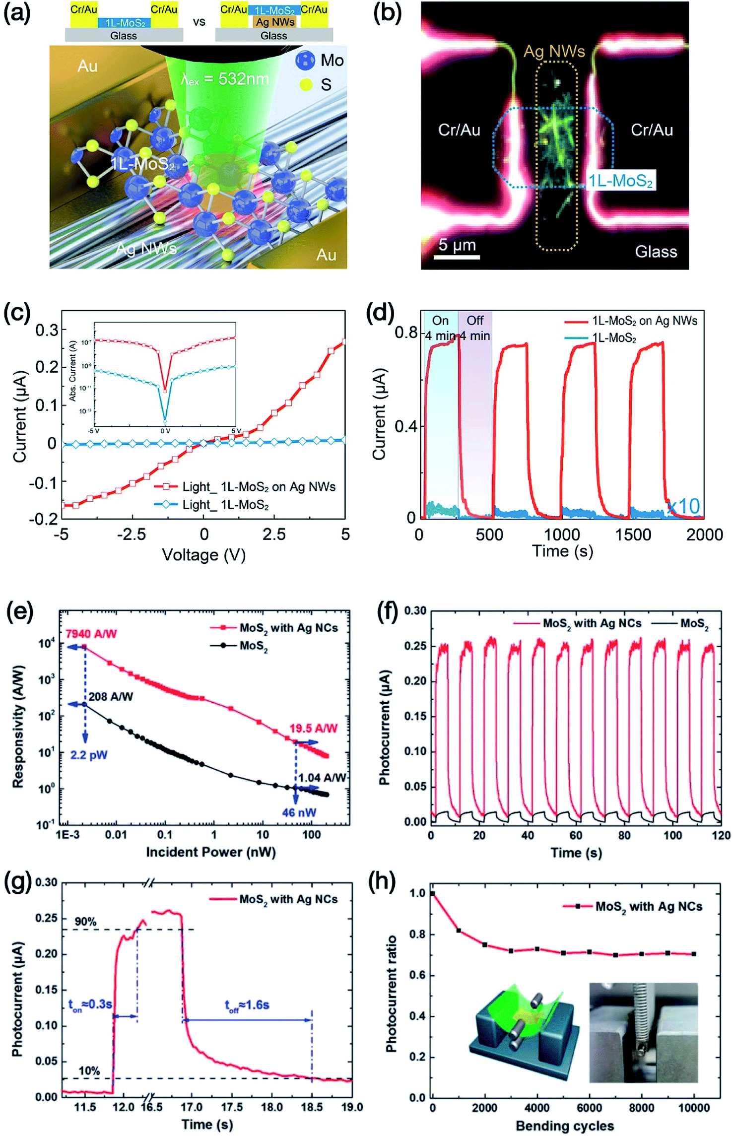 | ||
| Fig. 5 (a) Schematic diagram of the 1L-MoS2 and Ag nanowires (NWs) based photodetector. Upper area shows the schematic diagrams of the pristine 1L-MoS2 and the 1L-MoS2/AgNWs hybrid photodetector on a glass substrate along with Cr/Au electrodes. (b) Dark field image of the 1L-MoS2/AgNWs hybrid photodetector (60% density of AgNWs). (c) A comparison of the photocurrent–voltage curves between pristine 1L-MoS2 (blue line) and the 1L-MoS2/AgNWs hybrid photodetector (red line) measured at 532 nm. The inset represents a logarithmic scale of the photocurrent–voltage characteristic. (d) Time dependent photocurrent of the pristine 1L-MoS2 (blue) and 1L-MoS2/AgNWs hybrid photodetectors (red) recorded with an Ion/Ioff time of 4 min. Reprinted with permission from ref. 184, copyright © American Chemical Society. (e) Photoresponsivity of MoS2 and MoS2/Ag nanocubes (NCs) hybrid-based photodetectors as a function of incident laser power. (f) A comparison of the transient photocurrent of MoS2 and MoS2/Ag nanocubes (NCs) photodetectors under periodical Ion/Ioff illumination at 1 V. (g) Photocurrent rise (ton) and decay (toff) times of MoS2/Ag NCs hybrid-based photodetector. (h) Photocurrent of MoS2/Ag NCs hybrid-based photodetector as a function of number of bending cycles, where the insets show schematic and photograph of a bending setup. Reprinted with permission from ref. 186, copyright @ Wiley. | ||
3.2 Chemical doping of MoS2 layers
As discussed above, performance of MoS2 photodetectors can be significantly increased by doping MoS2 layers with APTES,180 rhodamine 6G181 and ZnPc182 organic dyes, which efficiently generate charge transfer interfaces between MoS2 and chemical dopants. A few examples of boosting the performance of MoS2 photodetectors via chemical doping are presented here. Heo et al.187 used n-type doping of MoS2 flakes with triphenylphosphine (PPh3) to improve the electronic and optoelectronic properties of multilayer MoS2 by utilizing charge transfer from PPh3 to MoS2, in which the PPh3 doping concentration ranged from 1.56 × 10¹¹ to 9.75 × 1012 cm−2. The PPh3 doping considerably increased the mobility from 12.1 to 241 cm2 V−1 s−1 and the Ion/Ioff current ratio from 8.72 × 10⁴ to 8.70 × 10⁵ for the MoS2 transistor. The photoresponsivity of the MoS2 photodetector similarly increased from 2.77 × 10³ to a maximum value of 3.92 × 10⁵ A W−1 under an applied laser power of 5 pW. The detectivity decreased by three orders of magnitude, from 6.82 × 10¹³ Jones to 2.36 × 10¹⁰ Jones, as the device doping temperature was increased from 150 °C to 350 °C. The MoS2 photodetector also showed long-term stability, where the photoresponsivity decreased by 1.58% after 14 days of exposure to air; additionally, the PPh3 doping was reversible, allowing repetitive use of the photodetector device. For example, a MoS2/Si heterojunction-based photodetector showed no degradation in the photovoltage after storing in an air atmosphere over a period of a month.162The chemical doping of monolayer MoS2 film over a 13 cm2 area for developing photodetector devices was reported by Kim et al.161 The n-type MoS2 semiconductor transitions into the p-type semiconductor after doping with Nb. Raman spectroscopy, X-ray photoelectron spectroscopy (XPS), and photoluminescence (PL) spectroscopy were used to characterize the doped MoS2. The Nb-doped MoS2 showed binding energy peaks at lower values compared with MoS2. The Nb- and Mn-doped monolayer MoS2 FETs showed p-type and n-type doped MoS2 characteristics, respectively. Fig. 6 shows doped MoS2 photodetectors, transfer curves (drain current versus gate voltage) and photoresponsivity of Nb-doped MoS2 photodetectors as a function of optical power and compares the photoresponsivity, EQE, and detectivity of Nb-doped MoS2 photodetectors with updoped MoS2 photodetectors at different laser wavelengths. A sublinear relationship (R ∝ Pα) was observed for Nb-doped MoS2 photodetector between photoresponsivity (R) and optical power (P), which yielded an α value of −0.9 using the power function fitting method. The Nb-doped MoS2 photodetector showed photoresponsivity of 2 × 10⁵ A W−1, which is 106 times higher compared with the photoresponsivity of 0.52 A W−1 for the MoS2 film measured under similar conditions at a 550 nm laser wavelength. The highest photoresponsivity of 4.83 × 10⁵ A W−1 was recorded at 750 nm wavelength for the Nb-doped MoS2 photodetector. Likely, the EQE for Nb-doped MoS2 photodetector was found to be 9.31 × 10⁷%, which was 106 times higher compared with EQE of 107% for the MoS2 device at 450 nm wavelength. The Nb-doped MoS2 photodetector showed detectivity of 5.0 × 10¹² Jones, compared with the detectivity of 3.93 × 10⁸ Jones for the updoped MoS2 photodetector at 750 nm wavelength, which resulted in 105 times higher detectivity after Nb-doping. The photocurrent values of Nb-doped MoS2 devices were also increased by 105 folds due to the charge-transfer process. The Nb-doped MoS2 devices also exhibited faster rise/decay times of 4.9 ms and 5.7 ms compared with 0.63 s and 1.63 s for the updoped MoS2 devices at 550 nm laser wavelength, respectively. The Nb-doped MoS2 photodetector devices showed stability for 30 days under ambient conditions.
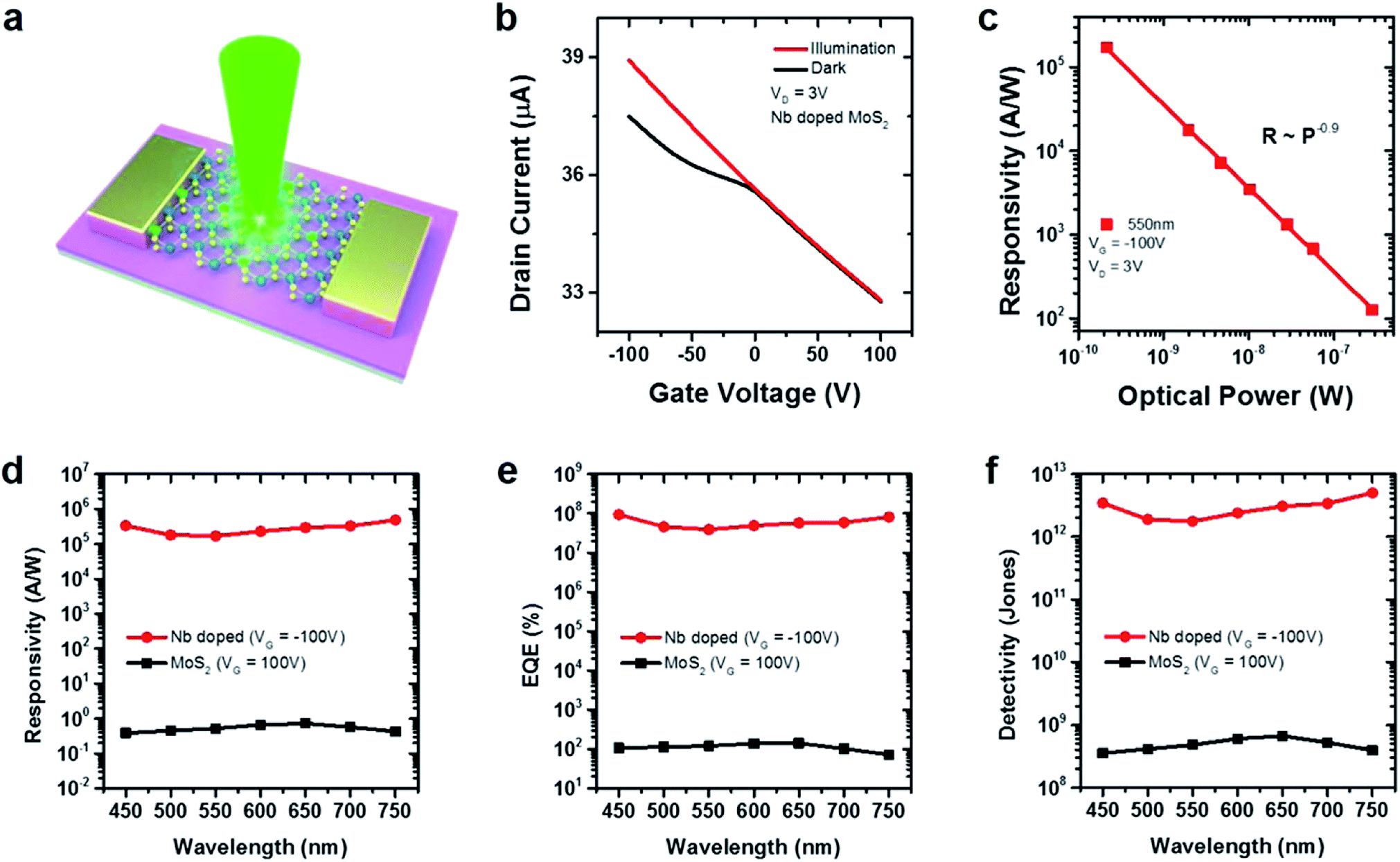 | ||
| Fig. 6 (a) Schematic illustration of doped MoS2 photodetectors. (b) Transfer curves of Nb-doped MoS2 photodetectors at 550 nm laser wavelength under 282 nW optical power. (c) Photoresponsivity (R) of Nb-doped MoS2 photodetectors as a function of optical power (P) at 550 nm laser wavelength and at Vd = 3 V and Vg = −100 V. A comparison of photoresponse characteristics of Nb-doped MoS2 photodetectors with updoped MoS2 photodetectors. (d) Photoresponsivity, (e) EQE, and (f) detectivity of Nb-doped MoS2 photodetectors and updoped MoS2 photodetectors at Vg = −100 V as a function of laser wavelength. Reprinted with permission from ref. 161, copyright © American Chemical Society. | ||
The phototransistors utilizing hybrid MoS2/PbS QDs, were fabricated by Pak et al.188 in which the PbS QDs were surface modified with n-type tetrabutylammonium iodide (TBAI) and p-type 1,2-ethanedithiol (EDT) ligands to develop p–n junctions. The MoS2/PbS-TBAI/PbS-EDT hybrid device showed a photoresponsivity of 5700 ± 71.2 A W−1 for a single-junction device and 6120 ± 96.9 A W−1 for a double-junction device at an incident laser power of 20 pW. The photocurrent rise time of 40 ms for the single-junction device was reduced to 950 μs for the double-junction device. The efficient charge transfer occurring in the MoS2/PbS QD hybrid photodetector yielded a maximum photoresponsivity of 5.4 × 10⁴ A W−1 and a detectivity of 1 × 10¹¹ Jones. High photoresponsivity of 2570 A W−1 and detectivity of 2.2 × 10¹² Jones at 635 nm in a few-layer MoS2 photodetector have been demonstrated under zero gate voltage with the use of a poly(vinylidene fluoride-trifluoroethylene) [P(VDF-TrFE)] ferroelectric polymer gate.137 This MoS2/P(VDF-TrFE) hybrid photodetector also showed photodetection over the 0.85 μm to 1.55 μm spectral region and excellent stability over 90000 repeated cycles of operation.
Organic molecules and polymers have been hybridized with MoS2 to develop photodetectors. Sun et al.189 used narrow bandgap organic semiconducting polymer, poly(diketopyrrolopyrrole-terthiophene) (PDPP3T), into large bandgap monolayer MoS2 to develop UV-NIR photodetectors. The photoresponsivities of MoS2/PDPP3T based phototransistors were enhanced by one to two orders of magnitude compared with MoS2. Flexible MoS2/PDPP3T photodetectors that were fabricated on a PET substrate. The MoS2/PDPP3T hybrid showed photoresponsivities of 276, 445, and 269 mA W−1 and detectivity values of 2.59 × 10⁸, 3.14 × 10⁸, and 2.53 × 10⁸ Jones at 365, 660, and 850 nm, respectively. The flexible MoS2/PDPP3T photodetectors were developed on a PET substrate which exhibited photoresponse from 365 nm to 940 nm. The bending testing of flexible MoS2/PDPP3T photodetector was conducted under 660 nm light illumination a 9 mm bending radius where some decrease in the photocurrent was noticed after 10000 bending cycles. Likely, the environmental stability of the flexible MoS2/PDPP3T photodetector was also evaluated without any encapsulation in an air atmosphere for 35 days where slight changes were observed both in the dark and photo currents. MoS2/PDPP3T hybrid photodetector devices demonstrated both mechanical stability and durability in the air.
3.3 Halide perovskite MoS2 heterostructures
Organometallic halide perovskites have emerged as an important class of light harvesting materials for developing solar cells8,9,130,131 because of their tunable bandgap, extended light absorption over a broad spectral range, high photoconversion efficiencies, charge-carrier mobilities, and ease of solution processing into ultrathin layers. These unique optoelectronic properties of perovskites have been utilized in improving the performance of MoS2 photodetectors. Wu et al.190 developed hybrid phototransistors using 0D cesium lead halides perovskite (CsPbI3−xBrx) QDs and 2D monolayer MoS2. The CsPbI3−xBrx QD/1L MoS2 0D–2D mixed-dimensional vdW heterostructure-based photodetectors showed a high photoresponsivity of 7.7 × 10⁴ A W−1, a detectivity of 5.6 × 10¹¹ Jones, and an EQE value greater than 107% at 532 nm light illumination under optical power of 1.5 μW due to the photogating effect. Also under similar illumination conditions, the photocurrent of CsPbI3−xBrx QDs/1L MoS2 hybrid phototransistor was found to be increased by 15.3 times that of a pristine MoS2 phototransistor, indicating the efficient separation of photogenerated carriers and the strong absorption of 0D CsPbI3−xBrx QDs.MoS2 layers combined with perovskite CsPbBr3 nanosheets have been investigated for fabricating photodetectors, as reported by Song et al.191 The MoS2/CsPbBr3 hybrid-based photodetector showed a photoresponsivity of 4.4 A W−1, a detectivity of 2.5 × 10¹⁰ Jones, and a 302% EQE arising from photoexcited carrier separation at the interface of the perovskite CsPbBr3 nanosheet and MoS2 layer. The photoresponsivity of the MoS2/CsPbBr3 hybrid-based photodetector increased by three orders of magnitude compared to the MoS2 photodetector without the perovskite CsPbBr3. The response time of the hybrid photodetector decreased from 65.2 to 0.72 ms after adding MoS2 layers. The high photon absorption by the CsPbBr3 perovskite layer and the carrier transport by the MoS2 layer contributed to the high performance of the photodetector devices. The 3 MoS2/CsPbBr3 hybrid, CsPbBr3 and MoS2 photodetector devices showed current in the 0.1–1 nA range. Photocurrents of 5030, 1230, and 54 nA were measured for the MoS2/CsPbBr3 hybrid, CsPbBr3, and MoS2, respectively. Light on/off ratios of 16700, 14300, and 150 were calculated for the MoS2/CsPbBr3 hybrid, CsPbBr3, and MoS2 photodetector devices, respectively. PL quenching, as well as a fast decay time, was observed for the MoS2/CsPbBr3 hybrid due to the charge transfer from the perovskite CsPbBr3 nanosheet to the MoS2 atomic layers. Kang et al.192 reported perovskite/MoS2/APTES hybrid heterostructure-based photodetector devices. The photoresponsivity of a MoS2 photodetector was enhanced from 636 to 4.9 × 10³ A W−1 and detectivity from 1.53 × 10⁹ to 8.76 × 10¹⁰ Jones for a perovskite/MoS2 hybrid device after applying the perovskite layer at 520 nm. The similar increment was also observed for 655 and 785 nm laser wavelengths, but for 850 nm. The photocurrent of the perovskite/MoS2/APTES hybrid photodetector was increased by 25.9 times that of the MoS2 photodetector at 520 nm wavelength. The photoresponsivity and detectivity of the perovskite/MoS2/APTES hybrid photodetector device were enhanced from 816.6 to 2.11 × 10⁴ A W−1 and from 3.93 × 10⁹ to 1.38 × 10¹⁰ Jones after APTES n-doping, respectively. The photoresponsivity of the perovskite/MoS2/APTES hybrid photodetector was increased by 94.2 times, from 2.11 × 10⁴ to 1.94 × 10⁶ A W−1 at 520 nm as a function of incident laser power (1.57 nW to 4.63 pW), while the highest detectivity value was 1.29 × 10¹² Jones due to the decreased scattering between photogenerated electrons. The perovskite/MoS2/APTES hybrid photodetectors showed significantly higher photoresponsivity values compared with the MoS2/APTES photodetector.180 The performance of photodetector devices followed the sequence as: perovskite/MoS2/APTES > perovskite/MoS2 > MoS2, as clearly evident from the above-mentioned results. Since perovskites are susceptible to environmental degradation,8,130 therefore, the stability of perovskite/MoS2/APTES photodetectors was improved by applying encapsulating layers of octadecyltrichlorosilane (OTS) and PMMA. The stability of non-encapsulated, PMMA and OTS/PMMA encapsulated perovskite/MoS2/APTES photodetector devices in air was measured at different wavelengths: 520, 655, 785 and 850 nm. Photoresponsivity and detectivity deteriorated by 50% and 70% after 68 h for PMMA and 20.4% and 28.7% after 200 h for OTS/PMMA encapsulated devices, and 20.4–24.8% and 28.7–34.2% for perovskite/MoS2/APTES photodetectors at different wavelengths, respectively. These data showed that performance of MoS2 photodetectors can be improved by applying a perovskite absorption layer and furthermore via a chemical doping process.
The flexible perovskite/MoS2 hybrid photodetectors were developed using a polyethylene terephthalate (PET) substrate. Sun et al.76 used CVD grown atomic layered MoS2 film, deposited a 20 nm Ti/50 nm Au thick electrode and then spin-coated a triple cations [Cs0.05(MA0.17FA0.83)0.95Pb(I0.83Br0.17)]3 lead mixed-halide perovskite layer to fabricate a hybrid photodetector. Fig. 7 shows the schematics and energy-band diagram of the perovskite/MoS2 hybrid photodetector under illumination, photoresponse of the pristine MoS2 and perovskite/MoS2 hybrid photodetector devices and mechanical stability test of the flexible hybrid photodetector device up to 20000 bending cycles. The flexible perovskite/MoS2 hybrid photodetectors showed photoresponsivity of 342 A W−1 at 2 V bias potential without any gate voltage at 520 nm under 2.2 pW incident power. The hybrid photodetector devices showed high stability without any encapsulation, photoresponse and decay times of 27 ms and 21 ms, respectively. The hybrid devices were fabricated on rigid SiO2/Si, glass and flexible PET substrates. The pristine MoS2 photodetector device showed the photocurrent of 32 nA at 2 V bias potential with 20 nW incident power, which increased to 84 nA after spin-coating the perovskite layer. The perovskite/MoS2 hybrid device showed photocurrent of 2 pA at 1 V and 3.8 pA at 2 bias potential. At 1 V bias potential, the photocurrent of the hybrid device increased from 2 pA in the dark to 40 nA under illumination. The hybrid photodetector device having 10 μm channel exhibited the highest photoresponsivity value of 1.7 A W−1 under 50 nW incident power. The estimated detectivity was 1.14 × 10¹² Jones. The photocurrent of the hybrid devices increased as a function of increased incident power. The photoresponsivity of the hybrid photodetector device was dramatically increased to 342 A W−1 as the incident power decreased to 2.2 pW because of the suppressed scattering between the photogenerated charge carriers, and mechanical stability test on flexible perovskite/MoS2 hybrid photodetectors was performed with 5 mm curvature up to 20000 bending cycles. The device retained 91% photocurrent value under bending compared with the corresponding I–V curves of a device without bending. There was no noticeable decline in photocurrent ratio from 2000 to 20000 bending cycles, indicating the strong mechanical stability of the flexible perovskite/MoS2 hybrid devices.
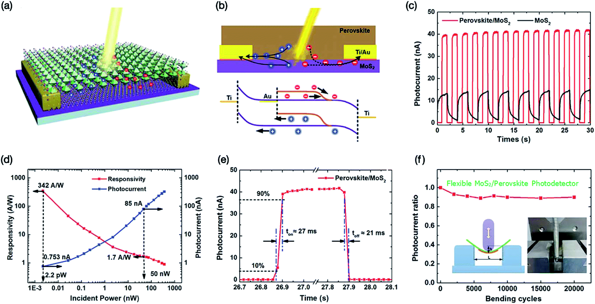 | ||
| Fig. 7 (a) Schematic illustration of perovskite/MoS2 hybrid based photodetector. (b) Working mechanism and energy-band diagram of flexible perovskite/MoS2 hybrid photodetector under illumination. (c) A comparison of the transient photoresponse of the pristine MoS2 and flexible perovskite/MoS2 hybrid based photodetectors under on/off illumination. (d) Photoresponsivity and photocurrent of the flexible perovskite/MoS2 hybrid photodetector devices as a function of laser incident power. (e) Photoresponse rise and decay time of the flexible perovskite/MoS2 hybrid based photodetector. (f) Mechanical stability test of the flexible perovskite/MoS2 hybrid photodetector device up to 20000 bending cycles. Reprinted with permission from ref. 76, copyright @ Elsevier. | ||
3.4 2D–0D MoS2–quantum dots (QDs) heterostructures
As discussed above, photodetectors fabricated with hybrid MoS2/PbS QDs yield significantly high photoresponsivity.188 0D QDs have been used for improving the performance of MoS2 photodetectors. Huo et al.193 developed photodetectors by incorporating mercury telluride (HgTe) colloidal QD film into a TiO2-encapsulated few-layer MoS2 channel. In the MoS2/TiO2/HgTe hybrid heterostructure, TiO2 is a buffer layer between the MoS2 channel and the HgTe QD layer that acts as an electron accepting medium to form a p–n junction with the HgTe QDs to facilitate the transfer of photogenerated charges from the HgTe QDs to the MoS2 channel. MoS2/TiO2/HgTe hybrid photodetectors showed a high photoresponsivity of 106 A W−1 under an incident power of 70 fW (0.35 μW cm−2) at a gate voltage (Vg) of −15 V and a Vds of 1 V, which is seven orders of magnitude higher than that of the HgTe QD photodetector due to the low carrier mobility (2 × 10⁻³ cm2 V−1 s−1) of the HgTe QDs. The detectivity of MoS2/TiO2/HgTe hybrid photodetectors was 1 × 10¹² Jones at a 2.0 μm wavelength, which is four orders of magnitude higher than that of pure HgTe-based photodetectors (107 to 108 Jones). This study is an excellent example of extending the spectral wavelengths of a MoS2-based photodetector over 2.0 μm. In another study, Zhang et al.194 reported 2D MoS2–0D zinc cadmium selenide (ZnCdSe)/zinc sulfide (ZnS) colloidal QD-based photodetectors, where monolayer (1L) to multilayer (ML) MoS2 thin film acts as a carrier transport channel and a core/shell ZnCdSe/ZnS QDs sensitizing thin layer functions as a light harvester. Fig. 8 compared the photoresponsivity and detectivity as a function of laser incident power for the pristine MoS2 based photodetctors with hybrid MoS2–ZnCdSe/ZnS QD-based photodetectors having monolayer MoS2 (1L), bilayer MoS2 (2L), trilayer MoS2 (3L), and multilayer MoS2 (ML). There is a very significant increase in photocurrent, photoresponsivity, and detectivity after adding ZnCdSe/ZnS QD sensitizing layer. The photocurrent of hybrid MoS2–ZnCdSe/ZnS QD-based photodetectors increased by 1000 folds compared with pristine MoS2 photodetectors. The response time of the MoS2–ZnCdSe/ZnS QD-based photodetector was reduced to 0.3 s from 15 s for MoS2 layers, making the hybrid device 50 times faster. The schematic of the MoS2–ZnCdSe/ZnS QD interface and their energy diagram depict the transfer of electrons from ZnCdSe/ZnS QDs to MoS2 layers via a tunneling process and the transfer of excitons from ZnCdSe/ZnS QDs to the MoS2 layer via nonradiative energy transfer (NRET) processes after a heterojunction formation. In the NERT process, the MoS2 layer acts as an acceptor, whereas the ZnCdSe/ZnS QDs thin layer acts as a donor. The photoresponsivity of the hybrid MoS2–ZnCdSe/ZnS QD-based photodetectors increased by three orders of magnitude to 3.7 × 10⁴ A W−1 compared to pristine MoS2 layers of 10 A W−1. Likely, the detectivity of the MoS2–ZnCdSe/ZnS QD-based photodetector increased to 1.0 × 10¹² Jones, and the gain increased by five orders of magnitude to 1.08 × 10⁵ after adding a layer of QDs due to the increased absorption and efficient transfer of energy from the photoexcited ZnCdSe/ZnS QDs layer to MoS2 layers. The better performance of the 2D–0D hybrid photodetector is associated with high carrier mobility in the MoS2 layer and the creation of effective photon absorption/exciton in the ZnCdSe/ZnS QDs layer. The MoS2 layers efficiently quench the fluorescence of the ZnCdSe/ZnS QDs in the 2D–0D hybrid nanostructures exhibiting ultrasensitivity and high gain.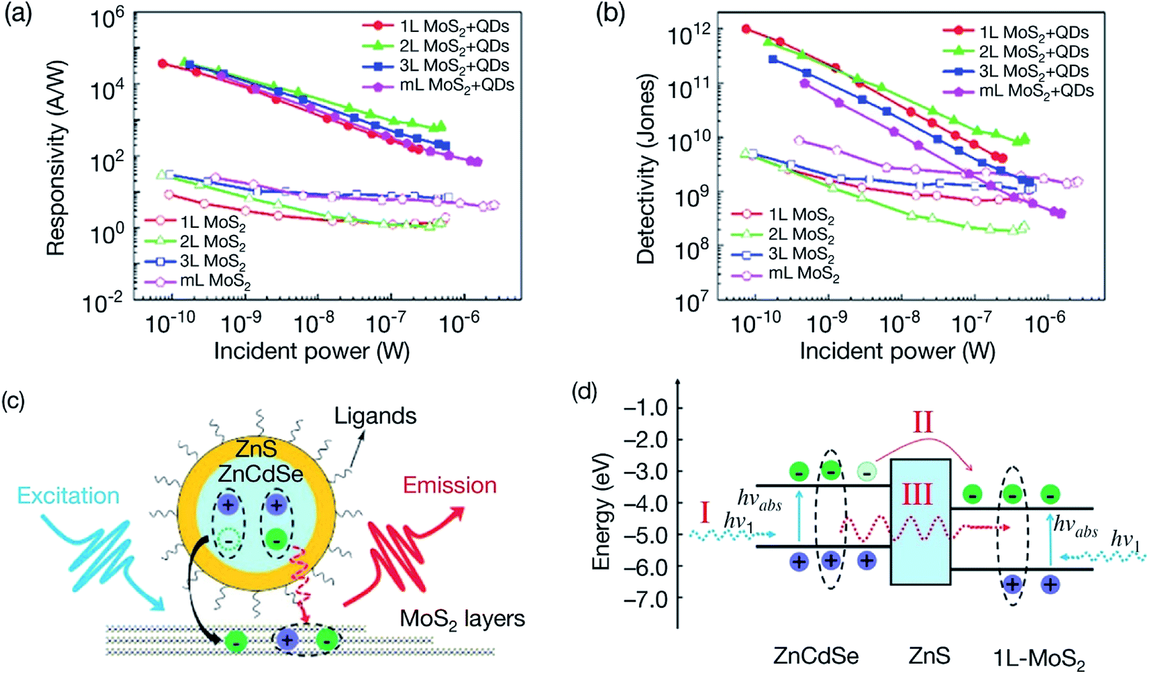 | ||
| Fig. 8 (a and b) A comparison of photoresponsivity and detectivity of pristine MoS2 based photodetctors with hybrid MoS2–ZnCdSe/ZnS QD-based photodetectors having different MoS2 layers; monolayer MoS2 (1L), bilayer MoS2 (2L), trilayer MoS2 (3L), and multilayer MoS2 (ML) as a function of laser incident power. Both responsivity and detectivity increased significantly after adding QD sensitizing layer. (c) Schematic of the MoS2–ZnCdSe/ZnS QD interface showing the transfer of electrons from ZnCdSe/ZnS QDs to MoS2 layers via a tunneling process (represented by black arrow) and the transfer of excitons from ZnCdSe/ZnS QDs to MoS2 layer via nonradiative energy transfer (NRET) processes (represented by red dashed arrow) under an illumination. (d) Energy diagram of the 1L MoS2–ZnCdSe/ZnS QD interface after a heterojunction formation where three photoelectrical processes are involved; (I) photon excitation in 1L-MoS2 and ZnCdSe/ZnS QDs; (II) transfer of electrons from the ZnCdSe/ZnS QDs to 1L-MoS2 via a tunneling process and (III) exciton transfer from the ZnCdSe/ZnS QDs to 1L-MoS2 via NRET processes. Reprinted with permission from ref. 194, copyright © American Chemical Society. | ||
3.5 2D–2D MoS2-2D van der Waals heterostructures (vdWHs)
MoS2-based photodetectors have been designed and developed using different electrode materials and van der Waals heterostructures (vdWHs) to improve their optoelectronic properties. The performance of MoS2-based photodetectors can be increased using rGO layers.178,179 Fig. 9(a–c) shows a schematic of the multilayer MoS2 photodetector developed with Mo bottom contacts (100 nm) on thermally oxidized SiO2/Si substrates (270 nm) and the photoresponsivity and EQE of the ML MoS2 photodetector measured over the 400–1100 nm spectral region, as reported by Saenz et al.195 The photodetector exhibited ultrahigh photoresponsivity of 1.4 × 10⁴ A W−1 and detectivity of 2.3 × 10¹¹ Jones at a 700 nm wavelength with a 14.5 pW laser power for the multilayer MoS2 device fabricated using 100 nm thick Mo bottom electrodes, with a broadband photoresponse from the UV to IR regime. The photoresponsivity increased from 8 × 10³ A W−1 at 400 nm to 1.4 × 10⁴ A W−1 at 1100 nm at a bias voltage of 20 V, and the EQE varied from 3.6 × 10⁴ to 1.4 × 10⁴ within the 400 nm to 1100 nm wavelength range. Photoresponsivities of 1 × 10³ A W−1 and 42 A W−1 were recorded at incident powers of 70 pW and 15.85 nW, respectively, at a bias voltage of 5 V and 300 K. The decrease in the photoresponsivity resulted from the loss of photocarriers due to recombination effects. Vu et al.196 used MoS2/h-BN/graphene vdWHs to develop a photodetector. Fig. 9(d–f) depicts a schematic of the MoS2/h-BN/graphene photodetector, its cross-sectional STEM image, its energy dispersive X-ray spectroscopy (EDS) elemental mapping and its photoresponsivity and absorbance as a function of photon energy. An h-BN insulating layer was inserted between the MoS2 photoabsorber and the graphene electrode. In these vdWHs, the dark carriers are suppressed at the graphene/h-BN barrier (2.7 eV), whereas the tunneling of photocarriers is facilitated at the MoS2/h-BN junction (1.2 eV). Varying the thickness of the h-BN insulating layer from 0–25 nm played an important role in the tunneling of the dark carriers and photocarriers; a 7 nm thick h-BN barrier layer was most effective in blocking the conduction of dark carriers and facilitating the tunneling of photocarriers through the low-hole MoS2/h-BN junction. The photodetector fabricated from MoS2/h-BN/graphene vdWHs with a 7 nm thick h-BN layer exhibited a photoresponsivity of 180 A W−1 with a maximum photocurrent/dark current (Iphoto/Idark) ratio of 105 and a detectivity of 2.6 × 10¹³ Jones. The detectivity of the vdWH-based photodetector was 1000 higher compared with the values of 2.5 × 10¹⁰ Jones for the lateral MoS2 p–n junction170 and 5 × 10¹⁰ Jones for monolayer MoS2-based photodetectors.197 Furthermore, the rise/fall times of 0.23 s/0.25 s for the vdWH-based photodetector were 1000 times faster than those of the monolayer MoS2-based photodetector.171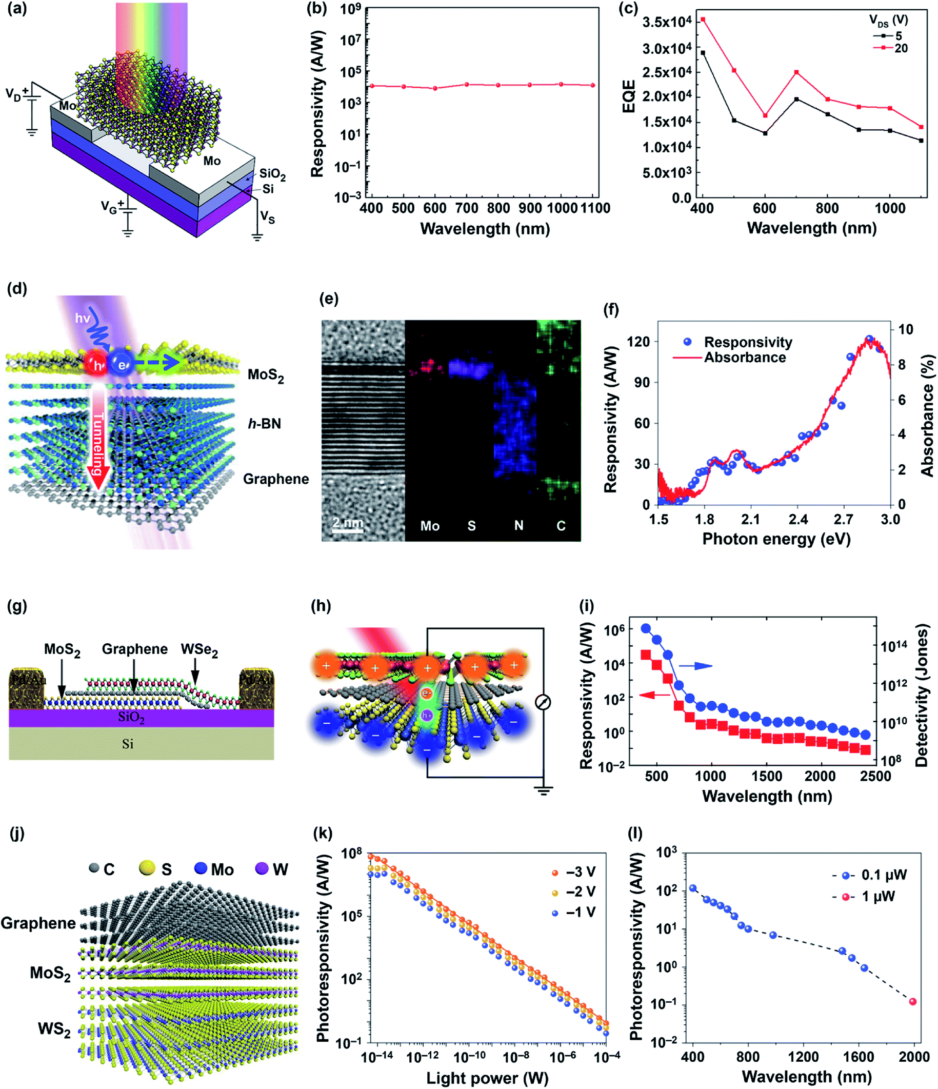 | ||
| Fig. 9 (a) Schematic of the multilayer MoS2 photodetector fabricated using 100 nm thick Mo bottom contacts on 270 nm thick thermally oxidized SiO2/Si substrates. (b) Photoresponsivity and (c) external quantum efficiency (EQE) of the ML MoS2 photodetector as a function of wavelength over the 400–1100 nm spectral region. Reprinted with permission from ref. 195, copyright © 2018 Springer Nature Limited. (d) Schematic of the MoS2/h-BN/graphene vdWH photodetector using the MoS2 layer as a photon absorber, the h-BN layer as a selective hole tunneling layer and the graphene layer as a bottom electrode. The generation of an electron–hole pair upon light illumination and occurrence of selective hole carrier tunneling through the h-BN layer. (e) Cross-sectional STEM image and energy dispersive X-ray spectroscopy (EDS) elemental mapping of the MoS2/h-BN/graphene vdWHs. (f) Photoresponsivity and absorbance of the MoS2/h-BN/graphene photodetector as a function of photon energy. Reprinted with permission from ref. 196, copyright © American Chemical Society. (g) Side view of MoS2/graphene/WSe2 vdWHs. (h) Schematic drawing of atomically layered MoS2/graphene/WSe2 vdWHs for broadband photodetection. (i) Photoresponsivity and detectivity (D*) of the MoS2/graphene/WSe2-based broadband photodetector in the 400 nm to 2400 nm wavelength range. Reprinted with permission from ref. 198, copyright © American Chemical Society. (j) Schematic of the graphene/MoS2/WS2 vdWH-based optical-fiber compatible photodetector. (k) Photoresponsivity of the graphene/MoS2/WS2-based broadband optical-fiber compatible photodetector as a function of laser illumination power at different bias voltages. (l) Photoresponsivity of the graphene/MoS2/WS2-based broadband optical-fiber compatible photodetector as a function of wavelength in the 400 nm to 2000 nm spectral range. Reprinted with permission from ref. 199, copyright © Wiley. | ||
Similarly, atomically thin layered MoS2/graphene/WSe2 (p–g–n) vdWHs were developed by Long et al.198 In this vdWH, graphene was sandwiched within the p–n junction to broaden the absorption spectral range and photodetection sensitivity. Fig. 9(g–i) shows a side view of MoS2/graphene/WSe2 vdWHs, a schematic for the broadband photodetection and the wavelength-dependent photoresponsivity and detectivity (D) of the MoS2/graphene/WSe2-based broadband photodetector over the 400 nm to 2400 nm wavelength range. Both the photoresponsivity and detectivity decreased with increasing excitation laser wavelength. The maximum photoresponsivity and detectivity values of the p–g–n heterostructure-based photodetector were on the order of 104 A W−1 and 1015 Jones in the visible range and decreased to a few mA W−1 and 109 Jones at the 2400 nm wavelength, respectively. A photoresponsivity of 4250 A W−1, a detectivity of 2.2 × 10¹² Jones and an EQE value of 1.0 × 10⁶% were measured at 532 nm with a 0.2 nW laser power intensity for the p–g–n heterostructure-based photodetector, while the photoresponsivity dropped to 306 mA W−1 in the near-IR region, 940 nm with a 17 nW laser power. The photocurrent mapping conducted at 830 nm with a 20.5 μW laser power indicated that the overlapping regions of the MoS2, graphene and WSe2 atomic layers are responsible for the strong photoresponse instead of the electrode regions. The MoS2/graphene/WSe2 heterostructure-based broadband photodetector also showed a fast photoresponse with a 53.6 μs rise time and a 30.3 μs fall time, and can be used from the visible to near-IR spectral range at room temperature.
Fig. 9(j–l) illustrates a schematic of the graphene/MoS2/WS2 vdWH-based optical-fiber compatible photodetector fabricated by Xiong et al.199 The photoresponsivity of this optical-fiber tuned photodetector was recorded as a function of applied laser power at different bias voltages and in the 400 nm to 2000 nm spectral range. The photoresponsivity increased with increasing bias voltage at a fixed incident light power of 1 pW. The fiber-based photodetector was impacted by the trap state of MoS2 and WS2. The optical fiber-based photodetector exhibited a photoresponsivity of 17.1 A W−1 at 1550 nm, and an optimum photoresponsivity of 6.6 × 10⁷ A W−1 was measured at 400 nm under an incident light power of 6.35 nW cm−2 (5 fW) at a −3 V bias voltage. The EQE value of graphene/MoS2/WS2 vdWH reached 2.06 × 10⁸ at a 5 fW incident power input (400 nm) and 13.71 at 1550 nm, orders of magnitude higher compared with multilayer graphene and MoS2/WS2 heterostructure. The photoconductive photobolometric mechanism involved in graphene/MoS2/WS2 vdWH yielded the photoresponse times of 7 ms and 160 ms at the illumination power of 200 μW and 5 mW, respectively, quite different than those of graphene (photobolometric) and MoS2/WS2 heterostructure (photoconductive) resulting from different photogeneration mechanisms. The photoresponsivity was measured as a function of the wavelength by maintaining the incident light power at 100 nW for the 400 nm to 1640 nm range and 1.0 μW for the 2.0 μm wavelength. The photodetection limit of graphene/MoS2/WS2 vdWH was between 400 nm (5 fW) and 1550 nm (20 nW), compared with 0.1 mW at 1550 nm for graphene and 0.2 nW at 400 nm for MoS2/WS2 heterostructure. The photodetector exhibited a decrease in photoresponsivity as the wavelength was increased from 400 nm to 2.0 μm but retained a high photoresponsivity. This result demonstrates the broadband photodetection of the graphene/MoS2/WS2 vdWH-based photodetector from the visible to IR ranges.
The MoS2-based vdWHs are also interesting for developing highly sensitive photodetectors. Liu et al.200 developed photodetectors using vertically stacked p-Sb2Te3/n-MoS2 vdWHs, which showed a photoresponsivity of 330 A W−1, a fast response time of <500 μs and a power conversion efficiency of 4.5%. Yang et al.201 fabricated few-layer SnSe/MoS2 vdWHs with a current Ion/Ioff ratio of 1 × 10⁵. The type-II SnSe/MoS2 heterostructure FET showed a fast response time of <10 ms, a photoresponsivity (Rλ) of 100 A W−1, and an EQE of 23.3 × 10³% under 532 nm light illumination. The gallium telluride (GaTe)–MoS2 p–n vdW heterojunction FET showed a fast response time of <10 ms, a photoresponsivity of 1.365 A W−1, and an EQE of 266% under 633 nm light illumination,167 much higher compared with the photoresponsivity of 0.03 A W−1 for a flexible GaTe photodetector measured at a wavelength of 473 nm under an incident laser power of 80.5 mW cm−2.202 The electronic and optoelectronic properties of MoS2 have been improved by fabricating vdWH-based FETs with other 2D materials.36,203 The vertically stacked vdWHs of SnS2/MoS2 monolayers showed improved mobility of 27.6 cm2 V−1 s−1, Ion/Ioff ratio of 106, and photoresponsivity of 1.36 A W−1.204 2D layered vdW semiconductor MoTe2 has been used with MoS2 to develop vdW heterojunction p–n diodes for extending the range of photodetection in the NIR region. Ding et al.166 fabricated vertically stacked 2H-MoTe2/MoS2 bilayer heterostructures using CVD technique for broadband photodetectors ranging from 200 nm (UV) to 1100 nm (NIR) regions. Fig. 10 shows the magnet-assisted CVD growth method, stacking approach of MoTe2/MoS2 bilayer heterostructures, optical image of the MoTe2/MoS2 flake, Raman intensity and PL mapping, photoresponsivity and I–V current of the MoTe2/MoS2 heterostructure-based photodetectors. MoTe2 was observed to grow along the edges of MoS2 seeds. During the first stage, the sulfur-hungry environment assisted in growing the initial MoS2 seeds. In the second stage, MoTe2 was seen to grow over the first MoS2 monolayer from the edge nucleation and thereafter epitaxial growth of MoTe2 occurred from the center area on the MoS2 surface to create a vertically stacked MoTe2/MoS2 bilayer heterostructure. Atomic force microscopy (AFM) evidenced from the height image of a triangular MoTe2/MoS2 bilayer heterostructure that center and outside regions have a thickness of 0.8 nm and 1.6 nm, respectively. The center area is the MoS2 monolayer whereas the outside area is a vertically stacked MoTe2/MoS2 bilayer heterostructure. The core-ring structure of vertically stacked MoTe2/MoS2 bilayer heterostructures also was confirmed by the Raman mapping of MoTe2 at 240 cm−1 and MoS2 mapping at 380 cm−1 and 375 cm−1. PL spectra showed emission peaks at 640 nm and 690 nm for the MoS2 flake where the peak at 690 nm indicates a significant quenching for the MoS2. A band alignment occurred when the MoS2 monolayer was vertically stacked with the MoTe2 monolayer due to the interlayer coupling interactions. The vertically stacked MoTe2/MoS2 bilayer heterostructures also showed higher image contrast than that of the MoS2 monolayer with high-angle annular dark field (HAADF) STEM. The photoresponsivity and external quantum efficiency (EQE) of 4.71 A W−1 and 532% at 1100 nm and 4.67 A W−1 and 1935% at 300 nm under the light power density of 4.209 mW cm−2 were measured for the MoTe2/MoS2 bilayer heterostructure-based photodetectors, respectively, which was up to two orders of magnitude higher compared with an exfoliated MoTe2 heterostructure-based photodetector. Epitaxial growth of MoTe2 monolayer on the top and along the edges of MoS2 monolayer having a 2H-stacking mode dramatically enhanced the contact and interfacial interactions of the MoTe2/MoS2 bilayer heterostructures, which yielded a better performance of photodetectors from UV to infrared regions. Ahn et al.205a fabricated self-powered visible–invisible multiband photodetectors using MoTe2/MoS2 multilayer-based semivertical heterojunction p–n diodes, which showed an ideality factor of less than 1.5 and current Ion/Ioff ratio of more than 104. The MoTe2/MoS2 photodiodes showed photodetection from 405 nm (violet) to 1310 nm (NIR) wavelength region and a linear dynamic range (LDR) of 130 dB between 10−5 to 1 W cm−2 applied laser power intensity in the photovoltaic mode. The MoTe2/MoS2 photodetectors showed photoresponsivity of 0.62 A W−1 and 0.86 A W−1 at 532 nm laser illumination, and LDR of 132 dB and 84 dB in the photoconduction mode (V = −2 V), respectively. The values of detectivity ranged from 108 to 1010 Jones within 405–1310 nm wavelength range. A prototype self-powered visible–invisible multiband image sensor was also constructed with MoTe2/MoS2 photodiodes in the photovoltaic mode operation. Wang et al.205b developed p-MoTe2/n-MoS2 based van der Waals heterojunctions for photodetectors. The multilayer MoTe2/MoS2 vdWH-based FETs showed a photocurrent that increased by several orders of magnitude with increasing laser power density, a photoresponsivity of 0.15 A W−1 and an EQE value of 39.4% at a 473 nm laser wavelength, a photocurrent Ion/Ioff ratio of 780 and a field-effect mobility of 1.9 cm2 V−1 s−1, much larger compared with pure MoTe2-based FETs. The photoelectric response of vertically stacked MoTe2/MoS2 bilayer heterostructure-based photodetectors166 was much higher compared with these MoTe2/MoS2 FET-based photodetectors. The PdSe2/MoS2168 vdWH-based photodetectors exhibiting a very broad spectral range from 450 nm (visible) to 10.6 μm (LWIR) have been reported. The photoresponsivity of PdSe2/MoS2 vdWH-based devices reached 22.86 A W−1 at 450 nm, 11.15 A W−1 at 637 nm, 4.24 A W−1 at 940 nm and 28.83 A W−1 at 4.012 μm at the Vds of 1 V. The photoresponsivity of heterostructure photodetectors at 4.012 μm was higher than those of 2.7 μm, 3.1 μm, and 10.6 μm wavelengths. The detectivity was more than 6.88 × 10⁹ Jones over the full spectral range and reached a maximum value of 6.09 × 10¹⁰ Jones at 4.012 μm. The low NEP value of 0.13 pW Hz−1/2 was measured for the heterostructure device in the full spectral region. The photoresponse for heterostructure devices was much faster having rise/fall times of 65.3 μs/62.4 μs at 637 nm illumination.
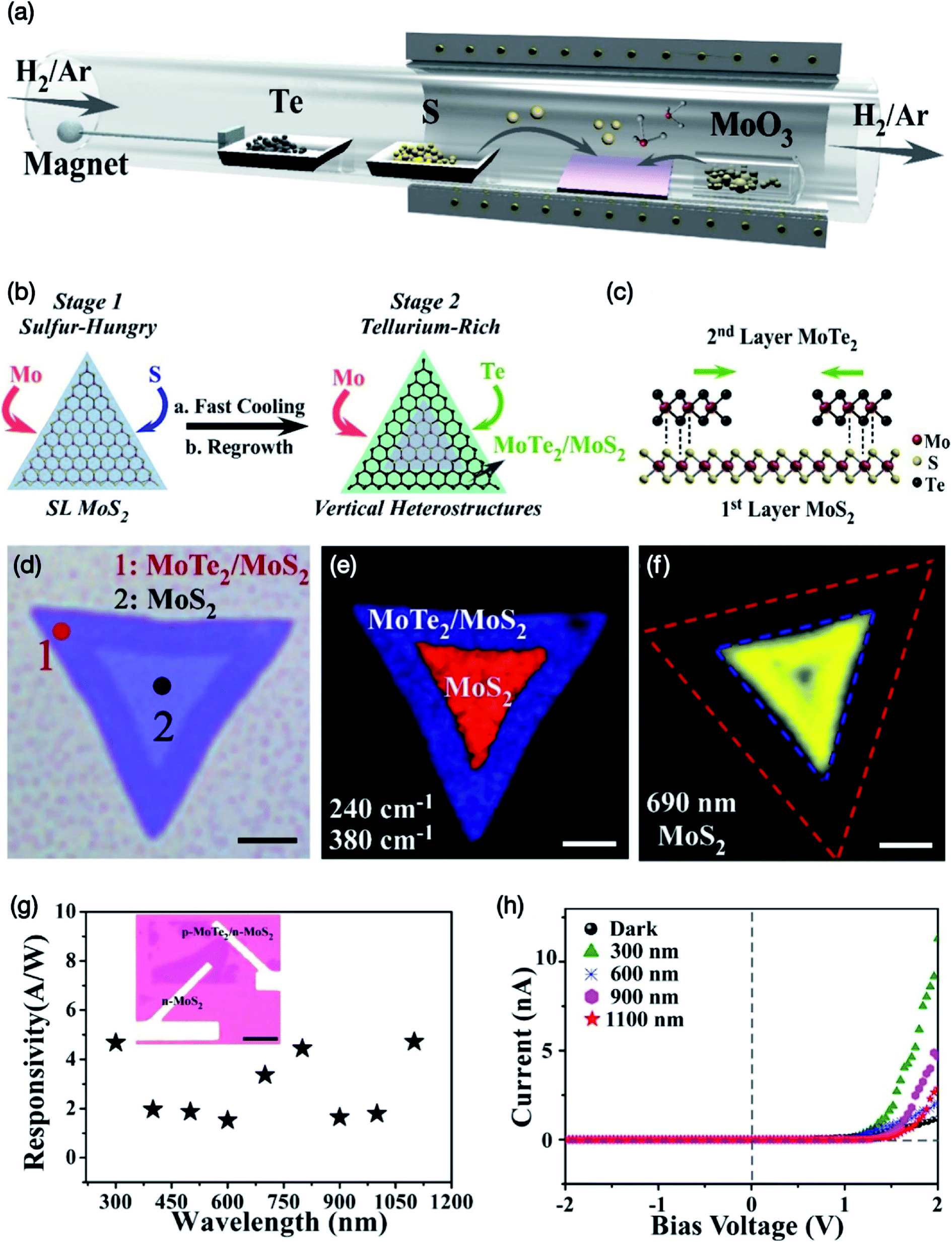 | ||
| Fig. 10 (a) Schematic diagram of experimental set-up showing magnet-assisted CVD growth method for preparing MoTe2/MoS2 heterostructure. (b) Vertically stacking approach of MoTe2/MoS2 bilayer heterostructures. (c) Schematic side view of the MoTe2/MoS2 bilayer heterostructure where Mo atoms are represented in red, S atoms in yellow, Te atoms in black. (d) Optical image of the MoTe2/MoS2 flake. (e) Raman intensity mapping at 240 cm−1 shown in blue and 380 cm−1 in red. (f) PL intensity mapping at 690 nm wavelength where the red dash lines defect the MoTe2/MoS2 heterojunction and the blue dash lines indicates the interface of regions with the inner core and outside ring. (g) Photoresponsivity of MoTe2/MoS2 photodetectors as a function of wavelength between 300 nm to 1100 nm region. (h) I–V current characteristics of the MoTe2/MoS2 photodetectors at different applied bias voltage. Reprinted with permission from ref. 166, copyright © Elsevier. | ||
A significant improvement in mobility was also observed for NbS2/MoS2 vdWH-based Schottky-effect FETs, which yielded a mobility of 800 cm2 V−1 s−1 at room temperature with graphene source/drain (S/D) contacts, compared with the low mobility values of 15–170 cm2 V−1 s−1 for pure MoS2 FETs with Au contacts, depending on the annealing conditions.206 In contrast, lower photoresponsivities were recorded for GaSe/MoS2 vertical heterostructure-based FETs at wavelengths from 300 nm to 670 nm under 6.412 mW cm−2 to 2.169 mW cm−2 optical power, as were a low mobility of 0.026 cm2 V−1 s−1 and a low Ion/Ioff current ratio of 103, compared with pure MoS2 FETs due to the increased scattering of charge transport carriers at the interface of the vdW heterojunctions.207a Atomic layer vdW heterostructure-based photodiodes were fabricated using n-type MoS2 on top of p-type GaSe crystals, which showed photoresponsivity of ∼3 A W−1 at 532 nm when symmetric FL graphene contacts were used.207b However, the asymmetric GaSe/FL graphene and MoS2/Au contacts based vdW photodiodes resulted in a low NEP value of 10−14 W Hz−1/2 because of the reduced dark current and a large LDR of ≈70 dB.
3.6 Interface coupling effect in dual-gated MoS2 phototransistors
Different strategies have been used to improve photoresponse of photodetectors. Deng et al.208 demonstrated that the interface coupling effect (ICE) enhanced photoresponse in fully-depleted silicon-on-insulator (FD-SOI) metal-oxide-semiconductor field-effect transistors (MOSFETs). The thinner Si film-based photodetectors exhibited higher photoresponsivity due to a stronger ICE. CMOS-compatible SOI photodetectors achieved a high photoresponsivity of 3.3 × 10⁴ A W−1. This ICE strategy was also employed for improving the performance of MoS2-based phototransistors. Liao et al.209 first reported interface coupling effect (ICE) phenomenon in dual-gated (DG) MoS2 phototransistors. Both negative top-gate (TG) voltage (VTG) as well as the positive back-gate (BG) voltage (VBG) is simultaneously applied to the MoS2 channel in order to facilitate the trapping of photogenerated holes in the depleted region beneath top-gate. In fabricating DG MoS2 phototransistors, two metal gates were placed on the top and bottom of a MoS2 layer. Fig. 11 shows a 3D schematic and optical microscopic image of a DG MoS2 phototransistor, photoresponsivity (R) of DG MoS2 phototransistor as a function of VBG under different VTG with illumination power density (Pin) of 1.55 mW cm−2 at 550 nm wavelength, Rmax and detectivity (D*) as a function of applied VTG, Pin dependent R with different VBG, MoS2 thickness dependent R and D* values and schematic illustration of ICE in the DG MoS2 phototransistor with positive and negative VTG biases. The DG MoS2 photodetector, having varied thickness between 2.5 nm to 6.5 nm, showed the highest photoresponsivity of 7.7 × 10⁵ A W−1 and detectivity of 1.9 × 10¹⁴ Jones under illumination power density (Pin) of 53 μW cm−2 at 550 nm under VTG = 5.0 V and VBG = 2.0 V. The response and recovery time of the DG MoS2 photodetector decreased from 11.9 s to 8.3 s and 76.2 s to 46.4 s as the VTG decreased from −4 V to −6 V, respectively. The maximum photoresponsivity and detectivity of BG-MoS2 FETs were found to be 7 × 10³ A W−1 and 9.6 × 10¹² Jones, respectively. DG MoS2 photodetectors showed photoresponsivities in 104 to 105 A W−1 range independent of the MoS2 thickness; however, photoresponsivity decreased as the thickness of the MoS2 channel was less than 2.5 nm or more than 6.5 nm. DG MoS2 photodetectors having 2.5 and 6.5 nm thickness exhibit a strong ICE under applied negative VTG and positive VBG. The photoresponse speed of the DG MoS2 phototransistors can be adjusted with ICE. This study showed that the interface coupling effect in the DG MoS2 phototransistors improves the photoelectric performance of photodetectors.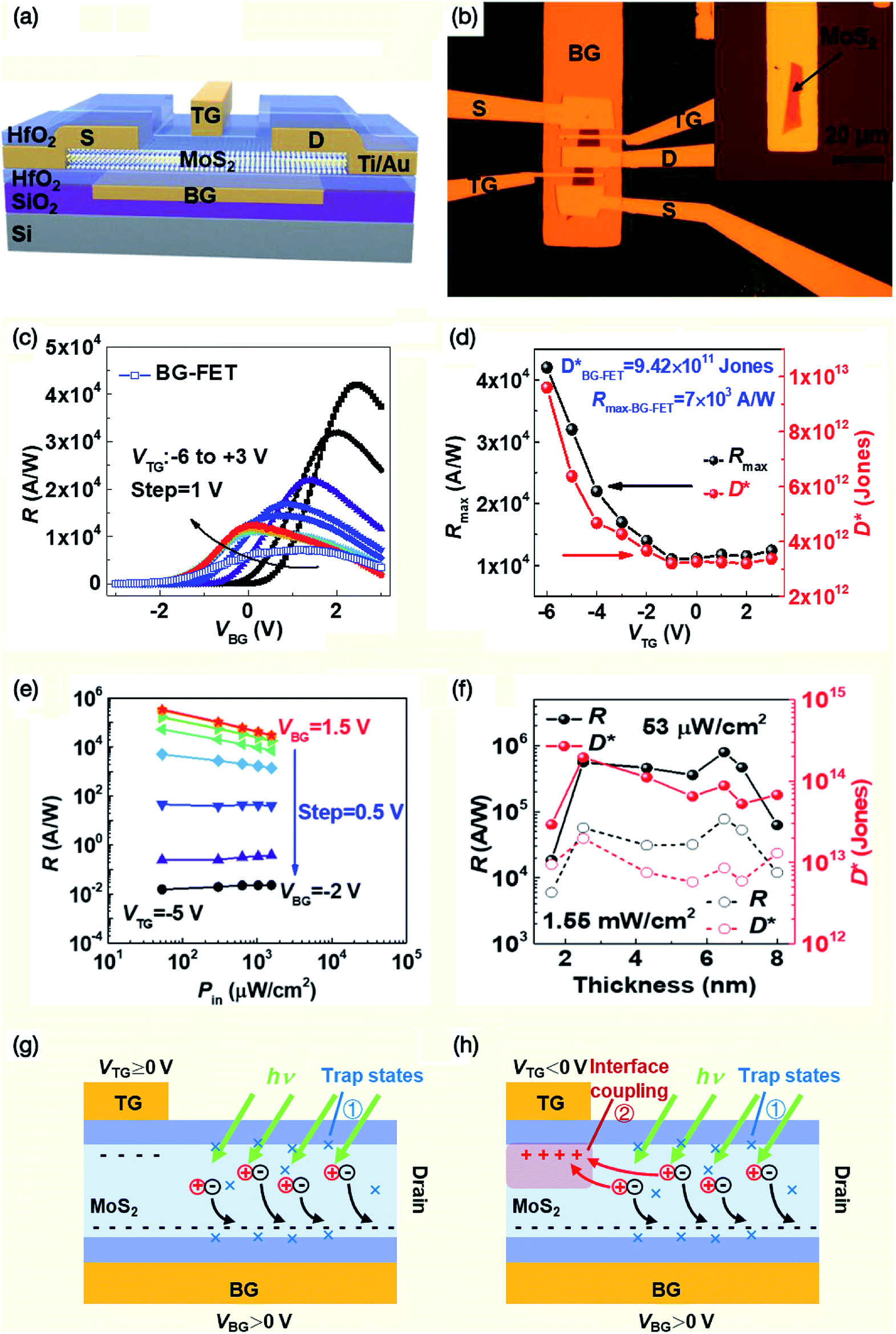 | ||
| Fig. 11 (a) 3D schematic of a dual-gated (DG) MoS2 phototransistor on a Si/SiO2 substrate showing location of top-gate (TG), bottom-gate (BG), source (S), drain (D) and HfO2 layer as a BG dielectric. (b) Optical microscopic image of a DG MoS2 phototransistor. Inset is an optical microscopic image of the ML MoS2 flake. (c) Photoresponsivity (R) of DG MoS2 phototransistor as a function of back-gate voltage (VBG) under different top-gate voltage (VTG) with illumination power density (Pin) of 1.55 mW cm−2 at 550 nm wavelength. Blueline + square symbol represent photoresponsivity of MoS2 BG-FET. (d) The maximum photoresponsivity (Rmax) and detectivity (D*) as a function of applied VTG. (e) Pin dependence of photoresponsivity the DG MoS2 phototransistor with varying VBG at VTG = −5 V. (f) The MoS2 thickness (1.6 to 8 nm) dependence of R and D* under the illumination power density of 53 μW cm−2 (solid sphere) and 1.55 mW cm−2 (open circle). Schematic illustrating generated electron–hole pairs in the DG MoS2 phototransistor with a positive VTG bias (g) and a negative (h) VTG bias in connection with interface coupling effect (ICE). Reprinted with permission from ref. 209, copyright © Wiley. | ||
Flexible photodetectors for wearable applications have been developed from a wide variety of nanomaterials, and their performance is controlled by many conditions, including the material synthesis, atomic layer processing, hybrid heterostructures, device fabrication, measurement wavelengths and incident laser power.64,87,208–214 The performance of MoS2-based photodetectors, such as the detectivity, photoconductive gain, response time and broadband responsivity depends on several factors, including the number of active layers, processing, nature of doping materials, vdW interactions, barrier and junction heterostructures, transport, photocarrier generation and spectral range.215 Additionally, ferroelectric polymers, such as poly(vinylidene fluoride) (PVDF), poly(vinylidene fluoride-trifluoroethylene) [P(VDF-TrFE)] copolymer and poly(vinylidene fluoride-trifluoroethylene-chlorofloroethylene) [P(VDF-TrFE-CFE)] terpolymer are unique organic polymers that have been used in flexible electronics because they offer high piezoelectricity, pyroelectricity and ferroelectricity, tremendous mechanical strength and flexibility to integrate into devices such as transducers, sensors, actuators, nonvolatile ferroelectric random-access memory (NV-FeRAM) and ferroelectric FETs.216 Additionally, in the case of MoS2 photodetectors, these ferroelectric polymers help suppress the dark current, which ultimately improves the photoresponse of photodetectors.137 MoS2-based flexible photodetectors are discussed in the next section.
4. MoS2 based flexible photodetectors for wearable technology
Similar to graphene, applications of flexible atomic layered TMDs have been explored for wearable technologies, from electronics to optoelectronics.36 Flexible photodetectors are expected to be important elements of wearable optoelectronic technology in fields from biomedical imaging to surveillance and high-speed broadband optical communication. Flexible photodetectors have been developed using a variety of nanomaterials, from traditional semiconductors, such as Si, Ge, Se, GaP, InP, CdS and ZnSe,42–49 to newly emerging perovskites,75,76 as a very wide variety of hybrid heterostructures involving polymers, metal oxides, CNTs, graphene, transition metal trichalcogenides, etc.77–89 Similarly, flexible MoS2 atomic layers and MoS2-based hybrid heterostructures have been explored for fabricating photodetectors for the next generation of wearable technologies. The progress made in developing flexible MoS2 photodetectors is summarized in this section.Flexible polymeric substrates based on poly(ethylene terephthalate) (PET), Kapton/polyimide/(PI), poly(methylmethacrylate) (PMMA), poly(ethylene naphthalate) (PEN), poly(dimethylsiloxane) (PDMS) and poly(4-vinylphenol) (PVP) have been generally used for developing wearable electronic and optoelectronic devices due to their inherent mechanical strength and flexibility.23,25,36 In addition, textile fibers and papers have also been considered for developing flexible devices. Zhang et al.217 reported substrate-dependent performance of MoS2 photodetectors owing a dual-photogating effect where rigid silicon carbon (SiC) and flexible Kapton (polyimide) films were used as substrates for developing MoS2 photodetectors. Both SiC and Kapton have strong light absorption, therefore, the dual-photogating effect induced at the interface of the MoS2/SiC or MoS2/Kapton assists in enhancing the photoresponse of MoS2-based photodetectors. Fig. 12 shows the schematic illustrations of MoS2 photodetectors fabricated on updoped SiC and Kapton substrates, their energy level diagrams and the variation of photoresponsivity (R) and on/off ratio (Iphoto/Idark) of rigid MoS2/SiC and MoS2/SiO2/Si photodetectors as well as flexible MoS2/Kapton and MoS2/PET photodetectors as a function of optical power intensity in the UV and visible wavelengths. The bandgap of 2.7 and 3.2 eV and the electron affinity of 4.2 and 1.8 eV for MoS2 and SiC are depicted, respectively. The energy level mismatch at the MoS2/SiC interface yields to a strong built-in electric field (Ein) which assists in separating the photoexcited carriers in MoS2. The enhanced photoresponse was noticed for the MoS2/SiC photodetectors more than those of MoS2/SiO2/Si photodetectors. The energy band diagram in a flexible MoS2/Kapton photodetector shows the valence band of MoS2 as −6.0 eV and conduction band as −4.2 eV and the HOMO level at −5.0 eV and LUMO level at −2.1 eV, versus vacuum. The highest photoresponsivity of ∼104 A W−1 for MoS2/SiC photodetector and the fastest current Ion/Ioff ratio of ∼105 for MoS2/Kapton photodetector were measured at 325 nm laser illumination due to the dual-photogating effect generated at the MoS2/substrate interface. SiC and Kapton substrates improve the photoresponse of MoS2 photodetectors due to the light absorption.
 | ||
| Fig. 12 (a) Schematic illustration of MoS2 photodetector on a SiC substrate. (b) Energy level diagrams of the MoS2 and SiC showing electron affinity and bandgap of MoS2 and SiC. MoS2/SiC interface showing a band structure. (c) Variation of photoresponsivity (R) and (d) on/off ratio (Iphoto/Idark) of rigid MoS2/SiC and MoS2/SiO2/Si photodetectors as a function of optical power intensity in the UV and visible wavelengths. (e) Schematic illustration of MoS2 photodetector on a flexible Kapton substrate. (f) Energy band diagram of a flexible MoS2/Kapton photodetector. (g) Variation of photoresponsivity (R) and (h) on/off ratio (Iphoto/Idark) of flexible MoS2/Kapton and MoS2/PET photodetectors as a function of optical power intensity in the UV and visible regions. Reprinted with permission from ref. 217, copyright © Royal Society of Chemistry. | ||
Transparent poly(4-vinylphenol) (PVP) as the encapsulation layer, as well as a gate dielectric was used by Ma et al.218 for developing flexible MoS2 phototransistors on a polyarylate substrate. PVP thin film having ≥80% transmittance between 400 nm to 900 nm was used. The PVP encapsulation not only increased the mobility but also improved the current Ion/Ioff ratio and subthreshold slope. The photoresponsivity (2 A W−1), as well as the detectivity (3.1 × 10¹² Jones) of MoS2 phototransistors, was increased by two orders of magnitude over the visible to IR range due to the doping effect of hydroxyl groups in PVP. For a comparison, the transparent PVP polymer improved the photoresponsivity of MoS2-based flexible phototransistor devices by ten fold over that of PMMA encapsulated devices. The photodetectors developed from monolayer and bilayer MoS2 encapsulated with a HfO2 layer showed photoresponsivity in the wide range of 10–104 A W−1 and a response time from 10 ms to 10 s.135 These studies show the role of encapsulation in increasing the photoresponse of MoS2-based photodetectors.
Transparent and flexible MoS2 phototransistor arrays using all-organic components with inkjet-printing technology were developed by Kim et al.219 The CVD-grown monolayer MoS2 channel layers were transferred onto a flexible PEN substrate. The all-organic components, including poly(3,4-ethylenedioxythiophene)polystyrenesulfonate (PEDOT:PSS)-based source/drain electrodes, PVP as a gate dielectric layer, and PEDOT:PSS as a top-gate electrode, were consecutively inkjet printed on the monolayer MoS2/PEN substrate. The formation of CVD-grown monolayer MoS2 was confirmed by Raman spectroscopy, XPS, scanning transmission electron microscopy (STEM) coupled with energy dispersive X-ray spectroscopy (EDS), PL spectroscopy, and optical transmittance spectroscopy as demonstrated in Fig. 13(a and b). The optical transmittance of the inkjet-printed MoS2 phototransistors was 76%, compared with 87% for the PEN substrate in the same visible wavelength range. The performance of printed MoS2 phototransistors was not degraded under 1000 repeated bending cycles, as shown by the mobility and SS values for a fixed 5 mm bending radius, which corresponds to 1.26% uniaxial tensile strain along the MoS2 channel length, demonstrating good mechanical stability as shown in Fig. 13(c and d). The mobility and SS values of MoS2 phototransistors measured at bending radii of 15, 11, 7.5, and 5 mm increased as the bending radius decreased. Fig. 13(e and f) shows the photoresponsivity and photodetectivity of transparent MoS2 phototransistors as a function of wavelength over the 405–780 nm region at a fixed laser power density of 57.3 W m−2, a Vgs of 80 V, and a Vds of 10 V. The photoresistivity, detectivity and EQE of MoS2 phototransistors showed wavelength dependence, varying between 0.01 and 0.02 A W−1, 3.0 and 4.8 × 10⁷ Jones, and 1.5 and 6.6%, respectively.
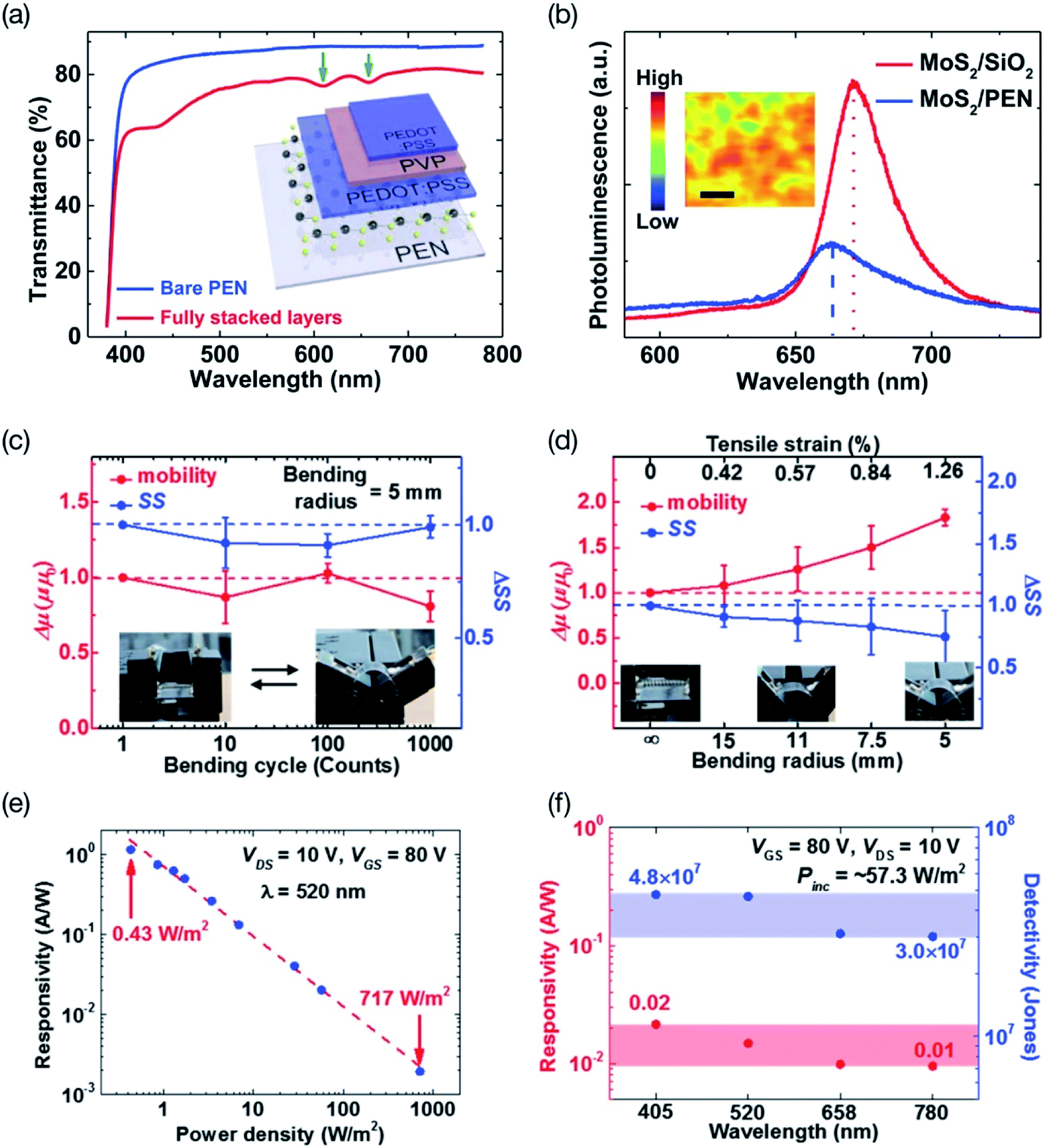 | ||
| Fig. 13 (a) Transmittance spectra of the flexible bare PEN substrate, denoted by the blue line, and fully stacked PEDOT:PSS/PVP/PEDOT:PSS/MoS2/PEN layers, denoted by the red line. The inset is a schematic of the phototransistors with stacked layers. (b) PL spectra of CVD-grown monolayer MoS2/SiO2/Si and MoS2/PEN. The inset is PL intensity mapping at 670 nm (1.85 eV). (c) The variation in mobility and SS values as a function of the number of bending cycles for a 5 mm bending radius, and (d) mobility and SS values at different bending radii of 5, 7.5, 11, 15 mm, and ∞. (e) Variation of photoresponsivity MoS2 phototransistors as a function of power density at 520 nm laser wavelength. (f) Photoresponsivity and photodetectivity of transparent MoS2 phototransistors at different laser wavelengths. Reprinted with permission from ref. 219, copyright © American Chemical Society. | ||
Flexible photodetectors obtained by depositing MoS2 layers on a PI substrate were developed by Lim et al.220 The MoS2 layers were characterized in terms of their uniformity, stoichiometry and structural homogeneity by Raman, AFM, and XPS techniques. The frequency difference of 23.4 cm−1 between the E2g1 and A1g Raman vibration modes of the MoS2 layers indicated few-layer MoS2 thin films. TEM showed the formation of five-layer MoS2 films and an interlayer spacing of 6 Å. The optical transmittance was 90.8% at 550 nm for the MoS2 films deposited on a glass substrate. MoS2 FETs showed a mobility of 14 cm2 V−1 s−1 and an on–off current ratio of 5 × 10². The MoS2 photodetector arrays were also fabricated on a 4-inch SiO2/Si wafer. Fig. 14 shows a photograph of the MoS2 layer on a flexible PI film, XPS spectra, time-dependent photocurrents before and after bending up to 105 bending cycles, and the change in the photocurrent of MoS2-based flexible photodetectors as a function of the bending cycle at 20 V. The visible-light photodetectors exhibited a response time of 13 s and a recovery time of 30 s. MoS2 photodetectors were formed on a flexible PI substrate, and the photocurrent decreased by 5.6% after 105 bending cycles at a bending radius of 5 mm.
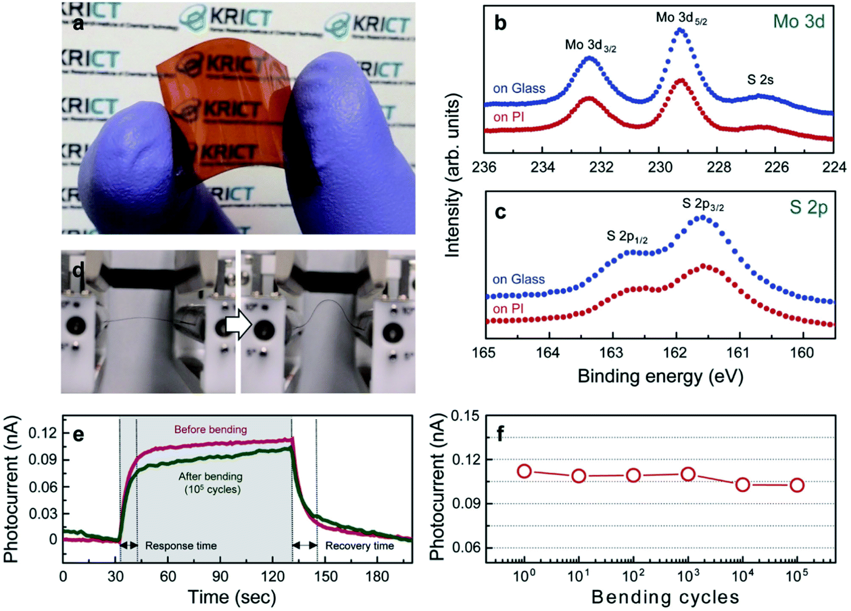 | ||
| Fig. 14 (a) Photograph of the MoS2 layer on a flexible PI film. (b) XPS spectra showing the Mo 3d core level and (c) S 2p core level spectra of MoS2 layers on glass and PI substrates. (d) Bending of a flexible MoS2 layer deposited on a PI substrate at a 5 mm bending radius. (e) Time-dependent photocurrents of MoS2-based flexible photodetectors measured at an incident power of 12.5 mW cm−2 and V = 20 V, before and after bending up to 105 bending cycles. (f) The variation in the photocurrent of the MoS2 photodetector as a function of the bending cycle. Reprinted with permission from ref. 220, copyright © 2016 Wiley-VCH. | ||
Enhancement of the photocurrent and sensitivity has been observed for flexible p-CuO/n-MoS2 heterojunction-based photodetectors.221 The dark current of CuO/MoS2 heterojunction increased from 0.039 nA to 0.12 nA as the tensile strain was increased from 0% to 0.65%, whereas the photocurrent increased to 108 nA under 0.65% tensile strain with 1656 mW cm−2 light intensity, which is 2770-fold increase in the photocurrent over that of the dark current. The photocurrent of the p-CuO/n-MoS2 heterojunction increased 27 times under 0.65% tensile strain compared with that of the strain-free heterojunction at 532 nm, and the sensitivity reached 3.27 × 10⁸ Jones. The photoresponse of a flexible CuO/n-MoS2 heterojunction based photodetector was increased by the piezophototronic effect. Zhang et al.222 fabricated a MoS2 phototransistor on a transparent and flexible biodegradable paper substrate using a gel electrolyte gate dielectric. The gel electrolyte thin layer was coated on top of mechanically exfoliated MoS2 flakes as the gate dielectric. The optical transmittance of the MoS2 phototransistor at 550 nm was 82%, compared with 85% for the bare nanopaper, due to the added passivation layer and gel electrolyte gate dielectric. The MoS2 phototransistor exhibited a photoresponsivity of 1.5 kA W−1 at an illumination power of 10 nW. The MoS2 phototransistor showed high flexibility and optical transparency with great photoresponsivity.
The solution-processed few-layer MoS2 thin films on several flexible substrates, including PI, Al, and Cu foils, cotton thread, and cellulose, carbon, and ceramic paper were developed by Sahatiya et al.223 The growth of layers and morphologies of the MoS2 nanosheets varied depending on the substrate. The photodetectors fabricated from these MoS2 nanosheets showed that the defects introduced during growth control the photocurrent response. Sahatiya et al.224 also fabricated a broadband flexible photodetector using 1D V2O5 NWs and 2D MoS2 flakes covering the UV (365 nm) to NIR (780 nm) region, wherein V2O5 NWs absorb in the UV-visible, and MoS2 absorbs in the visible–NIR regions. The V2O5/MoS2 hybrid device showed a responsivity of 41.5 mA W−1 in the UV, 65.1 mA W−1 in the visible, and 29.4 mA W−1 in the NIR. The same research team225 also developed a flexible photodetector using MoS2/C QD hybrid films. The wide UV-vis-NIR absorbance range originated from the UV absorbance of the C QDs and the visible–NIR region absorbance of MoS2. The MoS2/C QD sensor showed photoresponsivities of 2.62, 8.4, and 18.12 mA W−1 in the NIR, UV, and visible regions, respectively. The MoS2/C QD sensor showed almost no change in photoresponse up to 500 bending cycles. These flexible MoS2/C QD broadband photodetectors can be used for wearable electronics for surveillance purposes.
4.1 MoS2/graphene hybrid heterostructures for flexible photodetectors
The indirect bandgap restricts the photodetection ability of multilayer MoS2. Hybrids of MoS2 atomic layers with gapless graphene have been used to improve the optoelectronic properties by utilizing the high carrier mobility, ultrafast response and broadband absorption of graphene and the generation of electron–hole pairs by MoS2. Ross et al.126 obtained a high carrier mobility (1 × 104 cm2 V−1 s−1) in a graphene/MoS2 hybrid structure by placing monolayer graphene on a multilayer MoS2 nanosheet on a Si/SiO2 substrate. The graphene/MoS2 hybrid-based photodetector showed high photoresponsivities of 1 × 10¹⁰ A W−1 at 130 K under an LED power of 1 fW μm−2 and of 5 × 10⁸ A W−1 at room temperature under an LED power of 6.4 fW μm−2 and gate-tunable photoconductivity with a high photodetection capability. Zhang et al.226 used CVD-grown monolayer MoS2 to develop a graphene/MoS2 hybrid structure-based phototransistor that showed a photoresponsivity of 1.2 × 10⁷ A W−1 at 650 nm under a light power of 0.01 W m−2 and a high photogain of 108. A photoresponsivity of 3.34 × 10³ A W−1 and a detectivity of 1.004 × 10¹² Jones have been observed for graphene/MoS2 hybrid structure-based FETs.227 The phototransistor fabricated from multilayer MoS2 using graphene source/drain electrodes showed a high photoresponsivity of 1 × 10⁴ A W−1 in the wavelength range of 470–600 nm.228Chen et al.229 developed n–n-type vdWHs using multilayer MoS2 coated with a layer of nitrogen-doped graphene QDs (N-GQDs) to complement each other with their strong characteristics to improve the carrier mobility. In this hybrid structure, MoS2 was used to generate photoexcited holes, while the GQDs working as a gain material contributed to the recirculation of photoexcited carriers at the heterojunction interface. Additional photocarriers were also created by the reabsorption of light emitted from the GQDs by MoS2. Fig. 15 shows a schematic of the MoS2/GQD heterostructure-based phototransistor, a comparison of the drain current (Id) versus source–drain voltage (Vds) curves of pristine MoS2 and MoS2/GQD hybrid phototransistor devices in the dark and under light illumination, and the photoresponse speed and incident light power-dependent photoresponsivity of MoS2/GQD vdWH-based phototransistors. In the case of the MoS2 phototransistor, the drain current increased to 10.15 μA at a 405 nm wavelength under an incident laser power of 30.1 μW, with a source–drain voltage (Vds) of 1.68 V; this drain current was 1000 times larger compared with the 11 nA current recorded in the dark state. The MoS2 phototransistor showed a sensitivity up to 5 nW and rise/fall times longer than 50 s. The MoS2 phototransistor showed the highest photocurrent of 16.2 μA at 50 nW and photoresponsivity of 800 A W−1 at 70 V. The MoS2/GQD hybrid phototransistor showed a significant change in the drain current (Id) versus source–drain voltage (Vds) curves, a higher drain current and a faster photoresponse speed compared with the pristine MoS2 phototransistor. The photocurrent of the MoS2/GQD hybrid phototransistor reached 0.55 mA at a gate bias of 80 V. The MoS2/GQD heterostructure-based photodetector showed a photoresponsivity of 1.6 × 10⁴ A W−1 at 80 V under an incident power of 50 nW and a photoconductive gain of 2.4 × 10⁷ electrons per photon. The high performance of MoS2/GQD heterostructure-based photodetectors occurs due to their increased light absorption and the effective generation of electron–hole pairs between the GQDs and MoS2.
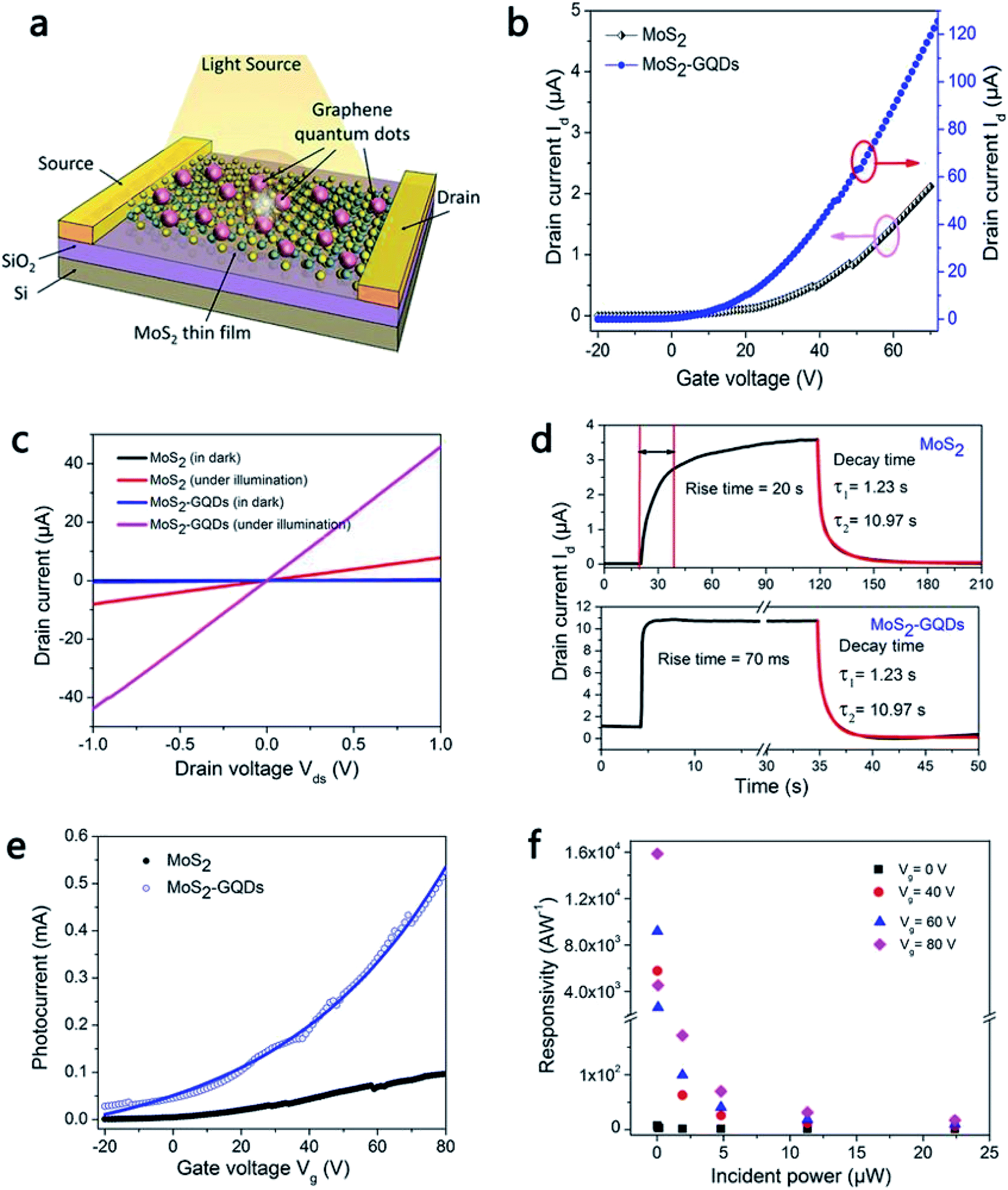 | ||
| Fig. 15 (a) Schematic of the MoS2/GQD heterostructure-based phototransistor. (b) Current vs. voltage curves of MoS2 and MoS2/GQD phototransistor devices. Here, Id is the drain current, and Vds is the source–drain voltage = 1 V. (c) Drain current versus source–drain voltage curves in the dark and under light illumination for MoS2 and MoS2/GQD phototransistors, measured at a 405 nm wavelength under an incident light power of 17 μW. (d) Photoresponse times of MoS2 (top) and MoS2/GQD (bottom) phototransistors. (e) Photocurrent versus back gate voltage curves for MoS2 and MoS2/GQD phototransistors, measured under an incident light power of 30.1 μW. (f) Incident light power-dependent photoresponsivity of MoS2/GQD phototransistors. Reprinted with permission from ref. 229, copyright © Springer Nature Publishing. | ||
Large-area MoS2 films on monolayer graphene were developed by Chen et al.230 by adding hydrogen gas during the CVD growth process, which resulted in centimeter-long monolayer MoS2 continuous films on graphene. Hydrogen addition prevented the degradation of monolayer graphene by decreasing the oxidation. The MoS2/graphene-based photodetector showed a photoresponsivity as high as 2.4 A W−1 under 532 nm illumination and a 135 μW power density. Flexible photodetectors, consisting of an rGO fiber and MoS2 nanosheet hybrid composite, showed significant enhancement of the photocurrent.231a The Zn-doped MoS2/rGO hybrid fiber-based flexible photodetectors showed a photoresponsivity of 5.73 A W−1 at laser power density of 125.2 W m−2 using a bias voltage of 2 V. The same research group also reported one-step synthesis for preparing Zn-doped MoS2 photodetector using Zn(II)-tetrakis(4-hydroxyphenyl)-porphyrin [Zn(II)THPP] as a dopant loaded seeding promoter.231b The Zn-doped MoS2 thin films were transferred onto a PET substrate to fabricated flexible photodetectors. The electrical resistance of the flexible photodetector increased 13% after 10000 bending cycles at a bending radius of 3 cm while resistance increased 10% at a bending radius of 1 cm, demonstrating good mechanical stability of the flexible photodetectors. The photocurrent of Zn-doped MoS2 photodetectors was found to increase from 0.05 μA to 2.62 μA as the applied voltage was raised from 1 V to 40 V at a power density of 125.2 W m−2 and a similar trend was observed for the photoresponsivity. The photocurrent and photoresponsivity of the Zn-doped MoS2 photodetectors can be controlled by adjusting the Zn doping concentration. Asad et al.232 used MoS2 nanoparticle (MoS2 NP)-decorated graphene nanoribbons (GNRs) to develop flexible phototransistors. In the GNR–MoS2NP hybrid, the GNRs function as carrier transport channels, whereas the MoS2 NPs offer high gain absorption. The MoS2 NPs also generate electron–hole pairs, which are separated at the GNR and MoS2 NP interface and result in electron transfer from the MoS2 NPs to the GNRs. The flexible GNR–MoS2 hybrid photodetector showed a photoresponsivity of 66 A W−1, a fast rise time of 5 ms and a decay time of 30 ms under 385 nm illumination and a 2.1 μW power density. The photoresponsivity of the GNR–MoS2 hybrid photodetector was 1.3 × 10⁵ times larger than that of the pristine graphene photodetector and 104 times larger than that of the pristine MoS2 phototransistor. The hybrid photodetector also showed high stability for a 6 mm bending radius. De Fazio et al.233 developed visible-light flexible photodetectors using CVD-grown single-layer graphene (SLG) and single-layer (1L) MoS2 on flexible PET substrates. Fig. 16 is a schematic of a flexible SLG/1L MoS2 photodetector on a flexible PET substrate and a photograph of the photodetector showing the optical transparency and flexibility. The polymer electrolyte-gated flexible SLG/1L MoS2 photodetector showed an external photoresponsivity of 45.5 A W−1 and an internal photoresponsivity of 570 A W−1 at 642 nm, a photoconductive gain of 4 × 10⁵, and >82% optical transparency. The flexible photodetectors showed mechanical durability upon bending at a 1.4 cm bending radius. The photoconductive gain increased by nearly one order of magnitude from 0.1 to 1.0 V, and the photoresponsivity reached 45.5 A W−1 at a Vds of 1 V. Therefore, the photoconductive gain of the SLG/1L MoS2-based heterostructure photodetector being four orders of magnitude larger than that of the 1L MoS2 photodetector developed without any SLG showed that the SLG/1L MoS2 heterostructure is important for high photoresponsivity.
 | ||
| Fig. 16 (a) Schematic of the single-layer graphene (SLG)/1L MoS2 photodetector on a flexible PET substrate. (b) Photograph of the flexible photodetector showing optical transparency. The inset is an optical image of 4 photodetectors with different channel lengths. Reprinted with permission from ref. 233, copyright © 2016 American Chemical Society. | ||
Photodetector devices using a MoS2/graphene hybrid pattern formed by the soft-lithographic patterning technique were reported by Kang et al.234 The cross-stacked MoS2/graphene patterns were transferred onto a flexible PET substrate for fabricating flexible photodetectors. Fig. 17 shows a schematic of the formation of cross-stacked MoS2/graphene patterned nanostructures. The various fabrication steps involve the CVD growth of MoS2 nanosheets on a 5,10,15,20-tetrakis(4-hydroxyphenyl)-21H,23H-porphyrin (p-THPP) promoter layer, transfer and patterning of the MoS2 nanosheets using a PDMS mold, CVD growth of a graphene layer on Cu foil, transfer of the graphene layer onto a 300 nm thick SiO2 substrate, and transfer of the graphene layer onto the top of the MoS2 patterns by using a dimethyl sulfoxide (DMSO)-coated PDMS mold—the same process that was eventually employed for the transfer and patterning of the MoS2 film. The SEM images confirmed the cross-stacked MoS2/graphene line patterns with a width of 7 μm. The Raman peak difference between the E2g1 and A1g vibration modes of MoS2 was estimated to be 20 cm−1, which indicated the formation of monolayer MoS2 patterns.
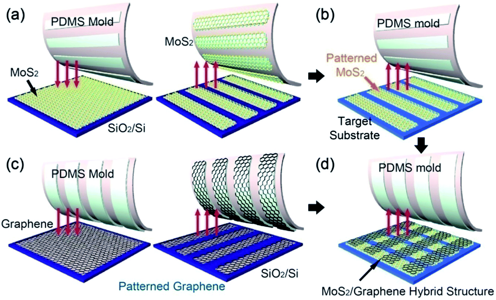 | ||
| Fig. 17 Schematic of the fabrication steps for cross-stacked MoS2/graphene patterned nanostructures. (a) CVD growth of MoS2 nanosheets on a SiO2 substrate (left), and pattern fabrication on the MoS2 layer within a target area (right). (b) Transfer of MoS2 patterns on the PDMS mold onto a target substrate. (c) CVD growth of a graphene layer. (d) Transfer of graphene patterns on the PDMS mold to the top of MoS2 patterns on the target substrate. Reprinted with permission from ref. 234, copyright © Elsevier. | ||
The photoresponsivities for cross-stacked MoS2/graphene hybrid photodetectors containing monolayer, bilayer, and trilayer MoS2 films increased linearly as a function of the bias voltage from (10 to 50) V. The trilayer MoS2 film-based hybrid photodetector showed the highest photoresponsivity compared with the monolayer and bilayer MoS2 films, a value of 5 A W−1 at a bias voltage of 2 V. Fig. 18 shows optical microscope images of cross-stacked patterns of MoS2/graphene based on MoS2 patterns formed by the soft-lithographic patterning technique, photographs of MoS2/graphene hybrid patterns on a flexible PET substrate before and after the bending test, and the photoresponsivity of flexible MoS2/graphene hybrid photodetectors as a function of the number of bending cycles at a bending radius of 9 mm and a 1.0 V bias. The mechanical stability of cross-stacked patterns of graphene/MoS2 photodetector devices fabricated on flexible PET substrates was evaluated under various bending cycles. The photocurrent of the MoS2/graphene hybrid photodetector with MoS2 patterns 10 μm in width was measured between 1 and 10000 bending cycles. The photocurrent of the device decreased from 4.3 to 3.7 A as a function of the number of bending cycles. The smallest reduction in the photoresponsivity with increasing number of bending cycles was observed for the 10 μm wide MoS2 patterns due to the lower compressive stress. Graphene has also been used in developing flexible photodetectors with atomic layered materials. Graphene/tin monosulfide (SnS) hybrid structure-based photodetectors further substantiated that a high photoresponsivity of 1.7 × 10⁴ A W−1 under an optical light intensity of 1.2 mW m−2 can be achieved in flexible graphene/SnSe/graphene-based photodetectors and demonstrated no change in photoresponse after 25 bending cycles, indicating high mechanical strength of the devices.65
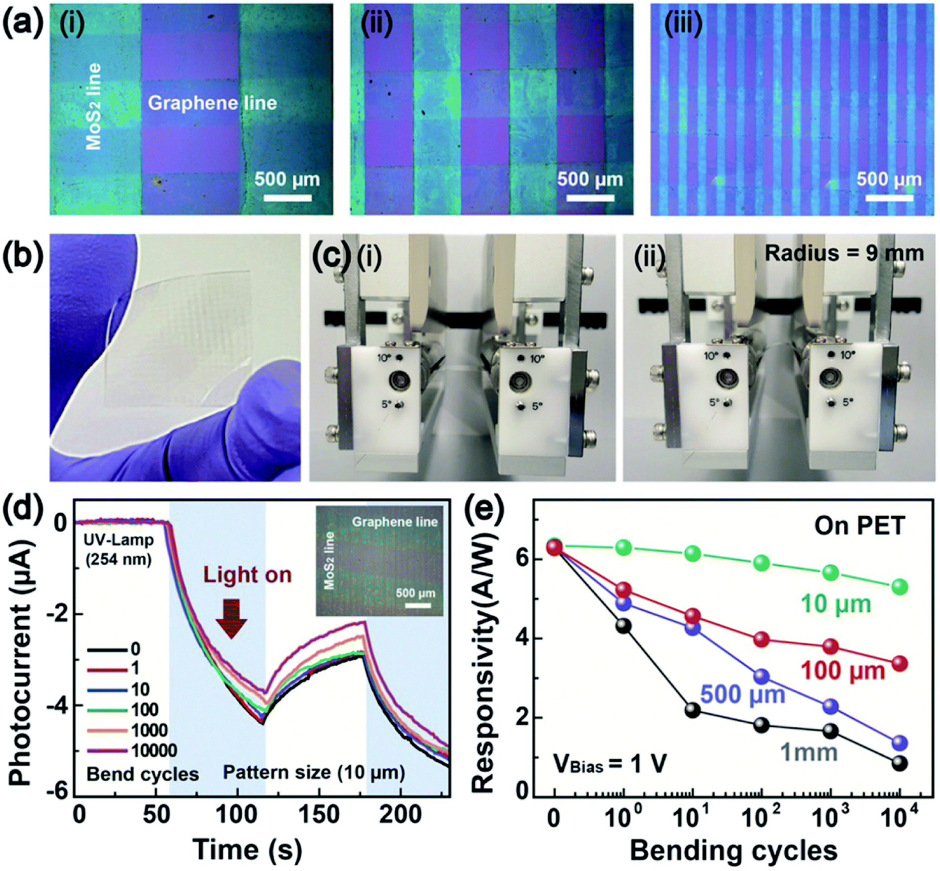 | ||
| Fig. 18 (a) Optical microscope images of cross-stacked patterns of MoS2/graphene based on MoS2 patterns with widths of (i) 1 mm, (ii) 500 μm, and (iii) 100 μm, where the graphene patterns have a fixed width of 500 μm. (b) Photographic image of cross-linked MoS2/graphene hybrid patterns on a flexible PET substrate developed by the soft-lithographic patterning technique. (c) Photographs of MoS2/graphene hybrid patterns on a flexible PET substrate (i) before and (ii) after the photodetector device bending test. (d) Photocurrent as a function of time for a flexible MoS2/graphene hybrid photodetector under 1–10000 bending cycles. The inset shows an optical image of cross-stacked patterned MoS2 (width = 10 μm) and graphene (width = 500 μm). (e) Photoresponsivity of flexible MoS2/graphene hybrid photodetectors as a function of bending cycle (1–10000), where the photodetectors have 1 mm, 500 μm, 100 μm, and 10 μm pattern sizes for the MoS2 layers. The bending test was conducted at a bending radius of 9 mm and a 1.0 V bias voltage. Reprinted with permission from ref. 234, copyright © Elsevier. | ||
Polymer electrolytes have been used for developing flexible MoS2 photodetectors. Sun et al.235 fabricated four phototransistor arrays with 100, 200, 500, and 1000 μm channel lengths in one flexible photodetector device based on a vertically stacked MoS2/graphene thin film deposited on a PET substrate. A polymer electrolyte consisting of PEO:LiClO4 in an 8:1 ratio was used to fabricate a flexible side-gated photodetector. The flexible photodetector based on the MoS2/graphene film showed an external responsivity of 3.5 A W−1 at −1 V (Vgs) under a 60 μW incident power. The MoS2/graphene thin film had a transmittance of 10.5% at 520 nm, and the internal photoresponsivity of the photodetector reached 33.3 A W−1. The photocurrent of the MoS2/graphene film can be adjusted in the 0 to 300 μA range.
4.2 MoS2/carbon nanotube hybrid heterostructures for flexible photodetectors
CNTs show large optical absorption compared with traditional semiconductors; therefore, photodetection can be further improved by using CNTs in hybrid heterostructures.236,237 CNT-based hybrid broadband photodetectors have been fabricated with a variety of functional materials, including Si, GaAs, fullerenes, graphene, ZnO, PbS, and perovskites.238–249 A negative photoresponsivity on the order of 108 A W−1 has been reported in fullerene-sensitized aligned CNTs at room temperature.250 Highly flexible photodetectors based on CNTs have been demonstrated for wearable technologies.251–254 The outstanding electronic and optical properties have been utilized by integrating CNTs with MoS2 atomic layers to develop flexible CNT/MoS2 hybrid broadband photodetectors.Photodetectors have been developed using few-layer MoS2/SWCNT hybrids,255 which showed high photoresponsivities of 100 to 1000 A W−1 at a 0.1 V bias voltage in the 500–700 nm visible range. Specifically, the MoS2/SWCNT hybrid structure exhibited a photoresponsivity of 300 A W−1 at 532 nm under a Vg of 0 V. Large-area MoS2, WS2, and MoSe2 device arrays were fabricated by Li et al.256 MoS2 channels and MoS2/CNT hybrid electrodes were simultaneously deposited on a CNT-patterned substrate by the CVD method. MoS2–MoS2/CNT devices showed ohmic contacts between MoS2 channels and MoS2/CNT hybrid electrodes and exhibited better mechanical stability as well as photoresponsivity than gold-contacted devices, indicating the suitability of the MoS2–MoS2/CNT hybrid for flexible electronic devices. Highly flexible pixel arrays based on MoS2–MoS2/CNT hybrid photodetectors were developed. Fig. 19 shows the flexible MoS2–MoS2/CNT hybrid film-based photodetector pixel array, photocurrent response at zero gate voltage, and image patterns recorded using the MoS2–MoS2/CNT photodetector pixel array. The flexible MoS2–MoS2/CNT photodetector arrays were deposited on a 3 μm thick flexible SU-8 substrate. The MoS2–MoS2/CNT device showed a current below 10−11 A at a bias voltage of 0.5 V. The MoS2–MoS2/CNT devices showed a detectivity of 2.4 × 1010 cm Hz−1/2 W−1. The 160 photodetector pixels formed with MoS2–MoS2/CNT devices were arranged in 16 columns × 10 rows. Both L- and T-shaped image patterns were recorded by the pixel array.
 | ||
| Fig. 19 Flexible MoS2–MoS2/CNT hybrid photodetectors. (a) Flexible MoS2–MoS2/CNT hybrid film-based electronic device array attached to the surface of a glass tube. (b) I–Vds curves of the MoS2–MoS2/CNT hybrid device at 442 nm under different intensities of light illumination. (c) Photocurrent response of the MoS2–MoS2/CNT device as a function of time. (d) Schematic representation of a photodetector pixel array of MoS2–MoS2/CNT hybrid photodetectors. (e) L- and T-shaped image patterns (row vs. column) recorded using the MoS2–MoS2/CNT photodetector pixel array. Reprinted with permission from ref. 256, copyright © Wiley-VCH. | ||
4.3 MoS2/2D TMD hybrid heterostructures for flexible photodetectors
MoS2-based vdWHs have been extensively studied for developing photodetectors, as discussed in the previous section.195–206 The electronic and optoelectronic properties of MoS2-based FETs and photodetectors have been dramatically improved by integrating atomic layered MoS2 with other vdW structures, such as 2D graphene, h-BN and TMDs. Huo et al.257 developed a phototransistor from multilayer MoS2/WS2 vdWHs that exhibited an on/off switching ratio >105, an electron mobility of 65 cm2 V−1 s−1, and a photoresponsivity of 1.42 A W−1, enhanced properties compared with multilayer MoS2 or WS2 transistors. Xue et al.164 used vertical heterojunction arrays of few-layer MoS2/WS2 to develop flexible photodetectors. HRTEM and AFM images indicated three layers of MoS2 (∼2.1 nm) and five layers of WS2 (∼3.9 nm) in the heterostructure layered films. MoS2/WS2 heterojunction-based FETs were fabricated on a rigid SiO2/Si substrate. Flexible MoS2/WS2 heterojunction photodetector arrays were also fabricated on a PDMS substrate. Fig. 20 shows a schematic of the MoS2/WS2 vertical heterojunction-based phototransistor, current–voltage plot, time-dependent photocurrent of the MoS2/WS2 vertical heterojunction at different incident powers during laser switching on/off, photographic image of the flexible MoS2/WS2 vertical heterojunction photodetector arrays on a PDMS substrate and time-dependent photocurrent of the flexible MoS2/WS2 vertical heterojunction photodetector device on the PDMS substrate at different incident laser powers. The MoS2/WS2-based photodetector showed a photoresponsivity of 2.3 A W−1 at a 450 nm wavelength.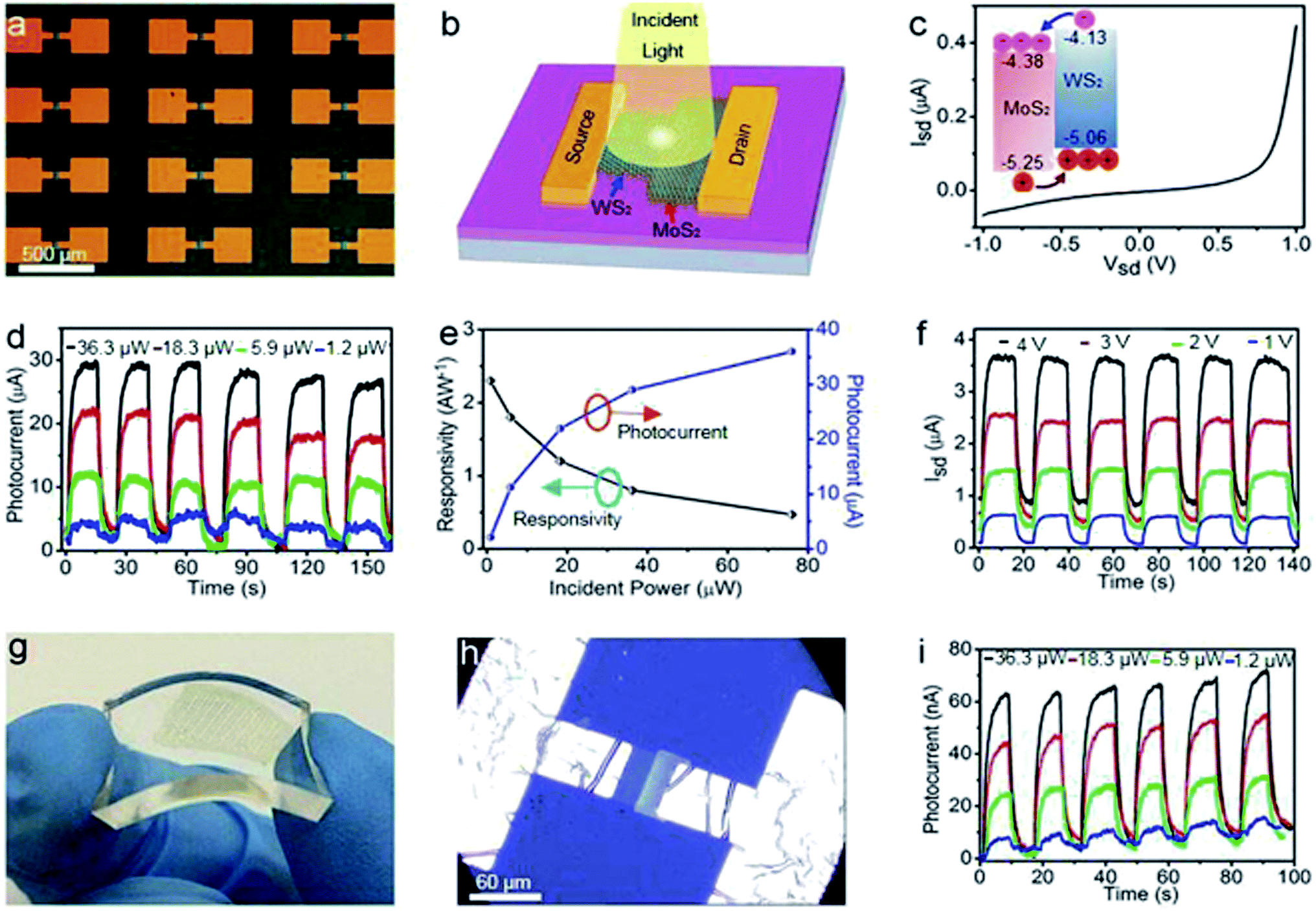 | ||
| Fig. 20 (a) Vertical heterojunction arrays fabricated from few-layer MoS2/WS2 on a SiO2/Si substrate. (b) Schematic illustration of the MoS2/WS2 vertical heterojunction-based phototransistor. (c) Current–voltage plot of a MoS2/WS2 vertical heterojunction-based phototransistor without illumination. The inset indicates the band alignment for few-layer MoS2 and WS2. (d) Time-dependent photocurrent of the MoS2/WS2 vertical heterojunction at different incident powers. (e) Photocurrent and photoresponsivity as a function of incident light power at a 405 nm wavelength. (f) Time dependence of the photocurrent based on the MoS2/WS2 vertical heterojunction photodetector during switching on/off of the laser with varying source–drain voltage (Vsd) from 1 to 4 V. (g) Photographic image of the flexible MoS2/WS2 vertical heterojunction photodetector array on a PDMS substrate. (h) Optical microscope image of a single flexible MoS2/WS2 vertical heterojunction photodetector device on a PDMS substrate. (i) Time-dependent photocurrent of the flexible MoS2/WS2 vertical heterojunction photodetector device on the PDMS substrate at different incident laser powers. Reprinted with permission from ref. 164, copyright © 2017 American Chemical Society. | ||
In another study, Lin et al.258 fabricated flexible vdW photodiodes on flexible PET substrates using monolayer n-MoS2/few-layer p-WSe2 heterojunctions. The photoresponsivity of the MoS2/WSe2 photodiode increased by 86% at −0.62% compressive strain in the MoS2 armchair direction due to realignment of the energy band at the MoS2/WSe2 interface caused by the strain-induced piezoelectricity. The MoS2/WSe2 photodiode showed a photoresponsivity of 3.4 mA W−1. The PL peak intensity of CVD-grown monolayer MoS2 increased by three orders of magnitude after 15 min of TFSI chemical treatment. This study demonstrated that strain-tunable 2D TMD-based vdWHs could be used for developing optoelectronic devices. The photoresponse of flexible MoS2/WSe2 vdWH-based photodiodes was enhanced by the piezophototronic effect. Alloys of TMDs have been explored for developing flexible photodetectors. In another study, Wu et al.264 also demonstrated improved photoresponse of flexible monolayer MoS2 due to the piezophototronic effect for strain-gated photodetectors. The polarization charges induced by the applied strain can change the separation of photogenerated carriers and their transport at the interface between MoS2 and metal allowing tuning of photoresponse. The strain-induced flexible monolayer MoS2 photodetector showed high photoresponsivity of 2.3 × 10⁴ A W−1, which is 26 times larger photoresponsivity compared with monolayer MoS2 phototransistors172 due to the piezophototronic effect. The current (Ids) monolayer MoS2 increased by 2.5 times, from 90 nA in dark to 220 nA under 4.297 mW cm−2 optical power intensity at a drain voltage of −2 V. The photocurrent was 40 nA at 3.4 μW cm−2 power intensity under strain of −0.38%, which increased to 207 nA at 4.29 mW cm−2 power intensity under increased strain of −0.45%. Zheng et al.259 developed Mo0.5W0.5Se2 alloy-based photodetectors on a SiO2/Si rigid substrate and a PI flexible substrate for photodetection over a broadband spectrum ranging from the UV to NIR region (370 nm to 808 nm). The Mo0.5W0.5Se2 photodetectors on the SiO2/Si substrate exhibited a photoresponsivity of 77.1 A W−1 and a detectivity of 1.1 × 10¹² Jones with a rapid response speed of 8.3 ms, whereas the photodetector on the flexible PI substrate showed a photoresponsivity of 63.5 A W−1 and a detectivity of 3.56 × 10¹² Jones. The Mo0.5W0.5Se2 photodetectors showed no noticeable degradation in performance over 100 bending cycles, showing their suitability for flexible optoelectronic devices.
4.4 MoS2/ZnO hybrid heterostructures for flexible photodetectors
Ultrahigh photoresponsivity has been observed in ZnO-based hybrid heterostructures, and flexible broadband photodetectors have been fabricated using ZnO nanostructures (NWs, nanorods, QDs, nanoparticles) combined with other functional nanomaterials, including graphene, CNTs, carbon nanodots, Au, Cu, ZnS, CdO, SnO2, and Zn2SnO4, for wearable technologies.52–54,260–271 Hybrid heterostructures of ZnO with MoS2 have similarly been used to develop photodetectors. The electronic and optoelectronic properties of MoS2 atomic layers have been improved by ZnO doping. A photoresponsivity of 3.18 × 10³ A W−1 and a detectivity of 5.94 × 10¹² Jones have been observed for the ZnO-doped MoS2 photodetector at a wavelength of 520 nm due to the suppression of the recombination rate of photocarriers induced by ZnO doping.272 Nazir et al.273 used ZnO QD-decorated multilayer MoS2 nanosheets to develop ZnO QD/MoS2 heterostructure-based photodetectors. The field-effect mobility of ML MoS2 increased from 5.75 to 25.09 cm2 V−1 s−1 after decorating ML MoS2 with ZnO QDs due to the charge transfer from the deposited ZnO QD thin layer to the surface of the pristine ML MoS2 nanosheet. The ML MoS2 photodetector showed a photoresponsivity of 1913 A W−1 at a VBG of 30 V and a Vds of 1 V at 220 nm under an incident laser power of 11 mW cm−2, which increased to 2267 A W−1 under similar conditions after decorating the ML with a ZnO QD thin layer. The flexible MoS2/ZnO/PEN photodetectors showed an Ion/Ioff current ratio of 104, compared with 103 for the pure ZnO/PEN photodetector.274 The highest photocurrent was obtained for the device with a 5 wt% MoS2 layer. The Ion/Ioff current ratio increased from 8840 to 17800 for 0 to 5 wt% MoS2 in the MoS2/ZnO hybrid structure along with the highest photocurrent and photoresponsivity values for the photodetectors. Pak et al.275 reported a photoresponsivity of 14.9 mA W−1 at 1100 nm for the α-IGZO photodetector capped by a MoS2 layer, which was five times higher compared with the pure α-IGZO photodetector with no MoS2 layer. Yang et al.276 used few-layer MoS2 (bandgap of 1.7 eV) with amorphous indium–gallium–zinc oxide (InGaZnO: α-IGZO) (bandgap of 3.0 eV) to develop a hybrid heterostructure-based phototransistor. The MoS2/α-IGZO hybrid formation imparted enhanced visible light absorption and a high carrier mobility. The band alignment at the heterostructure junction facilitated the transfer of electrons generated by visible light within the upper few-layer MoS2 to the underlying α-IGZO layer. The photocurrent of the MoS2/α-IGZO heterostructure-based phototransistors was four orders of magnitude higher than that of the MoS2 phototransistor at an incident laser power of 1.0 μW; the photoresponsivity was 1.7 A W−1 at a wavelength of 520 nm, and the extrapolated photoresponsivity exceeded 103 A W−1 under an incident laser power of 1.0 pW. The MoS2/α-IGZO phototransistors showed an Ion/Ioff current ratio of 105 and photoresponse times of 2.6 s and 1.7 s.
The morphology of nanomaterials also plays an important role in controlling the electrical properties. Lee et al.277 reported different ZnO morphological nanostructures, such as NWs, nanostars (NSs), and nanoflowers (NFs), which were hydrothermally grown on graphene monolayer and MoS2 multilayer films by adjusting the pH of the solution, and used these ZnO hybrid nanostructures to fabricate photodetectors. ZnO-based NWs, NSs, and NFs were obtained at pH values of 6.53, 8.18, and 9.18, respectively, and characterized by field-emission (FE)-SEM, resonant Raman spectroscopy, and XPS methods. The photodetectors fabricated from ZnO NWs/graphene, ZnO NSs/graphene, and ZnO NFs/graphene showed high photoresponsivity values of 145, 302, and 350 A W−1, respectively. However, the photodetectors fabricated from ZnO NW/MoS2, ZnO NS/MoS2, and ZnO NF/MoS2 hybrids showed very low photoresponsivities of 7.91 × 10⁻⁶, 1.02 × 10⁻⁴, and 8.99 × 10⁻⁴ A W−1, respectively. The EQE of photodetectors developed from ZnO NWs, NSs, and NFs in combination with graphene were 5.14 × 10⁴, 1.07 × 10⁵, and 1.24 × 10⁵%, compared with 2.81 × 10⁻³, 3.63 × 10⁻², and 3.19 × 10⁻¹% for ZnO NWs, NSs, and NFs with MoS2, respectively. Fig. 21 shows a photograph of the ZnO NF/MoS2 photodetector fabricated on a flexible PI substrate, time-dependent photocurrents of hybrid photodetectors developed from ZnO NWs, ZnO NSs, and ZnO NFs along with graphene and MoS2, and the variation in the photocurrent of the ZnO NF/graphene hybrid and ZnO NF/MoS2 hybrid as a function of the bending cycle. The photocurrents of the ZnO NW, NS, and NF hybrids with graphene decrease, whereas the photocurrents of the ZnO NW, NS, and NF hybrids with MoS2 increase under UV illumination at 256 nm owing to the difference in the electronic structures of graphene and MoS2. The photocurrent of the ZnO hybrid photodetectors shows an increasing trend of ZnO NWs < NSs < NFs, regardless of whether graphene or MoS2 is used, because of the increased oxygen vacancies induced by adjusting the pH. The response and decay times were 10 and 67 s for the ZnO NF/graphene hybrid and 61 and 90 s for the ZnO NF/MoS2 hybrid-based photodetector devices, respectively. The photocurrent decreased by 74% for the ZnO NF/graphene hybrid and by 76% for the ZnO NF/MoS2 hybrid-based devices from the initial values after 10000 bending cycles at a bending radius of 6 mm.
 | ||
| Fig. 21 (a) Photograph of the ZnO NF/MoS2 photodetector fabricated on a flexible PI substrate. (b) Time-dependent photocurrents for ZnO NW/graphene, ZnO NS/graphene, and ZnO NF/graphene hybrids measured at 1 V. (c) Time-dependent photocurrents for ZnO NW/MoS2, ZnO NS/MoS2, and ZnO NF/MoS2 hybrids measured at 1 V. (d) The change in the photocurrent of the ZnO NF/graphene hybrid (red) and ZnO NF/MoS2 hybrid (blue) as a function of the bending cycle. Insets show the bending process of photodetectors at a bending radius of 6 mm. Reprinted with permission from ref. 277, copyright © 2017 American Chemical Society. | ||
Flexible photodetectors have been developed using MoS2 and graphitic carbon nitride (g-C3N4) hybrid thin films on a paper substrate, as reported by Velusamy et al.278 The dark current of MoS2 decreased as the amount of g-C3N4 increased in the hybrid films because of the resistivity of g-C3N4, although the photocurrent was significantly improved due to the photocarriers generated under light illumination. The photocurrent of the MoS2/g-C3N4 hybrid increased linearly as a function of increasing laser power density, yielding Ion/Ioff current ratios of 4 × 10³ and 1 × 10⁴, photoresponsivities of 700 mA W−1 and 4 A W−1, and detectivities of 8 × 10¹⁰ Jones and 4 × 10¹¹ Jones at 532 nm and 365 nm wavelengths under laser power densities of 0.225 W cm−2 and 0.5 W cm−2 for MoS2/g-C3N4 (5:5) hybrid thin film, respectively. The photodetectors showed stability, retaining 90% of their initial photocurrent after a time period of 3000 s. The MoS2/g-C3N4 (5:5) hybrid film-based photodetectors showed no significant decrease in the photocurrent after bending the thin films to radii of 10, 7, 5, 4, 3, and 2 mm; and no deformation up to 400 bending cycles at a 4 mm bending radius under the measurement conditions described above. Yu et al.279 developed flexible photodetectors by transferring MoS2 layers onto interdigital electrodes patterned on a PET substrate which showed a photoresponsivity of 20 mA W−1, with response rise/fall times of 12 s and 19 s. Seo et al.280 developed inkjet printed flexible photodetector devices using MoS2 nanosheets and graphene electrodes. MoS2/graphene photodetectors were fabricated on a rigid glass substrate applying thermal annealing and a flexible polyimide (PI) substrate using photonic annealing. Thermally annealed MoS2/graphene photodetectors showed photoresponsivity of 1 mA W−1 and detectivity of 4.37 × 10⁷ Jones at 515.6 nm, which increased many folds for the photonically annealed photodetectors because more charge carriers were generated by the photothermal effect associated with lower thermal conductivity and larger heat capacity of polyimide thin film substrate than that of a rigid glass substrate. The photonically annealed flexible MoS2/graphene photodetectors also showed retained mechanical stability over 500 bending cycles at 8.1 mm radius of curvature.
4.5 Surface functionalized MoS2 layers for flexible photodetectors
The electrical, optical, mechanical, thermal, chemical, and biological properties of MoS2 atomic layers can be altered by covalent surface functionalization. Different organic functional groups can be covalently attached to the MoS2 atomic layers by exploiting vacancies mainly on surface atoms and consequently their physical and chemical properties can be tuned.281–284 Tang et al.285 reported that the bandgap of 1T-phase MoS2 monolayer can be tuned between zero to 1.0 eV depending upon the chemical bonding of CH3, CF3, OCH3, NH2 and H functional groups. Ding et al.286 demonstrated covalent functionalization of 2H-phase MoS2 monolayers can be achieved and tuned by thiol (SH) group functionalization and controlling the vacancies of sulfur atoms on the basal planes. The covalent functionalization by thiol groups can modulate both photoluminescence and catalytic behavior of functionalized MoS2 monolayers. The applications of PEGylated MoS2 atomic layers and carboxyl (–COOH) functionalized MoS2 nanosheets have been reported in cancer therapy287 and surface plasmon resonance (SPR) immunosensors.288 Various studies have shown that the covalent surface functionalization can be used for controlling the phase stability, surface characteristics, chemical reactivity, mechanical, and electrical properties of MoS2.289–292Flexible MoS2 photodetectors have been fabricated using surface-functionalized monolayer MoS2. Pak et al.293 developed flexible photodetectors based on CVD-grown monolayer MoS2 surface-functionalized with electron accepting (p-doping) octadecyltrichlorosilane (ODTS, –CH3 groups) or electron donating (n-doping) (3-aminopropyl)triethoxysilane (APTES, –NH2 groups) organic molecules. The PL spectrum of ODTS–MoS2 layer was found to increase in the intensity and blue-shifted by 11 meV whereas the PL intensity of APTES–MoS2 layer decreased and red-shifted by 15 meV, compared with the pristine MoS2 layer due to the different process of exciton recombination. Fig. 22 shows the schematics of a flexible MoS2 based photodetector, ODTS functionalized monolayer MoS2, and mechanical stability test and then compares the incident power dependent photoresponsivity and detectivity of the pristine MoS2 with APTES–MoS2 and ODTS–MoS2 photodetector devices. The lower dark and photo current values of 475 pA and 202 nA for ODTS–MoS2 device and higher values 1.2 μA and 4.6 μA for APTES–MoS2 device were associated with their charge carrier concentrations, respectively. The photoresponsivity of the ODTS–MoS2 device increased from 2.5 A W−1 to 37.5 A W−1 and from 25.2 A W−1 to 1500 A W−1 for the APTES–MoS2 device at the lowest incident power. The functionalized MoS2 channel assisted in transporting more excitons that yielded higher photoresponsivity for the APTES–MoS2 device. The ODTS–MoS2 photodetector showed highest detectivity of 1011 Jones under the lowest incident power, which may be associated with the dropping of the dark level due to the electrons withdrawal from the channel. The photoresponse decay time of flexible APTES–MoS2 photodetector was decreased to 0.7 s compared with 1.45 s for the pristine 1L-MoS2 photodetector. The mechanical stability of the flexible ODTS–MoS2/PET device was studied as a function of bending radius and bending cycles. At 2 mm bending radius, less than 10% degradation in photocurrent occurred while 20% degradation was noticed at bending radius of 4 mm up to 1000 bending cycles. This study demonstrated that a flexible MoS2 photodetector can be fabricated with surface-functionalization of a MoS2 monolayer. Kang et al.180 also observed the similar phenomenon for the MoS2 photodetector devices n-doped by APTES organic molecules where photoresponsivity was improved from 219 A W−1 to 5.75 × 10³ A W−1 for the APTES–MoS2 devices.
 | ||
| Fig. 22 (a) Schematics of a flexible MoS2 based photodetector on a PET substrate and the surface-functionalized monolayer MoS2 with ODTS (–CH3 groups). (b) Schematics and optical image of flexible MoS2 photodetector device developed using e-beam lithography. (c) Mechanical stability of flexible MoS2 devices in terms of their photocurrent at different bending radius as a function of bending cycles. A comparison of the photoresponsivity (d) and detectivity (e) of the pristine MoS2 with APTES–MoS2 and ODTS–MoS2 photodetector devices as a function of incident power intensity. Reprinted with permission from ref. 293, copyright @ The Royal Society of Chemistry. | ||
Several other studies have been reported on MoS2 hybrid based flexible photodetectors. In-plane lateral graphene/MoS2 heterostructure showed photoresponsivity of 1.1 × 10⁵ A W−1, detectivity of 1.4 × 10¹⁴ Jones and Ion/Ioff current ratio of 106 due to the strong absorption and increased separation of the photoexcited charge carriers and the charge transportation.294 MoS2 phototransistors have been prepared on flexible polyarylate substrate where poly(4-vinylphenol) (PVP) was used both as a gate dielectric and an encapsulating layer material.295 The encapsulation with PVP improved the field-effect mobility (μFE) and the current Ion/Ioff ratio, which resulted in two orders of magnitude enhancement in photoresponsivity as well as in detectivity from visible to infrared wavelength. The hydroxyl functional groups in PVP improved the performance of MoS2 phototransistors due to the n-doping effect and decreased the recombination of photoexcited carriers. Kang et al.296 developed MoS2–ZnO hybrid based flexible photodetectors using MoS2 nanosheets with atomic layer deposition (ALD) deposited ZnO nanopatches. The photocurrent was found to increase with an increasing number of ALD cycles where the highest photocurrent was measured for the MoS2 nanosheets having 40 cycles ZnO nanopatches. The sulfur vacancies in defected MoS2 structure disappeared with increasing ZnO cycles and the recombination of photoexcited carriers decreased. The photocurrent of pristine MoS2 and flexible MoS2–ZnO/PET hybrid photodetectors showed no significant degradation after bending at 3 mm radius; up to 10000 cycles were examined.
0D PbS QDs were deposited onto few layered 2H-MoS2 to develop flexible photodetectors on a PET substrate.297 The 0D/2D PbS/MoS2 hybrid photodetectors showed the photoresponsivity of 0.398 to 0.543 A W−1 and the detectivity of 2 × 10¹² to 2.68 × 10¹² Jones between 480 to 1200 nm at a 2 V bias. The 2H-MoS2 based stretchable photodetectors were fabricated on polydimethylsiloxane (PDMS) substrates.298 The photoresponsivity of 2.52 μA W−1 and response times of 122 ms/120 ms were recorded at 515.6 nm. The stretchable photodetectors retained the photoconductivity up to 5.72% tensile strain and over 1000 stretching cycles. MoS2 was deposited on a flexible cellulose ester paper and the inkjet-printed PEDOT:PSS electrodes were used to develop MoS2 paper based photodetectors, which showed internal quantum efficiency of 0.063%, photoresponsivity of 0.134 mA W−1 and photoresponse response/recovery times of 17.5 s/15.3 s at 405 nm.299
5. Analysis and factors affecting the figure of merit of MoS2 photodetectors
All these studies show that MoS2 atomic layers can be used to develop high-performance photodetectors. The analysis and factors affecting the parameters such as photoresponsivity, specific detectivity, NEP, photogain, EQE, LDR, and response time of the MoS2 photodetectors have been further discussed in this section. Table 1 summarizes the research data collected on the figure-of-merit of a wide variety of MoS2 based photodetectors in terms of their key parameters such as photoresponsivity, detectivity and response/recovery time (τrise/τdecay) of photodetectors and their performance measured at various laser wavelengths under different incident laser powers/intensities.138,171,175,179,190–199,217,226,300–435 The MoS2 based photodetectors have been analyzed taking into account the factors affecting their performance. MoS2 based photodetectors have also been discussed and categorized as (i) pristine MoS2 based photodetectors, (ii) flexible MoS2 photodetectors, (iii) MoS2/2D van der Waals heterostructure-based photodetectors, (iv) MoS2/perovskite heterostructure-based photodetectors, (v) MoS2/inorganic semiconductor heterostructure-based photodetectors, (vi) chemically doped MoS2 photodetectors, and (vii) self-powered MoS2 photodetectors.| MoS2 photodetector | Conditions (wavelength, incident power) | Photoresponsivity (A W−1) | Detectivity (Jones) | Response time (τrise/τdecay) | Ref. |
|---|---|---|---|---|---|
| a 1L: single-layer, BL: bi-layer, FL: few-layer, ML: multilayer, V: vertically oriented, PET: poly(ethylene terephthalate), PPh3: triphenylphosphine, QDs: quantum dots, SiNWA: Si nanowire array, P(VDF-TrFE): poly(vinylidene fluoride-trifluoroethylene) [P(VDF-TrFE)] ferroelectric polymer, P(VDF-TrFE-CFE): poly(vinylidene fluoride-trifluoroethylene-chlorofloroethylene), APTES: (3-aminopropyl)triethoxysilane, ZnPc: zinc phthalocyanine, Jones = cm Hz1/2 W−1, polymer stabilizer ethyl cellulose (EC), 2D Ruddlesden–Popper perovskites: (C6H5C2H4NH3 = PEA)2SnI4, PANI: polyaniline, Mo2C: molybdenum carbide. | |||||
| (i) Pristine MoS2 based photodetectors | |||||
| 1L MoS2 | (λ = 561 nm, 150 pW) | 880 | 2 × 10⁹ | 4 s/9 s | 171 |
| 2L MoS2 | (λ = 532 nm, 35 pW) | 1.1 × 10⁵ |
— | 232 s | 306 |
| (λ = 1070 nm, 150 nW) | 5.2 | — | 216.5 s | 308 | |
| 3L MoS2 | (λ = 532 nm) | 0.57 | — | 70 μs/110 μs | 307 |
| ML MoS2 | (λ = 633 nm, 10 nW) | 0.12 | 1010 to 1011 | — | 308 |
| FL MoS2 | (λ = 520 nm) | 6.3 × 10⁻⁵ |
4.2 × 10⁸ | 20 ms | 304 |
| 5L MoS2 | (λ = 850 nm) | 1.80 | 5.0 × 10⁸ | 0.3 s/0.36 s | 139 |
| Pd/MoS2/Cr–Au | (λ = 500 nm) | 5.07 | 3 × 10¹⁰ | 100 ms/200 ms | 197 |
| 1–2L MoS2/HfO2 | (λ = 635 nm, 3.75 pW) | 1 × 10⁴ | 7.7 × 10¹¹ | 10 ms | 136 |
| 1L MoS2/Al2O3 | (λ = 635 nm) | 406 | 3.8 × 10¹¹ | 55 ms | 136 |
| MoS2/SiC | (λ = 325 nm) | 1.02 × 10⁴ | 6.4 × 10¹¹ | — | 217 |
| (λ = 532 nm) | 1.6 × 10³ | 1.0 × 10¹¹ | — | 217 | |
| MoS2/SiC/Si | (λ = 325 nm) | 44 | 1.4 × 10¹⁰ | — | 217 |
| (λ = 532 nm) | 30 | 9.5 × 10⁹ | — | 217 | |
| 2L MoS2 (CVD) | (λ = 532 nm, 0.377 mW cm−2) | 7160 | 6.62 × 10¹⁰ | 97 ms/291 ms | 351 |
| MoS2 layers (PLD) | (λ = 365 nm) | 3.0 × 10⁴ | 1.81 × 10¹⁴ | 32 ms | 369 |
| 1L/6L MoS2 (serial multi-heterojunction) | (λ = 520 nm, 1 nW) | 9.26 × 10⁴ | 2.38 × 10¹³ | 20 ms/25 ms | 348 |
| (λ = 520 nm, 5 pW) | 2.67 × 10⁶ | — | 5 ms/5 ms | ||
| (λ = 785 nm, 1 nW) | 1.86 × 10⁴ | — | 15 ms/20 ms | ||
| (λ = 850 nm, 1 nW) | 1.08 × 10⁴ | — | 10 ms/15 ms | ||
| (λ = 1064 nm, 1 nW) | 1.07 × 10³ | — | 5 ms/10 ms | ||
| (λ = 1064 nm, 5 pW) | 1.65 × 10⁴ | — | 1.5 ms/2.5 ms | ||
| 1L/6L MoS2 (parallel multi-heterojunction) | (λ = 520 nm, 1 nW) | 8.74 × 10³ | — | 465 ms/315 ms | 348 |
| MoS2 microspheres | (λ = 405 nm, 1.77 mW cm−2) | 0.96 | 2.9 × 10¹⁰ | — | 384 |
|
|||||
| (ii) MoS2 based flexible photodetectors | |||||
| MoS2/Kapton (flexible) | (λ = 325 nm) | 3.19 × 10² | 4.5 × 10¹¹ | — | 217 |
| (λ = 532 nm) | 5.0 | 6.4 × 10⁹ | — | 217 | |
| MoS2/PET (flexible) | (λ = 325 nm) | 1.36 × 10² | 2.0 × 10¹¹ | — | 217 |
| (λ = 532 nm) | 9.0 | 9.7 × 10⁹ | — | 217 | |
| FL MoS2/graphene/PET (flexible) | (λ = 632.8 nm, 0.645 μW) | 10 | — | 1.5 s | 309 |
| g-C3N4/MoS2 (flexible) | (λ = 365 nm, 0.5 W cm−2) | 4.0 | 4 × 10¹¹ | 60 ms/95 ms | 278 |
| MoS2/graphene/polyimide (flexible) (photonic annealing at 2.8 kV for 1.36 ms) | (λ = 515.6 nm, 0.6 mA W−1) | 50 mA W−1 | 3.18 × 10⁹ | 5 ms | 280 |
| MoS2/Kapton (flexible) | (λ = 325 nm) | 319 | 4.5 × 10¹¹ | — | 303 |
| (λ = 532 nm) | 5.0 | 6.4 × 10⁹ | |||
| MoS2/PET (flexible) | (λ = 325 nm) | 136 | 2.0 × 10¹¹ | — | 303 |
| (λ = 532 nm) | 9.0 | 9.7 × 10⁹ | |||
| MoS2/SiO2/Si | (λ = 325 nm) | 44 | 1.4 × 10¹⁰ | — | 303 |
| (λ = 532 nm) | 30 | 9.5 × 10⁹ | |||
| MoS2/SiC | (λ = 325 nm) | 1.02 × 10⁴ | 6.4 × 10¹¹ | — | 303 |
| (λ = 532 nm) | 1.6 × 10³ | 1.0 × 10¹¹ | |||
| ZnO NFs/MoS2 (flexible) | (λ = 350 nm, 1.2 mW cm−2) | 8.99 × 10⁻⁴ | — | 61 s/90 s | 277 |
|
|||||
| (iii) MoS2/2D van der Waals heterostructure-based photodetectors | |||||
| 1L MoS2/1L graphene | (λ = 532 nm, 0.01 W m−2) | 1.2 × 10⁷ | — | 2.5 s | 226 |
| MoS2/graphene nanoribbon | (λ = 385, 2.1 μW) | 66 | — | 5 ms/30 ms | 232 |
| Graphene/MoS2/graphene | (λ = 633 nm, 1 μW cm−2) | 1.14 × 10⁵ | 9. × 1015 | 25.7 s/41.4 s | 300 |
| Au/MoS2/Au | (λ = 633 nm, 1 μW cm−2) | 4.8 × 10³ | 2.7 × 10¹⁴ | 7.1 s/31.8 s | 300 |
| Graphene/MoS2/graphene | (λ = 432 nm) | 2.2 × 10⁵ | 3.5 × 10¹³ | 1.7 ms/2.8 ms | 301a |
| FL MoS2/rGO NPs | (λ = 460 nm, 8 mW cm−2) | 2.10 | 5 × 10¹¹ | 18 ms | 310 |
| ML graphene–MoS2–WS2/fiber | (λ = 400 nm, 6.35 nW cm−2) | 6.6 × 10⁷ | — | 7 ms/21.86 ms | 199 |
| MoS2/h-BN/graphene | (λ = 532 nm) | 180 | 2.6 × 10¹³ | 0.23 s/0.25 s | 196 |
| 5L 2H-SnSe2/1L 2H-MoS2 | (λ = 500 nm) | 9.1 × 10³ | 9.3 × 10¹⁰ | 0.2 s/0.6 s | 329 |
| 1L ML MoS2 | (λ = 500 nm) | 37.3 | 1.4 × 10⁹ | — | 329 |
| MoS2/SnS2 | (λ = 450 nm) | 2.3 | — | — | 164 |
| ML PdSe2/MoS2 | (λ = 10.6 μm, 435.9 nW) | 42.1 | 8.21 × 10⁹ | 74.5 ms/93.1 ms | 168 |
| (λ = 4.012 μm) | 28.83 | 6.09 × 10¹⁰ | — | 168 | |
| FL MoS2/FL SnSe | (λ = 532, 0.65 nW) | 100 | — | 4ms/6 ms |
201 |
| MoS2/WS2 | (λ = 638 nm) | 1.36 | — | — | 204 |
| ML MoS2/MoTe2 | (λ = 532 nm, 100 mW cm−2) | 0.62 | 1010 | 0.01 ms | 205a |
| ML MoS2/MoTe2 | (λ = 473 nm, 46.8 mW cm−2) | 0.15 | — | 68 ms/68 ms | 205b |
| MoS2/MoTe2 | (λ = 1200 nm) | 0.046 | — | 60 μs/25 μs | 205c |
| ML MoS2/MoTe2 | (λ = 473 nm) | 0.064 | 1.6 × 10¹⁰ | 385 ms/453 ms | 205d |
| 1L MoS2/GaSe | (λ = 300 nm, 6.41 mW cm−2) | 0.063 | — | 80 ms/20 ms | 167 and 202 |
| FL MoS2/FL black phosphorus | (λ = 532 nm, 1 nW) | 22.3 | 3.1 × 10¹¹ | — | 170 |
| (λ = 1550 nm, 1 nW) | 0.1534 | 2.13 × 10⁹ | 15 μs/70 μs | ||
| MoS2/FL black phosphorus | (λ = 520 nm) | 5000 | 1.6 × 10¹⁰ | 0.02 s | 332 |
| FL WSe2/FL BP/FL MoS2 | (λ = 532 nm, 13.5 nW) | 6.32 | 1.25 × 10¹¹ | — | 333 |
| (λ = 1550 nm, 13.5 nW) | 1.12 | 2.21 × 10¹⁰ | — | 333 | |
| MAPbI3/FL BP/FL MoS2 | (λ = 457 nm, 0.02 mW cm−2) | 11 | 1.3 × 10¹² | 0.15 ms/0.24 ms | 341 |
| MoS2/graphene/WSe2 | (λ = 532 nm, 0.2 nW) | 4250 | 2.2 × 10¹² | 53.6 μs/30.3 μs | 198 |
| GaTe/MoS2 | (λ = 633 nm, 100 mW cm−2) | 1.365 | — | 10 ms | 167 |
| GaSe/MoS2 | (λ = 300 nm) | 0.06 | — | 80 ms/20 ms | 207a |
| FL graphene/GaSe/MoS2 | (λ = 532 nm) | 3.0 | 1010 | 50 ms | 207b |
| FL GaTe/FL MoS2 | (λ = 473 nm, 0.04 mW) | 21.83 | 8.4 × 10¹³ | 7 ms | 334 |
| 1L MoS2/ML MoSe2 | (λ = 610 nm, 0.29 mW cm−2) | 1.3 | 2.6 × 10¹¹ | 0.6 s/0.5 s | 335 |
| BL MoS2/BLWS2 (CVD) | (λ = 457 nm, 3.57 μW cm−2) | 6.7 × 10³ | 3.09 × 10¹³ | — | 344 |
| (λ = 532 nm, 3.57 μW cm−2) | 3.0 × 10³ | 1.24 × 10¹³ | — | 344 | |
| FLβ-In2Se3/1L MoS2 | (λ = 532 nm, 4 mW cm−2) | 23.7 | 5 × 10¹¹ | 4 ms/7 ms | 354 |
| WS2/MoS2 vdWHs | (405 nm, 3.25 mW mm−2) | 7 × 10⁻⁵ | — | 1.1 s/2.7 s | 382 |
| WS2/MoS2 vdWHs nanoscroll | (405 nm) | 0.647 | — | 0.7 s/2/4 s | 382 |
|
|||||
| (iv) MoS2/perovskite heterostructure-based photodetectors | |||||
| Perovskite/MoS2–rGO | (λ = 660 nm) | 1.08 × 10⁴ | 4.28 × 10¹³ | 45 ms | 179 |
| ML 1T-MoS2/CH3NH3PbI3 | (λ = 500 nm, 0.14 mW) | 3.3 × 10⁵ | 7 × 10¹¹ | 0.45 s/0.75 s | 325c |
| ML 2H-MoS2/CH3NH3PbI3 | (λ = 500 nm, 0.14 mW) | 142 | 2.6 × 10¹¹ | 25 ms/50 ms | 325c |
| 2H-MoS2/1T@2H-MoS2 | (λ = 532 nm, 2.35 mW cm−2) | 1917 | 7.55 × 10¹¹ | — | 325d |
| 1L 2H-MoS2 | (λ = 532 nm, 2.35 mW cm−2) | 56 | 1.3 × 10¹¹ | — | 325d |
| 1L MoS2/CsPbI3−xBrx QDs | (λ = 532 nm, 1.5 μW) | 7.7 × 10⁴ | 5.6 × 10¹¹ | 0.59 s/0.32 s | 190 |
| 1L MoS2/CsPbBr3 | (λ = 442 nm, 20 μW cm−2) | 4.4 | 2.5 × 10¹⁰ | 0.72 ms/1.01 ms | 191a |
| MoS2/CsPbBr3 QDs | (λ = 405 nm, 12.8 μW cm−2) | 4.68 × 10⁴ | — | 7.5 ms/8 ms | 191b |
| 1L MoS2/CsPbBr3 NCs | (λ = 405 nm, 0.6 mW cm−2) | 24.34 | 3.93 × 10¹² | 5.5 μs/24 μs | 191c |
| 1L MoS2/CsPbBr3 NCs | (λ = 532 nm) | 6.4 × 10² | 3.38 × 10¹¹ | — | 191d |
| ML MoS2/CH3NH3PbI3/APTES | (λ = 520 nm, 4.63 pW) | 2.12 × 10⁴ | 1.38 × 10¹⁰ | 6.17 s/4.5 s | 192 |
| ML MoS2/APTES | (λ = 520 nm) | 2.38 × 10³ | 4.23 × 10⁹ | — | 192 |
| ML MoS2 | (λ = 520 nm) | 8.16 × 10² | 3.93 × 10⁹ | 10.7 s/6.2 s | 192 |
| FL MoS2/MA3Bi2Br9 | (λ = 530 nm, 18 μW cm−2) | 112 | 3.8 × 10¹² | 0.3 ms/0.3 ms | 326 |
| MoS2/CH3 NH3PbI3 (vertical) | — | 68.11 | — | 205 ms/206 ms | 327 |
| MoS2/CH3 NH3PbI3 (planar) | — | 28 | — | 356 ms/204 ms | 327 |
| (PEA)2SnI4/FL MoS2/graphene | (λ = 451 nm, 36 pW) | 1100 | 8.09 × 10⁹ | 34 ms/38 ms | 328 |
| (PEA)2PI4/ML MoS2 | (λ = 637 nm, 0.1 nW) | 16.8 | 1.06 × 10¹³ | 6 ms/4 ms | 322b |
|
|||||
| (v) MoS2/inorganic semiconductor heterostructure-based photodetectors | |||||
| ML MoS2/Si | (λ = 808 nm, 1 mW cm−2) | 300 | 1013 | 4 μs/42 μs | 162 |
| ML MoS2/Si | (λ = 780 nm, 45 μW cm−2) | 23.1 | 1.63 × 10¹² | 21.6 μs/65.5 μs | 311 |
| ML MoS2/Si | (λ = 580 nm, 5 mW cm−2) | 8.75 | 1.4 × 10¹² | 10 μs/19 μs | 312a |
| MoS2/Si (porous) | (λ = 550 nm) | 9 | 8 × 10¹² | 9 μs/7 μs | 312b |
| V-ML MoS2/Si | (λ = 650 nm, 90 mW cm−2) | 11.9 | 2.1 × 10¹⁰ | 30.5 μs/71.6 μs | 313 |
| V-FL MoS2/Si | (λ = 808 nm, 1.6 mW cm−2) | 908.2 | 1.88 × 10¹³ | 56 ns/825 ns | 305 |
| V-ML MoS2/Si | (λ = 660 nm, 12 nW) | 76.1 | 1.6 × 10¹² | 48.9 s | 175 |
| V-FL MoS2/Si | (λ = 808 nm, 5 mW cm−2) | 0.746 | 6.03 × 10¹¹ | 178 μs/198 μs | 356 |
| FL MoS2/Si FET | (λ = 850 nm, 50 μW cm−2) | 1.78 × 10⁴ |
3.0 × 10¹³ | 1.44 ms/1.45 ms | 315 |
| MoS2/SiNWA | (λ = 650 nm, 6.3 μW cm−2) | 53.5 | 2.8 × 10¹³ | 2.9 μs/7.3 μs | 366 |
| Si/MoS2 | (λ = 660 nm) | 1.1 | — | 0.38 s/0.1 s | 138 |
| Si–(Au@MoS2) | (λ = 800 nm) | 30 | — | 0.02 s | 138 |
| Au@MoS2 core–shell | (λ = 660 nm, 50 μW) | 0.5 | — | 3.2 s/0.28 s | 138 |
| ML MoS2/GaN | (λ = 405 nm, 2 mW) | 17.2 | 1.8 × 10¹² | 0.1 s/9 s | 317a |
| ML MoS2/GaN | (λ = 365 nm, 4.351 μW) | 11.3 | 1.34 × 10¹⁰ | 21.1 s/19.7 s | 317b |
| Al2O3/MoS2/GaN | (λ = 365 nm, 3.141 μW) | 24.62 | 7.2 × 10⁹ | 12.8 s/26.4 s | 317b |
| MoS2/GaAs (CVD) | (λ = 635 nm) | 0.321 | 3.5 × 10¹³ | 17 μs/31 μs | 318 |
| SiQDs/MoS2/h-BN/GaAs | (λ = 635 nm) | 0.419 | 1.9 × 10¹⁴ | — | 318 |
| FL MoS2/CdSe | (λ = 405 nm, 8.52 μW cm−2) | 2.5 × 10⁵ | 1.24 × 10¹⁴ | 60 ms/60 ms | 323 |
| MoS2/ZnCdSe/ZnS QDs | (λ = 450 nm, 400 nW) | 3.7 × 10⁴ | 1 × 10¹² | 0.3 s/1.2 s | 194 |
| FL MoS2/TiO2/HgTe QDs | (λ = 635 nm, 0.35 μW cm−2) | 5 × 10⁵ | 6.4 × 10¹² | — | 193 |
| (λ = 1310 nm, 53 mW cm−2) | 2 × 10⁴ | 3 × 10¹¹ | 4 ms | ||
| ML MoS2/TiO2/PbS QDs | (λ = 635 nm, 10 nW cm−2) | 105 | 5 × 10¹² | 12 ms | 319 |
| MoS2/PbS | (λ = 800 nm, 0.15 mW cm−2) | 4.5 × 10⁴ | 3 × 10¹³ | 7.8 ms | 321 |
| FL MoS2/PbS QDs | (λ = 635 nm, 1 mW) | 6.0 × 10⁵ | 7 × 10¹⁴ | 0.35 s | 322 |
| 1L MoS2/PbS QDs | (λ = 850 nm) | 5.4 × 10⁴ | 1 × 10¹¹ | 950 μs/1 ms | 188 |
| MoS2–ZnO/PET | (254 nm, 2.65 W m−2) | 2.7 | — | 13.96 s/55.33 s | 296 |
| p-MoS2/n-ZnO | (365 nm, 5.7 mW cm−2) | 24.36 | — | 0.9 s/1.04 s | 360 |
| n-MoS2/n-ZnO | (532 nm) | 0.35 | — | 1.3 s/2.2 s | 360 |
| 1L MoS2/TiO2 nanoflowers | (λ = 370 nm) | 35.9 | 1.98 × 10¹³ | 33.7 ms/28.3 ms | 320 |
| (λ = 570 nm) | 18.5 | 1.09 × 10¹³ | — | 320 | |
| 1L MoS2/Ti | (λ = 570 nm) | 8.6 | 5.7 × 10¹² | 741 ms/128 ms | 320 |
| 1L MoS2/SiO2 | (λ = 570 nm) | 6.2 | 3.49 × 10¹² | 642 ms/214 ms | 320 |
| V-MoS2/TiO2 | (λ = 532 nm, 856 nW) | 133 | 3.325 × 10¹¹ | 27.8 ms/48 ms | 346b |
| MoS2/CuO nanowires (strain) | (λ = 600 nm, 55 μW) | 157.6 | 3.3 × 10⁸ | 34.6 ms/51.9 ms | 331 |
| V-ITO/MoS2/Cu2O/Au | (λ = 500 nm, 0.26 W m−2) | 5.77 × 10⁴ | 3.2 × 10¹⁴ | 70 ms | 302 |
|
|||||
| (vi) Chemically doped MoS2 photodetectors | |||||
| 1L MoS2/methylene blue doping | (λ = 610 nm) | 9.09 | 2.2 × 10¹¹ | 27.1 s/39.2 s | 140 |
| 1L MoS2/R6G doping | (λ = 520 nm, 1 μW) | 1.17 | 1.5 × 10⁷ | 5.1 μs/2.3 s | 181 |
| ML MoS2/PPh3 doping | (λ = 520 nm, 5 pW) | 3.92 × 10⁵ |
2.36 × 10¹⁰ | 13.2 ms/17.2 ms | 187 |
| 1L MoS2/HAuCl4 doping | (λ = 532 nm, 0.15 mW cm−2) | 99.9 | 9.4 × 10¹² | 16.6 s/5.2 s | 337 |
| 1L MoS2/pentacene | (λ = 655 nm, 28.18 mW cm−2) | 0.31 | 1.55 × 10¹³ | — | 330 |
| 1L MoS2/ZnPc/Al2 O3 | (λ = 532 nm, 0.07 mW cm−2) | 1.4 × 10⁴ | 3 × 10¹¹ | — | 182 |
| (λ = 532 nm, 3.64 mW cm−2) | 4.3 × 10² | — | — | ||
| 1L MoS2/ZnPc | (λ = 532 nm, 3.64 mW cm−2) | 7.84 | — | 100 ms/10 ms | 182 |
| 3L MoS2/P(VDF-TrFE) | (λ = 635 nm, 1 nW) | 2.579 × 10³ | 2.2 × 10¹² | 1.8 ms/2 ms | 137 |
| MoS2/P(VDF-TrFE-CFE) | (λ = 450 nm, 20 nW) | 346.24 | — | — | 324 |
| MoS2/P(VDF-TrFE) | (λ = 637 nm, 1 nW) | 3.26 × 10³ | 9.0 × 10¹⁴ | 480 μs/320 μs | 340 |
| MoS2/polyaniline (PANI) | (λ = 785 nm, 1.4 mW mm−2) | 25 | — | 338 | |
| MoS2–MoOx | (λ = 405 nm, 1 mW cm−2) | 1.09 | 2.08 × 10¹¹ | 9.8 s/12.6 s | 339 |
| MoS2/UCNPs | (λ = 325 nm, 50 W m−2) | 192 | 1.61 × 10¹⁴ | — | 364 |
| (λ = 532 nm, 50 W m−2) | 81 | 6.80 × 10¹³ | 16 s/18 s | 364 | |
| (λ = 980 nm, 50 W m−2) | 1254 | 1.05 × 10¹⁵ | 11 s/17 s | 364 | |
| (λ = 1064 nm, 50 W m−2) | 127.5 | 1.05 × 10¹⁴ | — | 364 | |
| MoS2/Mo2C (multiple grating) | (λ = 665 nm) | 3.7 × 10³ | — | 0.13 s/0.95 s | 387 |
| Sb2O3/MoS2 | (λ = 532 nm, 0.057 W cm−2) | 4.5 × 10⁴ | 1.0 × 10¹⁵ | 63 ms/71 ms | 372 |
| BaTiO3/MoS2 | (365 nm, 1.0 mW cm−2) | 120 | 1.1 × 10¹¹ | 0.7 s/2 s | 375 |
| MoSSe | (660 nm, 1.75 mW mm−2) | 1.75 × 10⁻³ | — | 4.7 ms | 385 |
| MoS1.15Se0.85 | (532 nm) | 2.06 | — | 18 ms/35 ms | 386 |
| MoS2(1−x)Se2x | (650 nm) | 191.5 | 1012 | 51 ms | 435 |
The influence of different types of substrate materials on the performance of MoS2 photodetectors has been extensively studied.164,178,184,217–220,222,223,234,256,259,278,298,311–313 MoS2@TiO2 core–shell heterojunction-based photodetectors were prepared by Paul et al.320 where 1L MoS2 was used as the shell and TiO2 nanoflowers as the core. The 83 and 30 times increase in PL intensity was observed from the 1L MoS2 shell/TiO2 nanoflowers p–n heterojunction more than that of 1L MoS2/Ti and 1L MoS2/sapphire substrates, respectively. The 1L MoS2@TiO2 heterojunction-based photodetectors showed photoresponsivity of 35.9 A W−1 and detectivity of 1.98 × 10¹³ Jones in the UV region and 18.5 A W−1 and 1.09 × 10¹³ Jones in the visible region. 1L MoS2@TiO2 heterojunction also exhibited an order of magnitude faster photoresponse compared to the 1L MoS2@Ti and 1L MoS2@SiO2 devices due to the fast photoexcited carrier transport at the p–n heterojunction associated with the substantial built-in electric field. In another study, MoS2 nanosheets were placed on top of a CuO nanowire by wet transfer printing method.331 MoS2/CuO heterojunction-based photodetectors showed the photoresponsivity 157.6 A W−1, rectification ratio of 6000, and low dark current of 38 fA at −2 V.
5.1 0D/2D quantum dots/MoS2 hybrid heterostructures
The performance of MoS2 photodetectors can be significantly enhanced by developing hybrid heterostructures as discussed in the earlier sections. Kufer et al.322a showed significantly increased light absorption and carrier mobility in the 2D–0D MoS2/PbS QDs hybrid phototransistors. The photoresponsivity of pristine bilayer MoS2 with MoS2/PbS hybrid were compared as a function of wavelength between 600 nm to 1200 nm. The bilayer MoS2 absorbs up to 700 nm whereas the MoS2/PbS hybrid extends the absorption up to 1200 nm with an excitation peak at 980 nm. Bilayer MoS2 phototransistors showed field-effect mobility of 10–20 cm2 V−1 s−1 and current Ion/Ioff ratios of 105 to 106 which is further increased after PbS QDs doping. The photoresponsivity of pristine bilayer MoS2 is 5 A W−1 at 1.8 eV, which is dramatically enhanced to 105 to 106 A W−1 for the MoS2/PbS hybrid phototransistor due to the PbS DQs. The multilayer MoS2/PbS hybrid photodetector showed photoresponsivity up to 106 A W−1 at the lowest laser power intensity. The photoresponsivity of the hybrid photodetector varies by six orders of magnitude as a function of applied laser power intensity, which decreased as the laser intensity increases. The photoresponse of hybrid photodetector to light can be tailored by adjusting the size of PbS QDs. The photoresponsivity of the hybrid photodetector (6 × 10⁵ A W−1) was found to be three orders of magnitude higher than that of PbS QDs (4.3 × 10² A W−1). The NEP were found to be 2 × 10⁻¹⁵ W Hz−1/2 for the bilayer MoS2 and 7 × 10⁻¹⁶ W Hz−1/2 for few-layer MoS2/PbS hybrids at 1 Hz frequency, yielding corresponding detectivity of 2 × 10¹¹ Jones and 5 × 10¹¹ Jones, respectively. The MoS2/PbS hybrid photodetector reached detectivity as high as 7 × 10¹⁴ Jones at applied negative back-gate bias Vg of −100 V. The study showed that MoS2/PbS hybrid photodetector can achieve several orders of magnitude higher photoresponsivity than those of individual bilayer MoS2 and PbS QD-based photodetectors. In another study, Pak et al.322b fabricated hybrid photodetectors by decorating n-type MoS2 with p-type manganese oxide QDs (MnO QDs), which showed suppressed dark current (5 nA) and an enhancement of photocurrent (52 nA) compared to a pristine MoS2 photodetector (10 nA and 32 nA) at under 100 mW cm−2 incident light intensity. MoS2/MnO QDs hybrid photodetectors showed the photoresponsivity of 20 A W−1 and detectivity of 5 × 10¹¹ Jones at 260 nm light illumination where increased detection was noticed in DUV range below 300 nm. The absorption of MnO QDs on MoS2 surface suppressed dark current and increased photogeneration of charge carriers.Ferroelectric polymers have been used with MoS2 to improve the performance of photodetectors. Wang et al.340 developed an ultrabroad band photodetector integrating unique pyroelectric properties of organic ferroelectric copolymer P(VDF-TrFE) with MoS2, which operated from 375 nm (ultraviolet) to 10 μm (LWIR) spectral range. The photocurrent of MoS2 was improved in the 2.76 μm to 10 μm spectral range due to the pyroelectricity of P(VDF-TrFE). The photoresponsivity of 140 mA W−1, Ion/Ioff current ratio of 103 and a response time of 5.5 ms was achieved for the MoS2/P(VDF-TrFE) hybrid photodetector. Though the highest photoresponsivity of 3.26 × 10³ and detectivity of 9.0 × 10¹⁴ Jones were observed at 637 nm illumination at the drain bias of 5 V, the ferroelectric polarization field of P(VDF-TrFE) significantly improved the photoconductivity of MoS2 and curtailed the dark current as well as the noise. The single-pixel imaging was also recorded by the photodetector. In a recent study, Li et al.337 showed that the photoresponsivity and detectivity of n-doped monolayer MoS2 photodetector increased by 14.6 and 4.8 times compared with pristine MoS2 photodetector, after in situ chemical doping with gold chloride hydrate (HAuCl4·xH2O). The in situ n-doped MoS2 based photodetector exhibited the photoresponsivity of 99.9 A W−1 and detectivity of 9.4 × 10¹² Jones under Vds = 0.1 V and Vg = 0 V, much higher compared with pristine MoS2 photodetectors. The enhanced photoresponse originated from n-type chlorine doping of CVD-grown MoS2 film which decreased the trapping of photoexcited electrons. Both photoresponsivity and detectivity of doped and pristine MoS2 photodetectors were found to decrease with increasing incident laser power intensity. The chlorine n-type doping of MoS2 photodetector increased the photoresponse due to improved photogating effect. The n-doped MoS2 photodetector exhibited EQE over 100% which was found to increase as a function of decreasing wavelength, confirming photo-conversion efficiency under shorter light illuminating wavelengths because of the higher excitation energy. Furthermore, these n-doped MoS2 photodetectors also showed long-term stability as demonstrated by retaining 94% of the initial photocurrent after up to nine months.
Perovskites, van der Waals and plasmonic materials have been used with MoS2 to improve the performance of photodetectors. Wang et al.341a reported perovskite/black phosphorus/MoS2 photogate photodiode, which utilizes black phosphorus/MoS2 photodiodes with perovskite in order to induce high photoresponsivity and a fast photoresponse. This device architecture is constructed based on the fast photovoltaic operation together with the high-gain photogating effect. Under reverse bias condition, the 2D photogate photodiode showed photoresponsivity of 11 A W−1, detectivity of 1.3 × 10¹² Jones, fast response times of 150/240 μs, and a low dark current of 3 × 10⁻¹¹ A in reverse bias. The photogate photodiode device yielded detectivity of 3 × 10¹¹ Jones, external quantum efficiency (EQE) of 80% and Ion/Ioff current ratio of 3 × 10⁷ in a zero bias (self-powered mode) indicating their potential in fabricating photodetectors and photovoltaic devices. The black arsenic phosphorus (b-AsP) which is a p-type semiconductor was used with MoS2 n-type semiconductor to develop vdW p–n heterojunction-based MIR photodetectors.341b The photoresponsivity of AsP/MoS2 photodetectors varied from 216.1 mA W−1 to 115.4 mA W−1 as the laser wavelength was increased from 2.36 μm to 4.29 μm and the value of EQE decreased from 11.36% to 3.33%, respectively. The NEP of vdW p–n junction was less than 0.24 pW Hz−1/2, while that of FET device below 4.35 pW Hz−1/2 for 8.05 μm MIR wavelength at room temperature. The detectivity of the AsP/MoS2 vdW p–n junction remained higher than 4.9 × 10⁹ Jones over the 3 μm to 5 μm spectral range and larger than the detectivity of 1.06 × 10⁸ Jones for AsP FET device at 8.05 μm wavelength. These studies demonstrated fabrication of MoS2 based MIR photodetectors. Wu et al.342 used a Au-supported gap-mode surface plasmon increasing configuration to improve the optoelectronic properties, with which a monolayer MoS2 photodetector exhibited a photoresponsivity of 287.5 A W−1 and a 880% increment in the photocurrent.
The self-powered photovoltaic photodetector developed from individual monolayer MoS2–WS2 heterostructures showed photoresponsivity of 4.36 mA W−1, EQE of 1.02%, and detectivity of 4.36 × 10¹³ Jones at 532 nm under laser power intensity of 28.64 mW cm−2 under 0 V bias.343 Photoresponsivity of 4.34 and 10.44 mA W−1 were measured for positive bias (3 V) and reversed bias (−3 V), respectively. Ye et al.344 used individual bilayers of MoS2–WS2 heterostructures to develop photodetectors which showed photoresponsivity of 6.72 × 10³ A W−1 and detectivity of 3.09 × 10¹³ Jones at 457 nm laser illumination. The performance of bilayered MoS2–WS2 heterostructure photodetectors were several orders of magnitude higher compared with MoS2 and WS2 monocrystals. All-2D photodetectors were developed using the type-II band alignment of vertically stacked WS2/MoS2 heterobilayers and graphene electrodes.359 WS2/MoS2 heterobilayer-based photodetectors showed over an order of magnitude increase in the photoresponsivity than that of homobilayer photodetector and two orders of magnitude increase compared to WS2 and MoS2 monolayer-based photodetectors. The photoresponsivity of 103 A W−1 was measured under a power density of 1.7 × 10² mW cm−2. The significant increase in photoresponsivity resulted from the strong Coulomb interactions occurring between WS2 and MoS2 layers.
Color-selective and flexible MoS2 phototransistors on polyarylate substrates using integrated Fabry–Perot cavity filters were developed by Yoo et al.345 The multilayer MoS2 phototransistors showed a mobility of >64.4 cm2 V−1 s−1 and an Ion/Ioff current ratio >106. The Fabry–Perot filters facilitated the coverage of the visible spectral range from 495 to 590 nm. The MoS2 phototransistors showed no significant degradation after integrating the Fabry–Perot cavity and the SU-8 interlayer. Huo and Konstantatos346a developed all-2D MoS2 phototransistors using an out-of-plane vertical MoS2 p–n junction. The vertical built-in field in the MoS2 p–n junction reduced the recombination of the photoexcited carriers and yielded a photoresponsivity of 7 × 10⁴ A W−1, detectivity of 3.5 × 10¹⁴ Jones, a photoconductive gain of >105 and a fast photoresponse. Liu et al.346b prepared a vertically oriented MoS2 nanosheets array using TiO2 buffer thin film on a SiO2 substrate which also yielded a high photoresponse. The floating monolayer MoS2 quantum well structure was also used to develop graphene/WS2/MoS2 heterostructure based photodetectors, which resulted in higher photoresponsivity of 4.4 × 10⁶ A W−1 at 851 nm laser illumination under 30 fW laser power due to the strong photogating effect.347
5.2 Graphene electrodes
High photoresponsivities ranging from 103 A W−1 to 1010 A W−1 have been observed for the graphene/MoS2 hybrid structure-based photodetectors.126,226–228 Han et al.300 developed photodetectors using CVD-grown MoS2 monolayers with both Au and graphene electrodes. MoS2 photodetectors with graphene electrodes showed the current Ion/Ioff ratio of 1 × 10⁵ and mobility of 0.48 cm2 V−1 s−1 compared to 2 × 10³ and 0.1 cm2 V−1 s−1 with gold electrodes. The shot-noise-limited detectivity of MoS2 photodetectors was 8.7 × 10¹⁴ Jones for the graphene electrode and 2.7 × 10¹⁴ Jones for the Au electrode for 1 Hz bandwidth at the gate voltage (Vg) = −30 V. The detectivity of CVD-grown MoS2 photodetectors were a few orders of magnitude higher compared to photodetectors made using exfoliated MoS2. Graphene/MoS2/graphene photodetectors were also fabricated where the MoS2 layer was encapsulated with a PMMA layer which showed mobility of 0.59 cm2 V−1 s−1, better than non-encapsulated devices. Photoresponsivity of the PMMA encapsulated graphene/MoS2/graphene photodetectors were measured as 1.4 × 10⁵ A W−1 and 1.1 × 10⁵ A W−1 at 633 nm under applied gate voltage of 10 V and −30 V, respectively. The graphene electrodes were found to be instrumental in improving the photoresponse of the MoS2 photodetectors. Chee et al.301a used graphene/Ag contacts for MoS2 photodetectors where CVD-grown graphene film was inserted as an interfacial layer between the MoS2 film and Ag electrode. The MoS2 FETs having graphene/Ag contacts exhibited the higher mobility of 35 cm2 V−1 s−1, photoresponsivity of 2160 A W−1, and current Ion/Ioff ratio of 4 × 10⁸, compared to those of MoS2 photodetectors with Ti/Au contacts due to the low work function of Ag and the Fermi level tunability in graphene. The n-doping by Ag electrode reduced the Fermi level of graphene, which consequently decreased the Schottky barrier height as well as contact resistance between the MoS2 layer and electrodes. This study demonstrated that low-resistance contacts with MoS2 and graphene played a significant role in enhancing the photoresponse of MoS2 photodetectors. Bipolar phototransistors were developed by Li et al.301b using vertical Au/graphene/MoS2 vdWHs heterojunction where Au functions as the emitter and electrodes, MoS2 as the collector, and graphene as the base of the bipolar phototransistor. Au/graphene/MoS2 vdWHs heterojunction-based photodetectors showed the photoresponsivity of 16458 A W−1 and detectivity of 1.75 × 10¹⁴ Jones at 405 nm laser illumination and incident power intensity of 0.45 mW cm−2. Lee et al.301c showed that the performance of MoS2 photodetectors can be improved using graphene/MoS2/graphene heterojunction-based phototransistors having short MoS2 channel length greater than that of carrier diffusion length (220 nm) of MoS2 and controlable Schottky barrier height (SBH). Fig. 23 shows the schematic illustration of MoS2 phototransistor with a graphene gate electrode, change of photoresponsivity with MoS2 channel length, the incident laser power dependent photoresponsivity and detectivity of graphene/MoS2/graphene heterojunction-based phototransistors at different gate bias voltage and time-dependent normalized photocurrent. The distance between the graphene source and the drain electrode was measured as 30 nm by atomic force microscopy (AFM) technique. The short channel effects were not observed in MoS2 transistors in the dark state in spite of their sub-30 nm channel length. The carrier recombination as well as the carrier transit time were found to be reduced by using sub-30 nm channel length which is much shorter compared to MoS2 diffusion length. Longer MoS2 channel length restricts the efficient flow of carriers from the source to the drain electrode. The Schottky barrier of phototransistors was manipulated by light and gate bias which supported decreased dark current and increased photocurrent. The SBH of the graphene/MoS2 heterojunction was found to be decreased as the gate bias voltage was increased which supported the formation of ohmic contact. The SBH of the graphene/MoS2 heterojunction was analyzed under different laser power intensity which was found to be 0.14 eV at Vgs = −3 V under the dark state. When 432 nm laser light was illuminated on the heterojunction, the SBH decreased with increasing laser power and, finally, disappeared at 0.14 μW laser power due to the photoinduced doping of graphene that eventually improved the performance of the graphene/MoS2 heterojunction phototransistors. Both photoresponsivity and detectivity significantly changed as a function of incident laser powers. The graphene/MoS2/graphene heterojunction-based phototransistor showed photoresponsivity of 1996 A W−1 and detectivity of 3.57 × 10¹⁰ Jones under laser power intensity of 0.34 nW at 432 nm laser wavelength and the maximum photocurrent of 2.15 μA with Iphoto/Idark current ratio of 4 × 10⁴ at laser power of 0.14 μW. These heterojunction-based phototransistors showed the maximum photoresponsivity, detectivity and response time of 2.2 × 10⁵ A W−1, 3.5 × 10¹³ Jones and 2.8 ms at 432 nm, respectively, originating from the reduced MoS2 channel length and controlled Schottky barrier in the graphene/MoS2 heterojunction. These studies demonstrate that graphene electrodes played an important role in enhancing the performance of MoS2 photodetectors.
 | ||
| Fig. 23 (a) Schematic illustration of MoS2 phototransistor with a graphene gate electrode. (b) Optical image showing different MoS2 channel length. (c) Change of photoresponsivity as a function of MoS2 channel length at 432 nm laser wavelength, (d) photoresponsivity (e) detectivity of graphene/MoS2/graphene heterojunction-based phototransistors as a function of incident laser power intensity at different applied gate bias voltage. (f) Normalized photocurrent as a function of time measured under low intensity light at 80 Hz frequency. Reprinted with permission from ref. 301c, copyright © American Chemical Society. | ||
5.3 Semiconducting (2H) and metallic (1T) phases of MoS2
2D MoS2 crystals exhibit several types of polymorphs, which have different electronic properties associated with semiconducting to metallic structural phase transformation.325a,b The stable polymorphs of MoS2 have been used in developing ultra-broadband photodetectors. Wang et al.325c fabricated hybrid photodetectors using semiconducting trigonal prismatic 2H-phase and metallic octahedral 1T-phase MoS2 nanosheets with organolead trihalide perovskites (MAPbX3 where MA = methylammonium CH3NH3 and X = I). 1T-MoS2/CH3NH3PbI3 hybrid thin films showed 90% PL quenching due to the efficient charge transfer from CH3NH3PbI3 to the 1T-MoS2 while 2H-MoS2/CH3NH3PbI3 films showed 60% PL quenching due to the injection of electrons and holes from CH3NH3PbI3 to 2H-MoS2 as proposed by Kang et al.192 1T-MoS2/CH3NH3PbI3 hybrid-based photodetector showed photoresponsivity of 3096 A W−1 and EQE value of 7.7 × 10⁵% at 500 nm under laser power density of 37.9 μW cm−2 whereas 2H-MoS2/CH3NH3PbI3 hybrid-based photodetector exhibited comparatively lower photoresponsivity of 142 A W−1 and EQE of 3.5 × 10⁴% at 500 nm under laser power density of 31.3 μW cm−2. Multilayered 1T-MoS2/CH3NH3PbI3 hybrid photodetectors exhibited even higher photoresponsivity and EQE, due to the increased conductivity from the thicker multilayers of MoS2. Multilayered 1T-MoS2 and 2H-MoS2 based photodetectors exhibited detectivity of 7 × 10¹¹ Jones and 2.6 × 10¹¹ Jones at 0.14 μW cm−2 power density, respectively. This study showed that high photoresponsivity and EQE values can obtained by blending CH3NH3PbI3 perovskite with metallic 1T-phase MoS2 nanosheets greater than that of semiconducting 2H-phase MoS2 nanosheets. In another interesting study, Wang et al.325d pointed out that photodetectors based on semiconducting 2H-phase MoS2 show weak photoresponse inspite of their high optical absorption, whereas the metallic 1T-phase MoS2 exhibit fast carrier transport but suffers from the low photoresponse to visible light. By integrating the positive traits of 2H and 1T phases of MoS2, hybrid phototransistors were developed using a channel consisting of monolayer 2H-phase MoS2 on top of 1T@2H-MoS2 layer. The 1T@2H-MoS2 has metal-like properties due to the lattice matching. The photodetectors developed from vertically stacked 2H-MoS2/1T@2H-MoS2 hybrid structure showed photoresponsivity of 1917 A W−1, detectivity of 7.55 × 10¹¹ Jones, and EQE of value of 448384% at 532 nm wavelength under an illuminating power of 2.35 mW cm−2 with applied bias of 20 V due to the existing metallic 1T-phase MoS2 contents in the metal-like mixture of 1T@2H-MoS2. The very high value of EQE in the 2H-MoS2/1T@2H-MoS2 photodetectors indicated the Schottky barrier modulated operation mechanism. The photoresponsivity, detectivity and EQE values depended on the illuminating power intensity and were found to be varied by few orders of magnitude with different photodetector device structures. The photodetector solely based on monolayer 2H-MoS2 (without 1T@2H-MoS2 layer) showed comparatively low photoresponse with a photoresponsivity of 56 A W−1 and detectivity of ∼1.3 × 10¹¹ under the same experimental conditions with source–drain bias voltage of 10 V. Furthermore, the 1T@2H-MoS2 photodetectors showed extremely low photoresponsivity of 10−4 A W−1, even much lower than that of 2H-MoS2 photodetectors (56 A W−1) under similar experimental conditions. The performance of photodetectors followed the sequence: 2H-MoS2/1T@2H-MoS2 > 2H-MoS2 > 1T@2H-MoS2. The dramatically high performance of 2H-MoS2/1T@2H-MoS2 photodetectors originated from the higher carrier mobility of the 1T@2H-MoS2 layer and the synergistic interfacing between 2H-phase MoS2 and mixed 1T@2H-MoS2 layer.
5.4 Configuration of MoS2 heterojunctions
The role of configuration of device heterojunctions has been emphasized for developing high performance MoS2 photodetectors. Kim et al.348 reported MoS2 photodetectors using serial nano-bridge multi-heterojunctions. The MoS2 photodetectors based on laser irradiation were assigned as type (1) monolayer, type (2) multilayer, type (3) parallel heterojunction, type (4) serial heterojunction, type (5) parallel nano-bridge multi-heterojunction, and type (6) serial nano-bridge multi-heterojunction. Fig. 24 shows a schematic diagram of MoS2 FETs for parallel nano-bridge multi-heterojunction type (5) and serial nano-bridge multi-heterojunction type (6) photodetectors, photoresponsivity as a function of the number of heterojunctions in the MoS2 channel and the incident laser power as well as their comparison with previously reported data on MoS2 photodetectors.136,137,156,191–193,201,319,322,349 Photoresponsivity of type (2) MoS2 photodetectors (1.58 × 10³ A W−1) was found to be ∼9.46 folds higher compared with type (1) photodetectors (1.67 × 10² A W−1) because more photocarriers were generated by a greater number of layers and lower exciton binding energy associated with 6L-MoS2 (0.2 eV). The photoresponsivities of type (3) and type (4) MoS2 photodetectors were 8.74 × 10³ A W−1 and 3.07 × 10³ A W−1 which were ∼5.53 and ∼1.94 times higher compared with type (2) photodetectors (1.58 × 10³ A W−1), respectively, arising from the easier electron–hole pair generation. The highest photoresponsivity of 2.67 × 10⁶ A W−1 at λ = 520 nm and then 1.65 × 10⁴ A W−1 at λ = 1064 nm were observed for the MoS2 serial-type heterojunctions with ∼326, and monolayer/multilayer (6L) heterojunctions.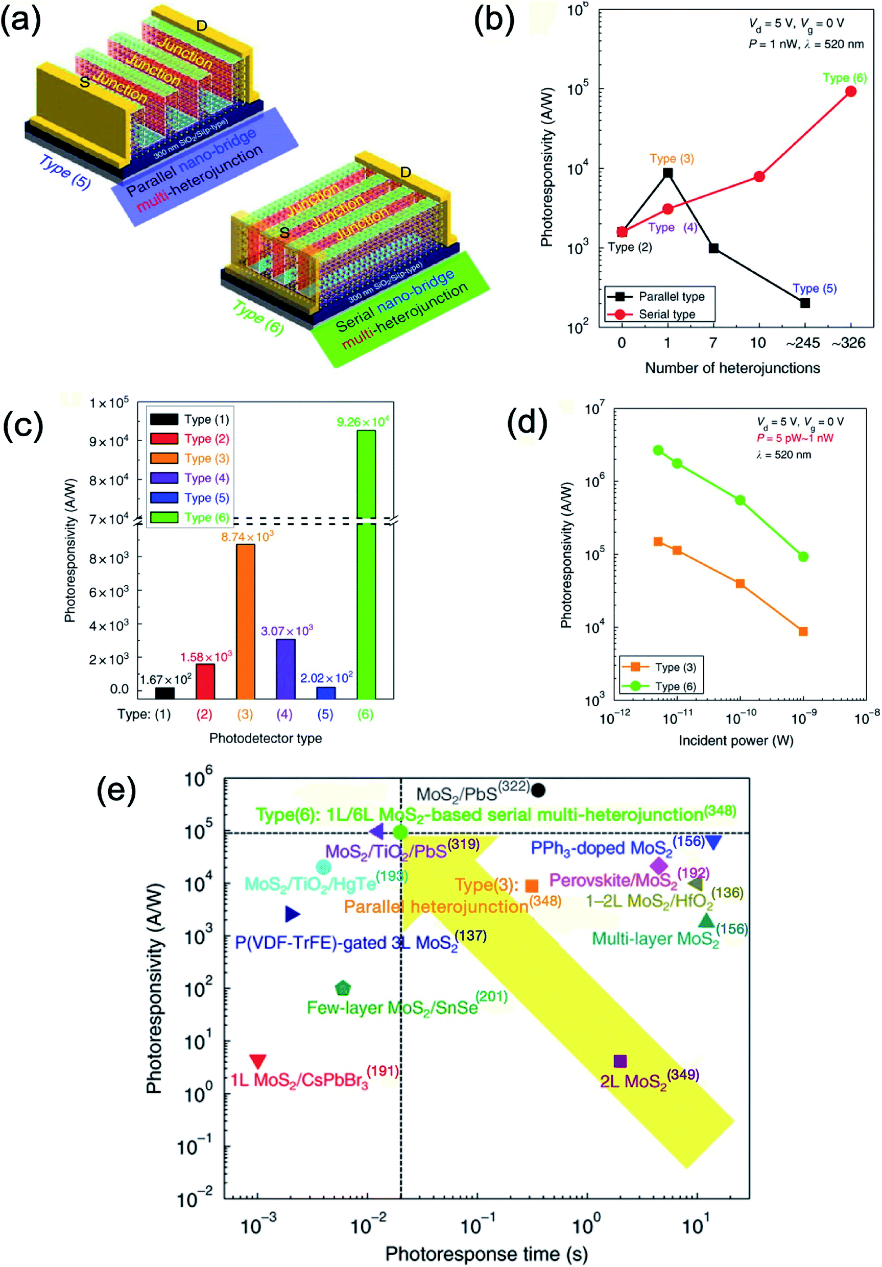 | ||
| Fig. 24 (a) The schematic diagram of MoS2 FETs for parallel nano-bridge multi-heterojunction type (5) and serial nano-bridge multi-heterojunction type (6) photodetectors. (b) Photoresponsivity as a function of the number and direction (parallel and serial) of heterojunctions in the MoS2 channel. (c) The photoresponsivity of type (1) to (6) MoS2 multi-heterojunctions. (d) Photoresponsivity of type (3) and (6) MoS2 photodetectors as a function of the incident laser power at 500 nm. (e) A comparison of photoresponsivity and photoresponse time of parallel multi-heterojunction type (3) and serial multi-heterojunction type (6) based MoS2 photodetectors with previously reported data on MoS2 photodetectors (see ref. 136, 137, 156, 191–193, 201, 319, 322 and 349). Reprinted with permission from ref. 348, copyright © Springer Nature. | ||
The mechanisms of photoconductivity in atomically thin layered MoS2 has been described by Furchi et al.349 Sun et al.350 developed photodetector using multilayer/monolayer MoS2 heterojunction where the source electrodes were connected to the 0.65 nm thick MoS2 monolayer and the drain electrodes were connected with the 6.9 nm thick MoS2 multilayer and the back gate was heavily p-doped Si. The multilayer/monolayer MoS2 heterojunction showed photoresponsivity of 103 A W−1, detectivity of 7 × 10¹⁰ Jones and photosensitivity of 1.7 × 10⁵ at 470 nm. Abnormal photoresponse was noticed under positive gate voltage due to the heterojunction formation. Yan et al.351 fabricated photodetectors using CVD-grown MoS2 bilayer flakes which showed photoresponsivity of 7160 A W−1, detectivity of 6.62 × 10¹⁰ Jones and response/recovery times of 97 ms/291 ms, compared to photoresponsivity of 2900 A W−1 and detectivity of 2.44 × 10¹¹ Jones for the monolayer MoS2 flakes.
5.5 MoS2/inorganic semiconductor heterostructures
Gallium nitride (GaN), a wide-bandgap semiconductor, has been used with MoS2 for developing hybrid photodetectors. The self-powered few-layer MoS2/GaN heterojunction-based deep-ultraviolet (DUV) photodetector was developed by Zhuo et al.316 In order to develop a MoS2/GaN p–n heterojunction photodetector, the MoS2 thin films were transferred onto a GaN substrate where e-beam evaporation method was used to deposit Au electrode on the MoS2 film and Ni/Au electrode on the GaN layer. The MoS2/GaN photodetector exhibited the current Ion/Ioff ratio of 105 at 2.4 mW cm−2 and over 103 at a laser light intensity of 2 μW cm−2, indicating the detection of a weak UV light signal under 265 nm laser illumination at zero bias voltage (0 V) without any external power (self-powered mode). The linear dynamic range (LDR) of 97.3 dB was calculated at zero bias voltage, much better than those of other photodetectors. The rise/fall times were found to be 0.302 ms and 3.605 ms at 100 Hz which further improved at 5 kHz. The MoS2/GaN photodetectors exhibited photoresponsivity of 187 mA W−1, detectivity of 2.34 × 10¹³ Jones, fast response speeds of 46.4 μs/114.1 μs at 5 kHz under a DUV light illumination of 265 nm at 0 V bias. Liu et al.317a fabricated ML MoS2-based phototransistor on a transparent GaN wafer using CVD technique. High quality MoS2/GaN hybrid films were obtained because of the small thermal expansion coefficient (TEC) mismatch and near lattice match between MoS2 and GaN. The photocurrent MoS2/GaN-based FETs was found to be 3–4 times higher at 405 nm compared with 638 nm arising from high absorption and photocurrent gain process. The value of EQE also increased significantly, from 115% at 638 nm to 5289% at 405 nm. The photoresponsivity of 0.59, 2.78, and 17.2 A W−1 was measured at 638, 532, and 405 nm wavelengths under 2 mW laser power, respectively. The response time (trise) decreased from 4.2 s at 638 nm to 0.1 s at 405 nm. MoS2/GaN hybrid-based photodetector showed the maximum photoresponsivity of 17.2 A W−1, EQE of 5289%, and photocurrent gain of 53.6 at 405 nm under incident laser-power of 2 mW using an applied voltage of 9 V. The specific detectivity and the low noise equivalent power (NEP) varied from 6.3 × 10¹⁰ to 1.8 × 10¹² Jones and 2.8 × 10⁻¹² to 9.6 × 10⁻¹⁴ W Hz−1/2 in 405 nm to 638 nm wavelength range, respectively. Li et al.317b demonstrated the improvement of photoresponse of ML MoS2/GaN photodetector by depositing 3 nm thick Al2O3 layer on the surface with ALD method. The photocurrent of Al2O3/MoS2/GaN heterostructure-based photodetector increased more than twice compared to MoS2/GaN device at 365 nm wavelength under applied voltage of 20 V due to the tensile strain enhancement. The Al2O3/MoS2/GaN photodetector showed over two-fold increase in the photoresponsivity, EQE, and photogain than that of MoS2/GaN photodetector where EQE and photogain values increased from 3848% to 8381% and 239 to 520, respectively.Indium selenide (InSe) is a well-known photodetector.352a–d The MoS2 QDs decorated indium selenide (InSe) nanosheets were applied to develop hybrid phototransistors which yielded the photoresponsivity of 9.304 × 10³ A W−1, three orders (103) of magnitude higher than that of InSe photodetector (12.3 A W−1).336 The higher photoresponsivity of hybrid photodetector originated from the MoS2 QDs injected photoexcited carriers to the InSe phototransistor. Ulaganathan et al.353 decorated MoS2 quantum dots (QDs) with InSe nanosheets to develop hybrid phototransistors. The MoS2/InSe-FET showed photoresponsivity of 9304 A W−1 under illumination at 488 nm at source–drain voltage (Vds) = 1 V and gate voltage (Vg) = 0 V, which was 105 times higher compared to InSe based photodetector (0.101 A W−1 at 532 nm) and nearly 10 times higher compared to 2D-graphene/2D-InSe hybrid photodetector (940 A W−1 at 532 nm).352d Here again, the higher photoresponsivity of MoS2/InSe hybrid photodetectors originated due to the transfer of photogenerated charge carriers from MoS2 QDs to the InSe nanosheets. β-In2Se3 is a group IIIA–VIA atomic layered semiconducting material having a small bandgap, which has been used for developing MoS2 hybrid photodetectors. The few layer β-In2Se3 thin films were epitaxially grown on the top of CVD-MoS2 monolayers by Mahapatra et al.354 The β-In2Se3/MoS2 vdW heterostructure-based photodetectors showed significantly higher photoresponse than that of pure β-In2Se3 photodetectors. The photocurrent of In2Se3/MoS2 hybrid-based devices was found to be 1.3 × 10³ times higher compared with the dark current at 532 nm under laser power of 8.47 μW and the EQE value reached 5.49 × 10³% under laser power of 4 mW cm−2 with applied bias.
Silicon355 has been widely used for developing broadband hybrid photodetectors for communication technology. Guo et al.356 used MoS2/Si heterostructure to fabricate a photodetector showing photoresponsivity of 746 mA W−1 and detectivity of 6.03 × 10¹¹ Jones and response/recovery time of 178 μs/198 μs in the 405 to 980 nm range. In another study, multilayer MoS2 films were deposited on Si quantum dots (Si QDs) to develop heterojunction photodetectors which showed much faster response/recovery time of 60 ns/756 ns and detectivity of 6.1 × 10¹³ Jones.357 Au nanostructure-based plasmonic-enhanced multilayer MoS2 photodetector deposited on p-type Si substrate exhibited photoresponsivity of ∼37 A W−1 and detectivity of ∼1012 Jones in 405–780 nm wavelength range.358 The photoresponsivity of the Au plasmonic-enhanced MoS2/Si photodetector was enhanced by 8.0, 5.3 and 11 times at 405 nm, 650 nm and 780 nm under 5 V bias, respectively, compared to the pristine p-Si photodetector. The Au plasmonic-enhanced MoS2/Si photodetector also displayed a fast response time of 1 μs and a recovery time of 18 μs.
The 2D MoS2/1D ZnO heterostructure-based photodetectors have been developed to increase the light absorption range and photoresponsivity.360 The dark current of p-MoS2/n-ZnO heterostructure was measured as 0.88 nA which increased significantly to 103.1 nA and 2.52 nA at 365 nm (light intensity of 112 mW cm−2) and 532 nm (64 mW cm−2) under +5 V of applied voltage, respectively, demonstrating high sensitivity to UV and visible illuminations. The current Ion/Ioff ratio was found to be 109 at 365 nm and 3.3 at 532 nm. The n-MoS2/n-ZnO photodetectors showed the photocurrents of 33.6 nA to 88.2 nA and 0.3 nA to 1.86 nA at 365 nm (5.7 to 47.2 mW cm−2) and at 532 nm (0.525 to 56.7 mW cm−2), respectively. The p-MoS2/n-ZnO photodetectors showed photoresponsivity of 24.36 A W−1 and EQE of 8.28 × 10³% under 365 nm light illumination.
Semimetal cadmium arsenide (Cd3As2) has been used for fabricating broadband photodetectors due to its higher mobility as well as high absorption of light in a broad spectral region.361 Cd3As2 nanoplates have been integrated with multilayer MoS2 to develop a heterojunction photodetector which yielded high photoresponsivity of 2.7 × 10³ A W−1 at room temperature.362 Likely, CdSe nanoplates were vertically assembled on MoS2 monolayer to develop vertical CdSe/MoS2 heterostructures.363 CdSe/MoS2 heterostructure-based photodetector exhibited photoresponsivity of 1.63 A W−1 and fast response speed of 370 μs. In another study, 2D MoS2 nanosheet and 0D CdSe nanocrystal-based hybrid phototransistor were developed which showed substantially enhanced photoresponsivity of 2.5 × 10⁵ A W−1 and the rise/fall times of 60 ms.323 The photocurrent of MoS2/CdSe hybrid photodetector increased with increasing laser power intensities at 405 nm. Ghosh et al.364 developed photodetectors using a nanocomposite of single flake MoS2 and lanthanide doped upconversion nanoparticles (UCNPs). The MoS2/UCNPs based photodetector showed highest photoresponsivity of 1254 A W−1, detectivity of 1.05 × 10¹⁵ Jones and a gain of 7.12 × 10⁻⁴ cm2 V−1 at 980 nm for 1.0 V bias. The highest detectivity of 9.0 × 10¹³ Jones at 405 nm and the lowest detectivity of 3.4 × 10¹³ Jones at 808 nm was observed for MoS2/UCNPs devices. Likely, MoS2/UCNPs photodetectors showed the highest normalized gain (Γn) of 1.48 × 10⁻⁴ cm2 V−1 at 405 nm and the lowest Γn of 2.8 × 10⁻⁵ cm2 V−1 at 808 nm laser wavelength, which is an order of magnitude higher compared with those reported for MoS2 monolayer (Γn = 4.8 × 10⁻⁶ cm2 V−1).171 Multilayer MoS2 films on monocrystalline SiC substrate using CVD were deposited by Xiao et al.365 MoS2/SiC hybrid photodetector showed photoresponsivity of 5.7 A W−1 at 365 nm under 4.35 μW incident light power. Instead of Si, Wu et al.366 used Si nanowire arrays (SiNWA) with few-layer MoS2 films to enhanced light absorption region of photodetectors. The dark current of the MoS2/SiNWA photodetector was found to be much lower compared with MoS2/bulk Si photodetector; contrary to this, the photocurrent of the MoS2/SiNWA photodetectors was much increased than that of the MoS2/bulk Si photodetector due to the increased light absorption and contact area between MoS2 and Si. The Ion/Ioff current ratio of MoS2/SiNWA photodetectors varied from 3.2 × 10² to 1.1 × 10⁵ as the light intensity changed from 0.031 mW cm−2 to 32 mW cm−2 under zero bias at 650 nm. The MoS2/SiNWA heterojunction-based photodetector showed photoresponsivity of 53.5 A W−1, and detectivity of 2.8 × 10¹³ Jones under laser power intensity of 6.3 μW cm−2, much higher than that of MoS2/bulk Si photodetector.311–313 The rise/fall times of photodetectors was found to decrease with increasing light intensity where the rise times varied from 54.2, 27.7, 23.5 to 22.8 μs, and fall times from 69.9, 68.6, 67.4 to 61.5 μs under laser power intensity of 2.5, 16.8, 24.5 and 38.6 mW cm−2, respectively.
Organic/inorganic hybrid halide perovskite (C6H5C2H4NH3)2PbI4 = (PEA)2PbI4 with ML MoS2 has been used to develop hybrid photodetectors by Wang et al.367 (PEA)2PbI4 functions as an electron reservoir to decrease free charge carriers as well as a to passivate defects. The dark current was reduced by six orders of magnitude by depositing (PEA)2PbI4 thin film over MoS2 photodetector due to the charge transfer from ML MoS2 to (PEA)2PbI4 thin film. The use of (PEA)2PbI4 over ML MoS2 reduced the charge carrier density which yielded a broadband photodetector (200 to 900 nm) exhibiting photoresponsivity of 16.8 A W−1, detectivity of 1.06 × 10¹³ Jones, EQE of 3.3 × 10³ and on/off ratio of 105. The photoresponse speed of a hybrid photodetector was enhanced over 100-times that of a pristine MoS2 photodetector due to (PEA)2PbI4 passivation. (PEA)2PbI4/MoS2 hybrid photodetectors also work at 0 V bias, which is a self-powered mode where photocurrent showed an increase with increasing laser power intensity from 2.8 nW to 109.8 nW and the rise/decay times of 38 ms/24 ms under 637 nm laser wavelength. Shen et al.368 synthesized a series of helicene 5,14-diaryldiindeno[2,1-f:1′,2′-j]picene (DDP) derivatives namely 5,14-dimesityldiindeno[2,1-f:1′,2′-j]picene (1ab), 5,14-bis(2,4,6-trimethoxyphenyl)diindeno[2,1-f:1′,2′-j]picene (1ac), and 9,10-dimethyl-5,14-dimesityldiindeno[2,1-f:1′,2′-j]picene (1bb) and integrated with monolayer MoS2 to develop hybrid photodetectors. Time-resolved measurements showed the interfacial charge-transfer from the DDP derivative to the monolayer MoS2 confirmed by the stability of exciton property of the (1ac)/MoS2 organics/inorganic hybrid heterostructure. The 1ac/MoS2 hybrid based photodetector showed high photoresponsivity of 4.99 × 10⁷ A W−1 and response time of 45 ms at 633 nm using laser light intensity of 5.75 nW under Vd = 5 V and Vg = 0 V because of the efficient separation of photoexcited carriers and the alignment of type-II energy band. The photoresponsivity of the organic/inorganic hybrid photodetectors followed the sequence of (1ac)/MoS2 > (1ab)/MoS2 > (1bb)/MoS2 as a function of light intensity and after storing for one month. Furthermore, 1ac/MoS2 hybrid photodetector did not exhibit any degradation after one-month storage. MoS2 hybrid heterostructure-based photodetectors have been mainly studied having a type II band alignment.
The MoS2 atomic layers were also prepared by different methods. Kumar et al.369 developed large-area MoS2 layers using pulsed laser deposition (PLD) method which showed photoresponsivity of 3 × 10⁴ A W−1 and detectivity of 1.81 × 10¹⁴ Jones at 365 nm under 24 μW cm−2 incident light power at applied bias of 2.0 V. The photoresponsivity of the PLD-grown few-layer MoS2 photodetectors was found to be 3 × 10⁴, 1.08 × 10⁴, 7.0 × 10³, and 6.3 × 10³ A W−1 at 365, 436, 546, and 655 nm wavelengths under applied bias of 2 V, respectively. FL-MoS2 photodetectors also showed low dark current of 10−10 A and photoresponse of 1.37 × 10⁵. Schneider et al.370 used metalorganic vapor-phase epitaxy (MOVPE) method to develop FL MoS2 based flexible photodetectors. The photoresponsivity and specific detectivity of MoS2 photodetectors can be changed between 150 A W−1 to 920 A W−1 and 1012 Jones to 1010 Jones by using electrostatic gating, respectively.
Singh et al.371 reported Pd/Al2O3/MoS2/ITO photodetector showing photoresponsivity of 488 A W−1, detectivity of 8.22 × 10¹² Jones and EQE of 1.9 × 10⁵% at 308 nm wavelength under laser light intensity of 13.6 μW/cm2 with 1 V applied bias voltage. Ye et al.372 demonstrated vertical growth of Sb2O3 flakes on monolayer MoS2 crystals by using CVD technique. The Sb2O3 flakes of different thickness and size covered monolayer MoS2 crystals in 10, 21, 44, 54 and 100% ratio and their based back-gated FETs fabricated on SiO2/Si wafer affected the carrier mobility and subthreshold swing (SS) of the Sb2O3/MoS2 hybrid photodetectors. The photocurrent, photoresponsivity, detectivity, sensitivity and EQE of hybrid FETs were measured as a function of laser power intensity under 360, 457, 532, 671, 914, and 1064 nm light illuminations. The hybrid FET-21% exhibited photocurrents of 263 and 2.5 μA at laser power intensities of 177 and 11 mW cm−2 under 360 and 1064 nm laser illuminations, respectively. The photoresponsivity of 5.3 × 10⁴ A W−1 and detectivity of 2.0 × 10¹⁵ Jones were measured at 457 nm wavelength whereas in the NIR region, Sb2O3/MoS2 hybrid photodetectors showed photoresponsivity of 7.8 A W−1, detectivity of 3.4 × 10¹¹ Jones, and response speed of <60 ms with 1064 nm laser wavelength at room temperature. Sb2O3/MoS2 hybrid photodetectors (FET-21%) showed photoresponsivity of 1.1 × 10⁴ A W−1 and detectivity of 4.5 × 10¹⁴ Jones under 360 nm laser wavelength. The hybrid FET-21% also showed sensitivity values of 6 × 10², 2.5 × 10³, 3 × 10³, 2.4 × 10³, 0.2, and 0.5 cm2 W−1 and EQE values of 4.0 × 10⁶, 1.4 × 10⁴, 1.0 × 10⁴, and 5.5 × 10³, 0.4, and 0.9% under laser illuminations of 360, 457, 532, 671, 914, and 1064 nm, respectively. Higher photoresponse has been observed in 2D metal NiTe2 and semiconductor MoS2 heterostructure-based back-gated FETs and photodetectors compared to a pristine MoS2 monolayer.373 As discussed earlier, that the MoS2 vdWH-based photodetectors show great promise for pratical applications, therefore, new vdW heterostructures have been targetted. The NiTe2/MoS2 vdW heterostructure-based photodetectors showed several times faster rise/decay times than that of a MoS2 photodetector due to the epitaxial grown metallic vdWHs. Photodetectors were also developed from the WSe2 and MoS2 vdWHs where MoS2 was used as a channel in the phototransistor.374 The MoS2 vdWH-based phototransistor showed high photoresponsivity of 2700 A W−1, detectivity of 5 × 10¹¹ Jones, and response speed of 17 ms. In these phototransistors, the vertical built-in electric field in the WSe2–MoS2 p–n junction separated the photoexcited charge carriers, which yielded a photoconductive gain of 106. Ying et al.375 fabricated BaTiO3/MoS2 heterostructure-based photodetectors with type I band alignment which showed photoresponsivity of 120 A W−1 and EQE of 4.78 × 10⁴% compared with 1.7 A W−1 and 4.5 × 10²% for the bare MoS2 at 365 nm under low laser power intensity of 0.095 mW cm−2. Both micro-Raman spectroscopy and photoluminescence indicated the occurrence of carrier extraction and carrier injection processes in the MoS2 layer, leading to the boosting of the number of carriers in the MoS2 channel. The high performance of type-I hybrid heterostructure-based photodetectors originated from the carrier extraction process between BaTiO3 NPs and MoS2 layer.
5.6 MoS2 nanoscrolls
MoS2 nanoscrolls have been prepared by argon plasma treatment of monolayer MoS2 nanosheet where the MoS2 nanoscroll formation also results in a partial removal of sulfur atoms from the top sulfur layer in MoS2.376 The luminescent MoS2 nanoscrolls have also been prepared by the supercritical fluid processing method. The exfoliated MoS2 nanoscrolls showed photoluminescence from 420 to 600 nm due to the size reduction and polydispersity.377 The 1D MoS2 nanoscrolls have been prepared from CVD-grown triangular MoS2 nanosheets where the formation of a MoS2 nanoscroll takes place from the edge of a triangular nanosheet along the armchair orientation of MoS2.378 The carrier mobility as well as physical contact properties of 1D MoS2 nanoscroll-based FETs were found to be quite different than that of 2D MoS2 nanosheets. The 2D semiconductor MoS2 nanosheets can be transformed into 1D metallic MoS2 nanoscrolls. This demonstrated that 1D TMD-based nanoscrolls with unique chemical, physical and electrical properties can be fabricated.The photodetectors fabricated using MoS2 or WS2 nanoscroll were compared with monolayer MoS2 or WS2 photodetectors.379 MoS2 or WS2 nanoscroll-based devices showed photosensitivity enhancement by two orders of magnitude, demonstrating the potential of 2D TMD-based 1D nanoscrolls in optoelectronic applications. 1D MoS2 and WS2 nanoscroll-based photodetectors exhibited very high photocurrent-to-dark-current ratio compared with 2D nanosheet-based photodetectors. Deng et al.380 prepared MoS2 nanoscroll-based photodetectors using the avalanche multiplication effect where a low triggering electrical field is required than that of MoS2 atomic layers. Fig. 25(a–c) shows schematic illustration of MoS2 nanoscroll-based avalanche photodetectors having MoS2 nanoscroll channel (area of 1.8 μm2) connected with source and drain metal electrodes, photoresponsivity and detectivity as a function of applied bias voltage (Vds) under 532 nm laser illumination. Self-assembled MoS2 nanoscrolls were prepared using ethanol droplet and by rolling the monolayer MoS2 flake. The doped silicon film was used as the substrate as well as a gate electrode. A MoS2 nanoscroll is formed under strain compared with a monolayer MoS2 flake, therefore, an analysis of the MoS2 bandgap was carried out under applied tensile strain. As the uniaxial tensile strain was increased from 0% to 3% for the monolayer MoS2 flake, the bandgap of MoS2 decreased from 1.77 to 1.5 eV, associated to a decrease in avalanche critical electric field (Eava) in MoS2 nanoscrolls. The avalanche multiplication effect was noticed in MoS2 nanoscrolls which also showed high multiplication factor and impact ionization coefficient. The excess noise factor was measured as a function of the multiplication factor. The multiplication factor of 40 was recorded at Vds of 45 V which depended on the applied electric field. The avalanche gain of 24 was also measured at Vds = 45 V for the MoS2 nanoscroll-based devices. The electrical field (Eava) to trigger avalanche multiplication in MoS2 nanoscrolls was found to be dramatically decreased compared with monolayer MoS2 flakes. The decrease of Eava in MoS2 nanoscrolls was associated with several factors including reduced bandgap, substrate contacts and phonons suppressed scattering of the free carriers. The decrease in bandgap of MoS2 nanoscroll was also evidenced by a red-shift compared with the monolayer MoS2 flake. MoS2 nanoscroll-based photodetectors exhibiting photoresponsivity over 104 A W−1, detectivity of 2 × 10¹² Jones and 30 times higher avalanche gain compared with monolayer MoS2 flake. This study showed low-power consumption MoS2 nanoscroll-based photodetections where avalanche multiplication effect enhanced the photoresponsivity in MoS2 nanoscrolls compared with atomically thin monolayer MoS2. Deng et al.381 reported photodiodes having p-type WSe2 and single MoS2 nanoscrolls which showed suppressed dark current and two orders of magnitude increase in the ratio of photocurrent to dark current compared with a single MoS2 nanoscroll-based photodiode. Fig. 25(d–f) shows schematic illustration of the WSe2/MoS2 nanoscroll-based photodiode, incident power intensity dependent current Ion/Ioff ratio of single MoS2 nanoscroll and WSe2/MoS2 nanoscroll-based heterojunction and photoresponsivity of the WSe2/MoS2 nanoscroll-based hybrid photodetector as a function of incident power intensity. The response speed of WSe2/MoS2 nanoscroll-based device increased by three orders of magnitude than that of a single MoS2 nanoscroll device. The WSe2/MoS2 nanoscroll-based photodetectors exhibited the photoresponsivity of 0.3 A W−1, EQE values of 25% at zero bias voltage and 75% at a reverse bias of 1 V at 532 nm under laser power intensity of 1.14 mW cm−2 and response speed of 5 ms with laser power intensity of 60 mW cm−2. The atomic layered WSe2/MoS2 nanoscrolls were found to be superior to those of MoS2 nanoscrolls. Wang et al.382 developed WS2/MoS2 vdWH-based nanoscrolls by dropping aqueous alkaline droplets on CVD-grown BL WS2/MoS2 vdW hybrid heterostructure, which were prepared by growing 1L WS2 islands on top of 1LMoS2 nanosheets. The optical microscopy, AFM, ultralow frequency (ULF) Raman spectroscopy and TEM techniques were used to characterize the WS2/MoS2 vdWH-based nanoscrolls and ULF breathing and shear mode peaks were observed which originated from the strong interlayer interaction. The photosensitivity of WS2/MoS2 nanoscroll-based photodetectors were found to be ten times higher compared withWS2/MoS2 vdWH-based photodetectors under blue, green and red laser illuminating lights; the ultrafast charge transfer process occurring in nanoscrolled structure at alternative WS2/MoS2 and MoS2/WS2 multi-interfaces could be associated with such a high performance.
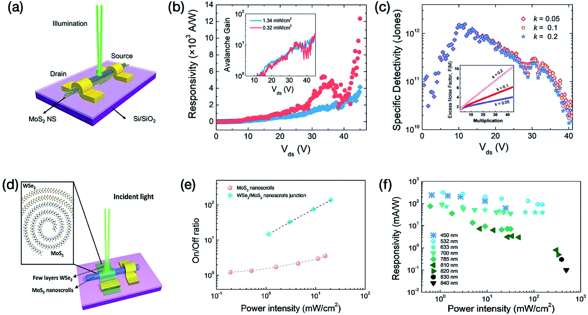 | ||
| Fig. 25 (a) Schematic illustration of MoS2 nanoscroll-based avalanche photodetector under illumination. (b) Photoresponsivity of the avalanche photodetector as a function of applied bias voltage (Vds) under 532 nm laser illumination at different incident light power intensities. Inset shows the Vds dependent avalanche gain. (c) Specific detectivity of the avalanche photodetector as a function of Vds. The inset is a plot of excess noise factor as a function of the multiplication factor. Reprinted with permission from ref. 380, copyright © American Chemical Society. (d) Schematic illustration of the WSe2/MoS2 nanoscroll-based photodiode along with the cross-section of the heterojunction containing MoS2 nanoscrolls and few layers WSe2 where electrodes are source and drain, respectively. (e) The current Ion/Ioff ratio of single MoS2 nanoscroll and WSe2/MoS2 nanoscroll-based heterojunction as a function of incident power intensity at 532 nm wavelength. (f) Photoresponsivity of the WSe2/MoS2 nanoscroll-based hybrid photodetectors as a function of incident laser power intensity at different wavelengths, showing broadband photodetection by the hybrid heterostructure photodiode. Reprinted with permission from ref. 381, copyright © Wiley. | ||
The research data collected on the figure-of-merit of MoS2 based photodetectors have been extensively documented. Tremendous interest is growing in the field of MoS2 based photodetectors as new research ideas are emerging on a rapid pace.383–387 Ahmed et al.388 fabricated graphene/h-BN/MoS2 trilayer vdW heterostructure-based phototransistors to examine the photogating mechanism where h-BN layer was used as an interfacial barrier to monitor the charge transfer process. Mechanically exfoliated monolayer graphene, MoS2 and multilayer h-BN were used to fabricate the graphene/h-BN/MoS2 vdW heterostructures on the SiO2/(p++)-Si substrate. All optoelectronic measurements were conducted at 180 K temperature under the high vacuum conditions. The incident power density dependent photoresponsivity, NEP and detectivity of vdW heterostructure-based photodetectors were measured from 640 nm to 1720 nm wavelength region. Fig. 26 shows the figure of merit of the graphene/h-BN/MoS2 vdW heterostructure-based photodetectors. The photoresponsivity values of 5 × 10⁹ A W−1 in the visible region, 2 × 10⁹ A W−1 at 940 nm, 108 A W−1 at 1550 nm and 2 × 10⁷ A W−1 at 1720 nm were observed using source drain bias of 20 mV at low power density. The low NEP value of 2 × 10⁻²⁰ W Hz−1/2 at 940 nm was found to be further increased to 2 × 10⁻¹⁸ W Hz−1/2 for 1720 nm. Being correlated to NEP, the high detectivity values of 1016 Jones at 640 nm, 5 × 10¹⁵ Jones at 940 nm and 5 × 10¹³ Jones at 1720 nm were deduced for the vdW hybrid photodetectors, which are two orders of magnitude higher compared to graphene-based IR photodetectors. The values of photoresponsivity, NEP and detectivity for vdWHs differ by several orders of magnitude as a function of laser power density at different measurement wavelengths. This study demonstrated that the defect states can strongly affect to the photoresponse of the graphene/h-BN/MoS2 hybrid photodetectors. The strong photoresponse has been observed in MoS2 atomic layers when integrated with other vdW nanomaterials. As summarized in Table 1 and documented throughout this article, MoS2-based photodetectors show photoresponsivity raging from mA W−1 to 1010 A W−1, detectivity from 107 to 1015 Jones and ultra-fast response speed up to nanoseconds (10−9 s), which varies by several orders of magnitude over an ultra-broadband spectral range from 265 nm to 10 μm under different incident power densities. The performance of MoS2 photodetectors is derived from the design of MoS2 based phototransistors, photoconductors and photodiodes. Several different mechanisms including photoconductive, photovoltaic, photobolometric and surface plasma-wave enhanced effects contribute to the performance of MoS2 photodetectors. Abraham and Majumdar389 analyzed the benchmarking and characterization protocol for photodetectors developed using various types of nanomaterials and pointed out that NEP is one of the most important sensitivity parameters for the figure of merit compared to the photoresponsivity and detectivity. The measurements of NEP as a function of modulation frequency of a photodetector could be used for a better comparison of the figure of merit of heterogeneous photodetectors. The photoresponsivity (R) data were plotted as a function of modulation frequency (f) and NEP for a wide variety of nanomaterial-based photodetectors. Photodetectors with vertical current transport were found to perform much better than photodetectors having lateral current transport as a function of modulation frequency with an exception of graphene-based photodetectors, which is associated with high carrier mobility. However, the measurements of photoresponsivity of these nanomaterials significantly vary depending upon the applied bias voltage and different intensity of laser power; therefore, an accurate comparison is rather convoluted. In the photoresponsivity versus NEP plot, the MoS2-based photodetectors such as monolayer MoS2 phototransistors,171 vertical MoS2 p–n junction,346 MoS2/PbS,322 graphene/WS2/MoS2,347 etc., are in par with PbS-based photodetectors.390 The plot of photoresponsivity versus NEP does not show an important correlation between these two parameters and the higher values of photoresponsivity does not inevitably lead to high sensitivity of photodetectors. High sensitivity of a photodetector can be achieved with a relatively low photoresponsivity by controlling the noise of photodetectors.
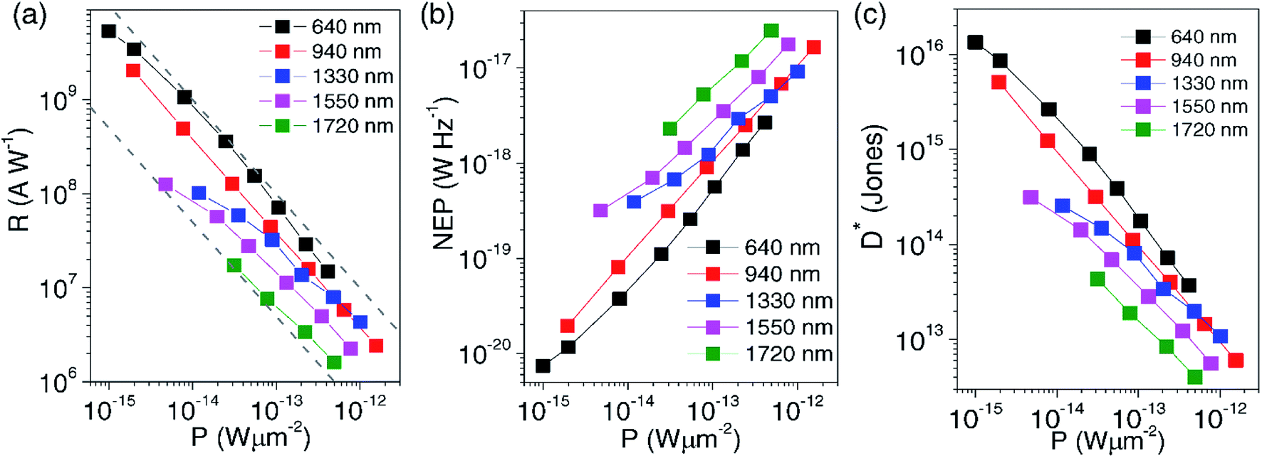 | ||
| Fig. 26 Figure of merit of the graphene/h-BN/MoS2 vdW heterostructure-based photodetectors. Plots of (a) photoresponsivity (R), (b) noise equivalent power (NEP) and (c) specific detectivity (D*) as a function of incident power density (P) in the 640 nm to 1720 nm wavelength region. Reprinted with permission from ref. 388, copyright © Institute of Physics Publishing. | ||
6. Strain-induced and self-powered MoS2 photodetectors
Energy harvesting from piezoelectric materials such as ceramics, single crystals, organic polymers and their based hybrid composites has been investigated over many decades. The commonly known piezoelectric materials include lead zirconate titanate (PZT), barium titanate (BaTiO3), lithium niobate (LiNbO3), zinc oxide (ZnO), quartz, polyvinylidene difluoride (PVDF), poly(vinylidene fluoride-trifluoroethylene) (VPF-TrFE), nylons, liquid crystal polymers, biomaterials, etc.391–398 The piezoelectric, pyroelectric and ferroelectric materials offer capabilities of generating usable energy under applied mechanical strain, temperature, electric field, water, light, etc. therefore, have been integrated in energy harvesting devices for their applications in self-powering footwears, speakers and headphones, motors, batteries, sensors, actuators, catalysis, photovoltaics, optical memory devices, spintronics, robotics, triboluminescence, etc.399–402 In addition to silicon, Ge, SiC, ZnO, TiO2, cement, polymers, diamond, and carbon nanotubes, the piezoresistive effects have been studied in 2D nanomaterials403–410 for applications in piezoresistive strain/stress sensors. Black phosphorus (BP) has been used with MoS2 to develop BP/MoS2 vdW heterostructure-based photodetectors with a type-II band alignment.404 The strain induced piezoelectric effect was observed in BP and MoS2 vdW heterostructures.Piezoelectric and pyroelectric generators have been developed using different types of inorganic and organic materials for their applications in optoelectronic and photonic devices. Kim et al.411 reported piezoelectric effect in CVD-grown monolayer MoS2 films and fabricated direction-dependent flexible piezoelectric nanogenerators where the atomic orientation in monolayer MoS2 dictated the magnitude of the piezoelectric effect. The output power of nanogenerators (NG) was found to be two times higher for the armchair direction of MoS2 compared with zigzag direction of MoS2 under the same applied strain and the strain velocity. The armchair MoS2 showed piezoelectric coefficient d11 of 3.78 pm V−1 whereas the zigzag MoS2 exhibited much lower d11 value of 1.38 pm V−1. The armchair MoS2 nanogenerator exhibited higher output voltage of 20 mV as well as the higher output current of 30 pA than that of 10 mV and 20 pA for the zigzag MoS2 nanogenerator, confirming the role of atomic orientation in enhancing piezoelectric effect in 1L MoS2 nanogenerators. Tsai et al.412 reported piezoresistive effect in flexible MoS2 FETs which was associated with the strain-induced bandgap change as confirmed using optical reflection spectroscopy. The bandgap of the 3L MoS2 was found to decrease by 0.0 6 eV (from 1.58 eV to 1.52 eV) under 0.2% applied strain. The effects of both piezoelectricity and piezoresistivity on photoresponse of atomic layered MoS2 have been studied.
Strain-induced photodetection has been observed in MoS2 atomic layers and MoS2 based hybrid heterostructures. The monolayer MoS2 based photodetector showed photoresponsivity of 2.3 × 10⁴ A W−1 under a compressive strain of −0.38% at low laser power intensity of 3.4 μW cm−2 with 442 nm wavelength.264 Gas sensitivity has been reported in 1L MoS2 via photogating and piezo-phototronic effects.413 Monolayer MoS2 based flexible homogenous photodiode showed 619% and 319% enhancement in photoresponsivity and detectivity after applying 0.51% tensile strain, where the photoresponsivity and detectivity reached maximum values of 1162 A W−1 and 1.72 × 10¹² Jones, respectively, compared with a strain-free photodiode.414 The in-plane anisotropic photoresponse has been reported in monolayer MoS2.415 The crystal symmetry of monolayer MoS2 was found to be reduced from D3h to C2v under applied uniaxial tensile strain. The absorption along the armchair direction of monolayer MoS2 was found to be two times higher compared to zigzag direction under 4.5% strain, which also increased with increasing strain, whereas the absorption along zigzag direction of monolayer MoS2 showed a slight change. The photoresponse of monolayer MoS2 changed from isotropic to anisotropic at 520 nm light illumination. The photoresponse was not observed in monolayer MoS2 devices until uniaxial tensile strain reached to a value of 3.5% and the anisotropic ratio higher than 2 was recorded under 4.5% uniaxial tensile strain at 520 nm and 830 nm wavelengths.
In another study, the photoresponsivity of flexible MoS2/WSe2 heterojunction-based photodiodes increased by 86% under a static strain of −0.62% when applied along the armchair direction of MoS2 due to the piezoelectric effect.416 Similar strain-induced photoresponse has been measured in MoS2 and ZnO p–n heterojunction photodiodes where photocurrent increased over four times under an applied pressure of 23 MPa.417 The photoresponsivity of ML MoS2/GaN heterojunction photodiodes was also inhanced by 3.5 times under 258 MPa applied pressure originating from strain-induced piezoelectric phenomenon.418
The effect of piezoresistivity on performance of MoS2 photodetectors has also been studied. Li et al.419 reported piezoelectric and piezoresistive effects in a flexible CVD-grown monolayer MoS2/polyethylene naphthalate (PEN) substrate-based photodetector. An enhancement of photoresponse such as light–dark current ratio from 29 to 1200.3 (41 times) at 1 V bias voltage and self-powered current from 25.2 to 213.6 pA (8.3 times) was observed in armchair direction monolayer MoS2 after applying 0.8% strain due to the piezoelectric effect. However, the photoresponsivity decreased from 163.9 to 95.7 A W−1 under 0.8% applied strain at 5 V bias voltage. The photocurrent increased from 0.37 to 2.35 μA and photoresponsivity from 114.3 to W to 590 A W−1 in zigzag direction monolayer MoS2 under 1.4% applied strain at 5 V due to the piezoresistive effect. The zigzag direction monolayer MoS2 showed no piezoelectric effect. Kelvin probe force microscopy was used to analyze both piezoelectric and piezoresistive effects in monolayer MoS2. Gant et al.420 reported strain-induced increase in both photocurrent and photoresponsivity of flexible monolayer MoS2 photodetectors. The monolayer MoS2 based photodetector showed significant increase in photocurrent at 740 nm light illumination under incident power density of 5 mW cm−2 with 5 V applied bias voltage when tensile biaxial strain was increased from 0.16% to 0.48%. In biaxially strained polycarbonate substrate-based flexible MoS2 photodetectors, the photoresponsivity increased 100 and 1000 times by increasing applied strains from −0.8% to 0.48% and from −1.44% to 0.48%, respectively.
2D material-based self-powered heterojunction photodetectors are also gaining much attention because no external power is required for the photodetection.421 The self-powered p-MoTe2/n-MoS2 vdWH-based photodetector having ITO electrodes showed photoresponsivity of 146 mA W−1 and fast photoresponse of ∼172 μs from 450 nm to 980 nm.422 The photodetector also exhibited bidirectional photocurrent response associated with type-II band aligned heterostructure and ITO electrodes. Yang et al.423 used narrow bandgap layered semiconductor germanium selenide (GeSe) for developing hybrid photodetectors where photoconductive GeSe/graphene photodetectors were compared with photovoltaic GeSe/MoS2 photodetectors. The photodetector based GeSe/graphene vdWHs showed higher photoresponsivity up to 104 A W−1 under laser light intensity of 0.17 mW cm−2 at 532 nm whereas the GeSe/MoS2 heterostructure based photodetector exhibited low photoresponsivity of 0.1 A W−1 but a faster recovery time of 5 ms compared with 2 s for GeSe/graphene heterostructure. GeSe/MoS2 photodetector retained constant photoresponse under applied reverse bias because of the reduced carrier conduction within depletion region. Xin et al.424 fabricated polarization-sensitive self-powered photodetectors using type-II band aligned GeSe/MoS2 vdWHs to increase photoresponse spectrum and support efficient separation as well as transportation of the photoexcited charge carriers. GeSe/MoS2 p–n heterojunctions were developed using mechanically exfoliated GeSe and MoS2 nanoflakes on p-doped Si substrate having a SiO2 film of 300 nm thickness. Fig. 27(a–c) shows a type-II band aligned GeSe/MoS2 p–n hetero-junction photodetector with Ti/Au electrodes, and time-dependent photoresponse at different illumination wavelengths (UV-NIR region), and photoresponsivity and detectivity of the self-powered GeSe/MoS2 heterojunction photodetectors as a function of wavelength from 380 to 1064 nm at Vds of 0 V (zero bias). The self-powered GeSe/MoS2 photodetector achieved Ion/Ioff current ratio of 104 at zero bias, photoresponsivity of 105 mA W−1 and EQE of 24.2%. GeSe/MoS2 vdWH-based photodetectors showed photoresponse from 380 to 1064 nm and showed maximum photoresponsivity of 590 mA W−1 at 532 nm wavelength. The photoresponsivity of the self-powered GeSe/MoS2 p–n heterojunction photodetector varied from 6.1 mA W−1 to 150 mA W−1 while the detectivity remained at 1011 Jones in the 380 nm to 1064 nm (UV-NIR) range. Photoresponse was also measured as a function of polarization angle from 0° to 360° where the current on/off ratios were found to be 7.23 × 10³, 3.65 × 10⁴, and 2.99 × 10³ at 30°, 90° and 120° polarization angles under 532 nm light illumination with Vds of 0 V, respectively. The highest photocurrent of −3.08 × 10⁻¹⁰ A was recorded at 90° and 270° polarization angles corresponding to the armchair direction of GeSe which was also a parallel direction of the polarization, whereas the lowest photocurrent of −1.04 × 10⁻¹⁰ A was measured at 0° and 180° polarization angles which corresponded to the zigzag direction of GeSe. The polarization-sensitive photodetection in the self-powered GeSe/MoS2 photodetector was observed due to the absorption and anisotropic electronic transport associated with GeSe nanoflakes.
 | ||
| Fig. 27 (a) Schematic illustration of a type-II band aligned GeSe/MoS2 p–n heterojunction photodetector having Ti/Au electrodes, separation of the photoexcited electrons–holes carriers and energy band diagram under 532 nm light illumination at Vds of 0 V (zero bias). (b) Time-dependent photoresponse of the heterojunction photodetector under different illumination wavelengths at Vds = 0 V. (c) Photoresponsivity and detectivity of the GeSe/MoS2 heterojunction photodetectors as a function of wavelength. Reprinted with permission from ref. 424, copyright © American Chemical Society. (d) Schematic illustration of a self-powered MoS2 photodetector based on p–i–n-type perovskite photodiode/solar cell bifunctional (PPSB) device consisting of Al/BCP/PCBM/MAPbI3/MoS2/co-GR; where BCP = bathocuproine, PCBM = phenyl-C61-butyric acid methyl ester, MAPbI3 = methylammonium lead tri-iodide perovskite, co-GR = graphene electrode co-doped with AuNPs and (trifluoromethanesulfonyl)-amide. MoS2 based flexible PPSB photodetector was fabricated using a PET substrate. (e) Current Ion/Ioff switching behavior of flexible PPSB photodetectors at 500 nm at 0 V bias. (f) Wavelength-dependent photoresponsivity and detectivity of flexible photodetector recorded at 0 V bias, therefore in a self-powered mode. Inset is an optical image of a flexible self-powered PPSB photodetector. Reprinted with permission from ref. 425, copyright © Elsevier; (g) schematic illustration of CZTS/MoS2 p–n heterojunction-based photodetector and current–voltage (I–V) curves in the dark and at different laser wavelengths (400 nm to 1100 nm) under illumination. (h) Curve of photoresponsivity as a function of wavelength and (i) calculated rise/decay times of the self-powered CZTS/MoS2 photodetector from 400 nm to 1100 nm wavelengths. Reprinted with permission from ref. 428, copyright © Elsevier. | ||
The perovskites have been used with MoS2 to develop organic/inorganic hybrid-based photodiode–solar cell bifunctional devices. Shin et al.425 used MoS2 as a hole transport layer (HTL) and graphene (GR) co-doped with AuNPs and (trifluoromethanesulfonyl)-amide (co-GR) as transparent conductive electrodes (TCE) to develop flexible p–i–n-type perovskite-based photodiode/solar cell bifunctional devices (PPSBs). Self-powered p–i–n-type PPSB devices were fabricated on both rigid glass and flexible PET substrates. Fig. 27(d–f) shows a diagram of p–i–n-type PPSB device consisting of Al/BCP/PCBM/MAPbI3/MoS2/co-GR; energy levels diagram, wavelength-dependent photoresponsivity and detectivity at 0 V bias (self-powered mode), current Ion/Ioff switching curve at 500 nm and as a function of bending cycles. In the solar cell (photovoltaic) mode under 1 sun illumination (100 mW cm−2), the PPSB device on a glass substrate showed open-circuit voltage (Voc) of 0.88 V, the short circuit current density (Jsc) of 19.97 mA cm−2, a fill factor (FF) of 74.46%, and power conversion efficiency (PCE) of 13.09%. PPSB device also operated without any external power (0 V bias), which is a self-powered mode. The current of the PPSB photodiode was found to increase 106 times under illumination in the self-powered mode and the photocurrent rise/fall times ranged 0.7–0.9 s and 0.4–0.6 s, respectively. The PPSB photodiode (0 V bias) on a glass substrate showed current Ion/Ioff ratio of 1310, 9580, 136110, and 8; and photoresponsivities of 50, 309, 410, and 12 mA W−1 at 300, 500, 700, and 800 nm, respectively. The noise equivalent power (NEP), detectivity, and linear dynamic range (LDR) were calculated as 3.95 × 10⁻¹² W Hz−1/2, 7.99 × 10¹⁰ Jones, and 117 dB, respectively. The flexible PPSB-based solar cell showed PCE of 11.91%. The flexible PPSBs also exhibited the similar photoresponse at 500 nm as glass substrate ones. The photoresponsivity and detectivity of the flexible PPSB device were measured between 350 nm to 750 nm where optimum values reached at 0.39 A W−1 and 3.41 × 10¹⁰ Jones, respectively. The same research group426 also developed organic/inorganic perovskites/MoS2 hybrid-based photodiode–solar cell nanosystems (PPSNs) using BL MoS2 as the electron-transport layer (ETL) and triethylenetetramine-doped graphene (TETA-GR) as the transparent conductive electrode (TCE). The TETA-GR/MoS2/MAPbI3/PTAA/Au glass substrate-based rigid and PET substrate-based flexible PPSNs showed photoresponsivity of 0.42 and 0.40 A W−1, NEP of 37.2 and 80.1 pW Hz−1/2, detectivity of 1.1 × 10¹⁰ and 5.0 × 10⁹ Jones in the photodiode mode under zero bias (self-powered), respectively. The PPSNs exhibited the PCE value of 14.27% for rigid device and 12.12% for flexible PPSN device in the photovoltaic mode. PTAA refers to poly[bis(4-phenyl)(2,4,6-trimethylphenyl)amine] which is used as a hole transport material (HTM) in solar cells.
He et al.427 developed broadband self-powered photodetectors using vertically-stacked multilayer GaSe/MoS2 heterostructures where the thickness of GaSe and MoS2 films was 6.3 nm (≈7 L) and 6 nm (≈8 L), respectively. Wavelength-dependent photoresponsivity, EQE, and detectivity of self-powered GaSe/MoS2 hybrid heterostructure-based photodetectors were measured as a function of wavelength without bias voltage (V = 0). The performance of photodetectors having ohmic-contact ITO electrodes were compared with Schottky-contact Ni/Au electrodes. The GaSe/MoS2 heterostructure-based self-powered photodetectors covered visible to NIR spectral range. Self-powered photodetectors with ITO/GaSe/MoS2/ITO configuration showed a high rectification ratio of 1.5 × 10⁴ at Vds = ±1 V, EQE value of 160%, photoresponsivity of 0.67 A W−1, and detectivity of 2.3 × 10¹¹ Jones at 520 nm and four times faster response time than that of (Ni/Au)/GaSe/MoS2/(Ni/Au) photodetectors indicating the role of electrode-contact in influencing the performance of GaSe/MoS2 hybrid photodetectors. The photoresponsivity of ITO/GaSe/MoS2/ITO photodetector was found to be very weak at 808 nm wavelength compared with visible light wavelengths.
Copper zinc tin sulfide (Cu2ZnSnS4) thin films have been used as absorbing layers in photovoltaic devices. Agrawal et al.428 reported type-II band-alignment by forming a hybrid heterostructure between p-type 3D Cu2ZnSnS4 (CZTS) and n-type 2D MoS2 which showed significant PL quenching at the heterojunction interface. Fig. 27(g–i) shows a schematic illustration of CZTS/MoS2 p–n heterojunction photodetector and the current–voltage (I–V) curves in the dark and at different laser wavelengths (400 nm to 1100 nm) under illumination, photoresponsivity and calculated rise/decay times of the self-powered CZTS/MoS2 photodetector from 400 nm to 1100 nm wavelengths. The CZTS/MoS2 p–n heterojunction-based photodetectors exhibited photovoltaic properties, with a photoresponsivity of 141 mA W−1, the current Ion/Ioff ratio of 112, and fast rise/decay times of 81/79 ms at 900 nm. The CZTS/MoS2 p–n heterojunction photodetector also showed an increase in photoresponsivity to 79 A W−1 under an applied bias voltage of 6 V and high stability up to 1500 h (62.5 days) of operation. Agrawal et al.429 also developed self-powered photodetector using p-type Cu2ZnSnS4 (CZTS) active electrodes with n-type vertical MoS2 flakes. The CZTS/MoS2 p–n heterojunction photodetector showed photoresponsivity of 49.31 A W−1 and EQE value of 7.6 × 10³% with enhanced photoresponse in visible and NIR region compared with metal electrodes. The heterojunction photodetector showed detectivity of 3.4 × 10¹³ Jones in NIR and 2.4 × 10¹³ Jones in visible wavelength region. The photoresponsivity of photodetector with CZTS electrodes was increased by 11 times compared with gold electrodes at 1100 nm (NIR region). Furthermore, the photodetetcor with CZTS electrodes also exhibited long term stability up to 4000 h (166 days).
Self-powered photodetectors were developed using MoS2 thin film and bulk GaAs.430 The MoS2/GaAs heterojunction-based photodetector operated from DUV to NIR spectral region and exhibited photoresponsivity of 35.2 mA W−1, detectivity of 1.96 × 10¹³ Jones and rise and fall times of 3.4 μs/15.6 μs at zero bias. These MoS2/GaAs heterojunction photodetectors also demonstrated polarization sensitivity to an optical signal with 4.8 ratio between the peak-to-valley. The 0D/3D MoS2 QDs/GaAs heterojunction photodetectors were fabricated using n-type GaAs substrates with varied doping concentrations which resulted in n–n heterojunctions between n-type MoS2 QDs and bulk n-type GaAs.431 The MoS2/GaAs hetero-junction photodetectors operated between 400–950 nm and showed highest photoresponsivity of 400 mA W−1 and detectivity of 4 × 10¹² Jones at 500 nm at zero bias voltage, which is a self-powered photodetection. Shi et al.432 integrated 0D InP@ZnS core–shell QDs with 2D bilayer MoS2 to develop self-powered hybrid phototransistors by using interdigitated Pt electrodes which acted as light collectors as well as plasmonic resonators. 0D/2D InP@ZnS/MoS2 hybrid photodetectors showed photoresponsivity of 1374 A W−1 and self-powered properties with a fast photospeed of 21.5 μs. The photoresponsivity of MoS2 was measured as 222.5 A W−1 at 532 nm under illuminating power intensity of 34 mW cm−2 at gate voltage of 40 V, which decreased to 81 A W−1 as the laser power intensity was increased to 170 mW cm−2 due to the temperature induced increment in recombination and scattering of carries. The photocurrent of InP@ZnS/MoS2 hybrid phototransistors was enhanced compared to MoS2 phototransistors as a function wavelength at 447, 532 and 671 nm. The stability of hybrid photodetectors was also examined at 8%, 17%, 25%, 31%, and 42% of humidity at 532 nm illuminating laser light applying 200 Hz frequency without any applied bias voltage. InP@ZnS/MoS2 hybrid phototransistor devices exhibited reproducibility over 4000 repeated cycles under 2000 Hz frequency and improved environmental stability over MoS2 phototransistors over a period of three months, indicating the protecting role of InP@ZnS QDs for the MoS2 layer in order to prevent the degradation of photodetectors under ambient environmental conditions.
The self-powered photodetectors were developed using MoS2/AlN/Si hybrid heterostructure where MoS2 thin films were deposited on AlN/Si(111).433 The hybrid photodetector exhibited photoresponse from 300 nm to 1100 nm at 0 V, having the photoresponsivity of 9.93 A W−1 at 900 nm and rise/decay times of 12.5 μs/14.9 μs. At zero bias, the photoresponsivity of MoS2/AlN/Si hybrid (9.93 A W−1) was found to be over five times higher than that of MoS2/Si photodetector (1.88 A W−1). The oxygen defects in AlN supported the transportation of photogenerated charge carriers in the hybrid photodetector. Self-powered photodetectors using a vertical MoO3/MoS2 heterojunction434 have been fabricated which showed photoresponsivity of 670 mA W−1 and detectivity of 4.77 × 10¹⁰ Jones under 0 V bias and current Ion/Ioff current ratio of 103. MoS2(1−x)Se2x nanostructured alloys have been used for developing photodetectors by atomic-level tailoring. Hou et al.385 used hydrothermal method to prepare MoS2(1−x)Se2x (x = 0, 0.5, 1) nanostructures. The MoSSe alloy-based photodetectors exhibited photocurrent of 12.6 μA, photoresponsivity of 1.753 mA W−1 and rise/fall times of 4.7 s at 660 nm under laser illumination of 1.75 mW mm−2. The photocurrents of MoSSe alloy based photodetectors were considerably increased compared with pure MoS2 and MoSe2 based photodetectors. The photoresponsivity of CVD-grown Au/MoS1.15Se0.85/Au based photodetectors was found to be much higher, 2.06 × 10³ mA W−1 at 532 nm with rise/fall times of 18 s/35 s.386 In another study by Xu et al.,435 the bandgap of MoS2(1−x)Se2x was tailored between 1.83 eV to 1.73 eV by adjusting the Se composition and thickness within a single domain. The spatially bandgap-graded MoS2(1−x)Se2x based phototransistors showed photoresponsivity of 191.5 A W−1, detectivity of 1012 Jones, photoconductive gain of 106 to 107 and response speed of 51 ms under −0.5 V bias voltage. The phototransistor showed photoresponsivity values of 23.2, 191.5, and 26.2 A W−1 at 405, 650, and 808 nm laser illuminations under −0.5 V bias voltage, respectively. The homojunction phototransistors yielded photoresponsivity of 311 mA W−1, detectivity of 1011 Jones, and the current Ion/Ioff ratio of 104 at 405 nm wavelength under laser power intensity of 1.73 mW mm−2 for the at zero bias (self-powered operation) MoS2(1−x)Se2x phototransistors. Han et al.436 developed a self-driven photodetection device using an MoS2 nanosheet-based photodetector, a vertical contact-separate mode triboelectric nanogenerator (CS-TENG) as the power source, and LEDs as the alarm system. The mechanism is based on the impedance matching effect between TENG specific output and the performance of MoS2 photodetector which is sensitive to visible light. The voltage of TENG is regulated with a Zener diode, the enabling self-powered MoS2 photodetector to function properly. The MoS2 photodetector exhibited high current Ion/Ioff ratio of 1.02 × 10⁴ and the rise/fall times of 0.32/0.36 s at 405 nm wavelength. Zhao et al.437 developed a surface ionic gate (SIG) transistor using MoS2 monolayer where gas ions are adsorbed by MoS2, which functions as a gate to control the carrier concentration and transport process. The modulation can be adjusted by the TENG operation cycles and the current Ion/Ioff ratio of 104 was obtained. In this SIG-based MoS2 photodetector, the photocurrent recovery time is 74 ms, much faster than devices without SIG modulation. The photocurrent of the SIG-based MoS2 photodetector was found to increase linearly as a function of time for a period of 120 s, useful for developing a photodetector with luminous flux.
Table 2 summarizes the data collected on the photoresponsivity, detectivity and response/recovery time (τrise/τdecay) of self-powered MoS2 based photodetectors along with their measurement wavelengths and incident laser powers. The strain-induced 2D nanomaterial-based self-powered photodetectors have been reported where piezoelectric effect also plays an important role. In addition to various MoS2 hybrid heterostructures, MoS2 vdWHs with other 2D atomic layered nanomaterials have also been studied for developing self-powered photodetectors. For example, MoS2,173 MoS2–PDPP3T,189 MoS2/MoTe2,205 MoS2/P-Si,314 MoS2/GaN,316 MoS2/perovskite,327 and MoS2/WS2,343 based self-powered photodetectors show high photoresposivity, detectivity, fast photoresponse time and high current Ion/Ioff ratio. The performance of self-powered MoS2 photodetectors can be enhanced due to the piezoelectric effect.221,258,272 MoS2 based self-powered broadband photodetectors have been reported for n-MoS2/n-GaAs,438 MoS2/β-Ga2O3,439 Pd–MoS2/Si,440 Pd/Al2O3/MoS2,441 Pd/HfO2/MoS2,441 graphene/InSe/MoS2,442 p-Cu9S5/n-MoS2,443 and MoS2(1−x)Se2x.385,386,435 MoS2 based self-powered photodetectors exhibit photoresponsivity from mA W−1 to A W−1, detectivity from 109 to 1015 Jones and response time from microseconds (μs) to seconds (s), depending on the measurement wavelengths and incident power densities which could be used for healthcare applications.
| MoS2 Photodetector | Conditions (wavelength, incident power) | Photoresponsivity (A W−1) | Detectivity (Jones) | Response time (τrise/τdecay) | Ref. |
|---|---|---|---|---|---|
| a (TETA-GR): triethylenetetramine-doped graphene, PTAA: poly[bis(4-phenyl)(2,4,6-trimethylphenyl)amine]. | |||||
| RGO–MoS2/pyramid Si | (λ = 808 nm, 100 nW) | 21.8 | 3.8 × 10¹⁵ | 2.8 μs/46.6 μs | 178 |
| p-WSe2/n-MoS2 | (λ = 514 nm, 5 μW) | 0.04 | — | 100 μs | 123 |
| p-WSe2/n-MoS2 | (λ = 532 nm, 7 μW) | 0.01 | — | 1 μs | 165 |
| p-GaTe/n-MoS2 | (λ = 633 nm, 100 mW cm−2) | 1.365 | — | 10 ms | 167 |
| 1L MoS2/P-Si | (λ = 532 nm, 0.95 mW) | 117 | 1 × 10⁹ | 74 ms/115 ms | 314 |
| MoS2/Si (PVD) | (λ = 808 nm) | 0.21 | 1013 | 3 μs/40 μs | 162 |
| ITO/GaSe/MoS2/ITO | (λ = 520 nm) | 0.67 | 2.3 × 10¹¹ | 155 μs/215 μs | 427 |
| (Ni/Au)/GaSe/MoS2/(Ni/Au) | (λ = 520 nm) | 0.037 | 1.9 × 10¹⁰ | 620 μs/740 μs | 427 |
| p-MoTe2/n-MoS2 | (λ = 800 nm) | 0.038 | — | — | 205e |
| p-MoS2/n-WS2 | (λ = 532 nm, 28.64 mW cm−2) | 0.043 | 4.36 × 10¹³ | 4 ms | 343 |
| p-GaN nanowires/n-MoS2 (strain) | (λ = 550 nm) | 734.5 | — | 5 ms | 258c |
| p-MoS2/n-GaN | (λ = 265 nm) | 0.187 | 2.34 × 10¹³ | 46.4 μs/114.1 μs | 316 |
| p-GeSe/n-MoS2 | (λ = 532 nm) | 0.105 | 1.03 × 10¹⁰ | 110 ms/750 ms | 424 |
| MoS2/CH3 NH3PbI3 | 0.06 | — | 2149 ms/899 ms | 327 | |
| p-Cu2ZnSnS4/n-MoS2 | (λ = 900 nm) | 0.141 | 81 ms/79 ms | ||
| MoS2/GaAs | (λ = 780 nm, 73 nW cm−2) | 0.352 | 1.96 × 10¹³ | 3.4 μs/15.6 μs | 430 |
| n-MoS2/n-GaAs | (λ = 650 nm, 20 mW cm−2) | 0.43 × 10⁻³ | 2.28 × 10¹¹ | 1.87 μs/3.53 μs | 438 |
| MoS2/β-Ga2O3 | (λ = 245 nm, 20.1 μW cm−2) | 2.05 × 10⁻³ | 1.21 × 10¹¹ | — | 439 |
| Pd–MoS2/Si | (λ = 950 nm, 1.0 mW cm−2) | 0.654 | 1.0 × 10¹⁴ | 2.1 μs/173.8 μs | 440 |
| Pd/Al2O3/MoS2 | (λ = 532 nm, 0.95 mW) | 0.308 | — | 972 ms/878 ms | 441 |
| Pd/HfO2/MoS2 | (λ = 532 nm, 0.95 mW) | 0.538 | — | 969 ms/875 ms | 441 |
| Graphene/InSe/MoS2 | (λ = 532 nm, 1.26 mW cm−2) | 0.11 | 1.08 × 10¹⁰ | 1 ms | 442 |
| InSe/Se | (λ = 460 nm, 1 mW cm−2) | 0.032 | 1.7 × 10¹¹ | 30 ms/37 ms | 352c |
| p-Cu9S5/n-MoS2 | (λ = 532 nm, 9.36 mW cm−2) | 76 | 1.6 × 10¹² | 8 ms/2 ms | 443 |
| p-Cu2ZnSnS4/n-MoS2 | (λ = 900 nm, 1.02 μW cm−2) | 0.141 | — | 81 ms/79 ms | 428 |
| Au/p-Cu2ZnSnS4/n-MoS2/Au | (λ = 800 nm, 0.43 μW cm−2) | 49.31 | 2.4 × 10¹³ | 0.5 s/0.8 s | 429 |
| TETA-GR/MoS2/MAPbI3/PTAA | (λ = 500 nm) | 0.42 | 1.1 × 10¹⁰ | 1.63 μs/0.98 μs | 426 |
| InP@ZnS/MoS2 | (λ = 532 nm, 34 mW cm−2) | 1.3 × 10³ | — | 21.5 μs/133.3 μs | 432 |
| MoS2(1−x)Se2x | (405 nm, 1.73 mW mm−2) | 0.311 | 1011 | — | 435 |
7. Stability of MoS2 photodetectors
Photodetectors are generally used under harsh working environmental conditions for surveillance including imaging and optical communications; therefore, long-term stability of photodetectors are of immense importance for commercial applications. The environmental stability for extended period of time has been observed in some MoS2 hybrid heterostructure-based photodetectors.162,187,192 A few examples are discussed here. The detectivity of 1013 Jones and a fast response speed of 3 μs have been reported for the self-driven visible–NIR MoS2/Si heterojunction-based photodetector.162 These MoS2/Si heterojunction photodetectors also showed negligible degradation of photovoltage in air for a period of one month under light illumination at 808 nm. The RGO–MoS2/pyramid Si heterojunction-based photodetectors178 showed environmental stability over three months of storing in the air under 808 nm and 1550 nm light illuminations due to the synergistic effect of RGO, MoS2 and the graphene electrodes. Kang et al.180 measured the stability of APTES-doped MoS2 photodetectors, which were (i) as-doped, (ii) exposed to the air for 36 h and (iii) for 120 h. The on-current of APTES-doped MoS2 photodetectors was found to decrease by 15% from 273 μA μm−1 to 231 μA μm−1 after air exposing for 36 h and 37% decrease from 273 μA μm−1 to 171 μA μm−1 after air-exposing for 120 h. The environmental stability of various MoS2 based photodetectors are shown in Fig. 28(a–e). MoS2/PDPP3T heterojunction-based self-powered phototransistor showed photodetection from UV (365 nm) to NIR (859 nm) region with photoresponsivity of 276, 445, and 269 mA W−1 and detectivity of 2.59 × 10⁸, 3.14 × 10⁸, and 2.53 × 10⁸ Jones at 365, 660, and 850 nm wavelengths, respectively.189 Flexible MoS2/PDPP3T photodetectors fabricated on the PET substrate were found to be mechanically stable up to 10000 bending cycles with a little decrease in photocurrent under repeated bending test conducted at a bending radius of 9 mm with 660 nm. Furthermore, MoS2/PDPP3T heterojunction photodetectors also exhibited stability in air atmosphere up to 35 days in dark and light illumination without any encapsulation of devices. Gold chloride hydrate in situ doped MoS2 based photodetectors retained 94% of the initial photocurrent value after a period of nine months, evidencing good environmental stability.337 The stability in air for one month has been measured for the self-driven an MoS2/GaAs heterojunction photodetectors when encapsulated with poly(methyl methacrylate) to avoid oxidation.318 High photoresponsivity and detectivity have been measured in MoS2/P(VDF-TrFE) hybrid photodetector where [P(VDF-TrFE)] ferroelectric copolymer was used as a gate.137 This MoS2/P(VDF-TrFE) hybrid photodetector also displayed mechanical stability over 90000 repeated cycles at incident light power of 100 nW at 635 nm light illumination. The mechanical stability of various flexible MoS2-based hybrid photodetectors including MoS2/Kapton and MoS2/PET,217 MoS2/PI,220 MoS2/graphene,233,234 MoS2–MoS2/CNT,256 MoS2/WS2,164 MoS2/ZnO,277 stacked PEDOT:PSS/PVP/PEDOT:PSS/MoS2/PEN,219 MoS2/perovskite,76 MoS2/Ag nanocubes,186 and surface-functionalized monolayer MoS2293 have been discussed in details earlier. MoS2-based photodetectors display both environmental and mechanical stability for a long period of time against oxidative atmosphere to mechanical testing. Cu2ZnSnS4/MoS2 p–n heterojunction-based self-powered photodetectors showed stability up to 62.5 days of operation.428 When Cu2ZnSnS4 was used on an active electrode, the self-powered Cu2ZnSnS4/MoS2 photodetetcor exhibited even longer stability up to 166 days.429 The photoresponse of a rigid p–i–n-type perovskite-based photodiode/solar cell bifunctional device (PPSB) device decreased by 38% after storing for 30 days under 30% humidity at 25 °C compared to 60% degradation of PEDOT:PSS HTL device after 10 days. The flexible PPSB devices showed 43% degradation of their initial photocurrent values after 3000 bending cycles at 4 mm a curvature radius. This demonstrated that use of MoS2 thin film as a HTL in perovskites-based self-powered PPBS devices and for improving their stability425 The organic/inorganic perovskites/MoS2 hybrid-based photodiode–solar cell nanosystem (PPSN) rigid device retained over 78% of the initial photoresponsivity after 30 days of storing period in ambient conditions and flexible device retained 80% of the initial photoresponsivity at 600 nm wavelength up to 1000 bending cycles demonstrating strong mechanical stability due to the synergistic effect between TETA-GR electrodes and BL-MoS2 ETL.426
 | ||
| Fig. 28 (a) The schematic of the flexible MoS2/PDPP3T photodetector on the PET substrate. (b) Current versus time curves in the dark and under 660 nm light illumination when photodetectors were stored in air up to 35 days. Reprinted with permission from ref. 189, copyright © Wiley. (c) The stability of photocurrent of the gold chloride hydrate in situ doped MoS2 photodetector measured over several months where 94% of the initial photocurrent value was retained after nine months. Reprinted with permission from ref. 337, copyright © American Chemical Society. (d) Photoresponse of RGO–MoS2/pyramid Si heterojunction photodetector measured at 808 and 1550 nm light illumination before and after storing devices in the air for three months. Reprinted with permission from ref. 178, copyright © Wiley. (e) Normalized response of the MoS2/GaAs heterojunction-based self-driven photodetector measured after storage in air atmosphere for one month. Reprinted with permission from ref. 318, copyright © Elsevier. | ||
8. Applications of MoS2 photodetectors
The photoresponse of MoS2 photodetectors was also found to increase remarkably by the piezophototronic effect.226,263,265 The photoresponse of MoS2 photodetectors significantly increases after different types of doping.183,188,194,325 The photoresponsivity, detectivity and photoresponse of atomic layered MoS2-based hybrid heterostructured photoconductors range over several orders of magnitude, from mA W−1 to 1010 A W−1,122,138,187,199,280 from 107 to 1015 Jones178,301–303 and from nano/microseconds to seconds,163,170,171,304,305 over an ultra-broadband spectral range varing from DUV wavelength316 to LWIR,169,340 respectively. As evident from these summarized data that MoS2-based photoconductors show outstanding performance with highest photoresponsivity of 1010 A W−1, the capability of detecting a weak signal up to 1015 Jones and a very fast photoresponse speed of nanosecond over a broad spectral bandwidth. Marin et al.444 reported the integration of an MoS2 photodetector with a silicon nitride (Si3N4) photonic circuit where near-unity lateral absorption was measured that gave rise to a higher photoresponsivity. The speed of the MoS2 photodetector was found to increase when MoS2 channel was combined with h-BN substrate. Furthermore, low power operation in MoS2 photodetector was also achieved by using graphene gates. Kim et al.445 proposed the application of the Ge-gated MoS2 photoconductor for developing a multilevel optic-neural synaptic device. Fig. 29 shows various applications of MoS2 based ultra-broadband photodetectors. The MoS2 based photodetectors can be used in a wide range of industrial products operating from DUV to LWIR spectral range that include optical communications, environmental monitoring, chemical and medical sensors, biomedical imaging, remote sensing, lasers, satellites, military, security systems, night vision, smartphones, laptops, computers, Internet-of-Things (IoT), LEDs, data storage, optical microscopy and other next-generation optoelectronic-based devices. Self-powered flexible MoS2 photodetectors have a great potential in the field of healthcare for their applications in point-of-care wearable biosensors for monitoring vital signs and metabolic parameters, bioimaging, diagnostics, and cardiac pacemakers.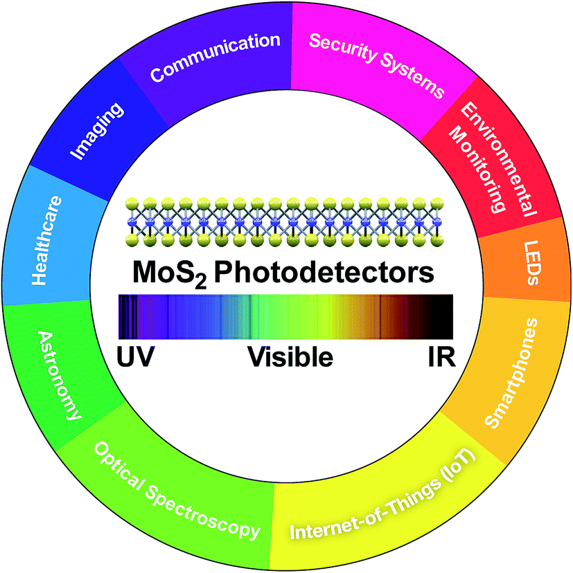 | ||
| Fig. 29 Applications of atomic layered MoS2 based ultra-broadband photodetectors. | ||
9. Conclusions and perspective
The role of 2D TMDs, especially atomic layered MoS2 and its diverse vdWHs, in developing photodetectors for optoelectronic applications has been discussed, where the photoresponse can be tailored over a broad spectral range from UV to IR regions. The review has particularly summarized the progress made in the design and fabrication of broadband photodetectors using atomic layered MoS2 and MoS2-based hybrid heterostructures for wearable optoelectronics. The performance of MoS2 photodetectors can be dramatically improved and optimized by forming MoS2 hybrid heterostructures with 0D QDs,193,194 2D materials,169,196,226,281,309,329,334–336 ferroelectric polymers,137,324 halide perovskites,179,191,192,327 piezo-phototronic effect,221,258,272 and via chemical doping,187,326 as has been studied for the phototransistor, photodiode and photoconductor components. The photoresponsivity, detectivity and photoresponse of MoS2 hybrid heterostructure-based photodetectors vary by several orders of magnitude depending on the nature of the vdWHs, doping agents, optical wavelengths and intensity of applied incident power.122,171,178,179,199,226,321,325,326,326 Temperature-dependent ultrahigh photoresponsivities of 5 × 10⁸ A W−1 to 1 × 10¹⁰ A W−1 have been observed for the monolayer graphene/ML MoS2 hybrid vdWH-based photodetectors.122 Similarly, an ultrahigh detectivity of 3.8 × 10¹⁵ Jones was recorded for the rGO–MoS2/pyramid Si hybrid heterostructure-based photodetector, which also operated in the ultra-broadband spectral range of 350 nm to 4.3 μm (UV to MIR) due to the bandgap narrowing instigated by the sulfur (S) vacancy defects in MoS2 crystals.178 The MoS2 hybrid heterostructure-based photodetectors also exhibit improved environmental stability for extended periods of time.162,187,192 The flexible photodetectors developed from MoS2 layers and MoS2 hybrids with TMDs, graphene, CNTs, and ZnO and their applications in wearable optoelectronics have been discussed. The figures-of-merit of a very wide range of MoS2-based photodetectors have been compared in terms of their important parameters including photoresponsivity, detectivity, and response speed measured at different wavelengths and incident laser power densities.The integration of MoS2 photodetectors with other flexible electronic, photonic and optoelectronic functional devices remains challenging. Research activities on MoS2 based photodetectors is emerging on a fast pace.446–451 The large family of 2D materials can be explored for developing photodetection devices. For example, 2D TMDs such as MoSe2, MoTe2, WS2, WSe2, PtS2, PtSe2, PtTe2, PdS2, PdSe2, PdTe2, GeS2, GeSe2, HfS2, TiS2, FeS2, CoS2, NiS2, SnS2, MoSe2, NbSe2, TaSe2, NiSe2, FeSe2, and CoSe2 can be explored for developing new vdWHs for high-performance photodetectors. Tremendous opportunities exist for TMD-based vdWHs with other nanomaterials, including BP, graphene, h-BN, Janus TMDs, mono-chalcogenide layered materials (GaS, GaSe, GaTe, InS, InSe, InTe, SnS, SnSe, SnTe, PbS, PbTe, etc.), 2D transition-metal carbides, nitrides and carbonitrides (MXenes), transition-metal trichalcogenides (MX3; M = Ti, Zr, Hf, Nb, Ta, and X = S, Se, Te), perovskites, surface-functionalized 2D TMDs and transition metal oxides (TMOs), inorganic semiconductors and organic materials, which represent the future direction of TMD-based photodetectors for their application in fields from biomedical imaging to optical communication. TMDs are also advancing as multifunctional materials for future wearable electronic and optoelectronic devices as an inexpensive alternative to the costly manufactured semiconducting materials currently employed in the electronics industry. 2D atomic layered material-based hybrid vdWHs hold great potential for self-powered flexible photodetectors in the healthcare industry especially for biomedical imaging, point-of-care wearable biosensors for monitoring vital signs and metabolic parameters, cardiac pacemakers, and for patients. There are many significant challenges to producing low-cost, large-scale high-performance photodetector devices for commercial applications, therefore factors such as optimization of the photoresponse, reproducibility, long-term environmental stability of photodetector devices, mechanical flexibility, packaging, and the toxicity of nanomaterials452–460 used in photodetectors need much more attention. TMDs are very promising nanomaterials for developing high-performance flexible photodetectors and for integration of such devices into the next generation of wearable technologies.
Disclaimer
The author cannot accept liability for any kind of scientific and technical data contained in this review article whatsoever for any omissions or any errors or the accuracy of contents or a claim of completeness.Conflicts of interest
There are no conflicts to declare.Acknowledgements
The author wishes to thank Eric Singh at Stanford University, Ravina Singh at the Wharton School of Business, University of Pennsylvania, Dr Surya Singh at the University of Oxford, and David Tebera for their valuable support. This work was sponsored by American Scientific Publishers, Los Angeles, California.References
- RP Photonics Encyclopedia (formerly Encyclopedia of Laser Physics and Technology), RP Photonics Consulting GmbH, Bad Dürrheim, Germany, 2013, https://www.rp-photonics.com.
- (a) Handbook of Advanced Electronic and Photonic Materials and Devices, ed. H. S. Nalwa, Academic Press, San Diego, 2001, 10-volume set Search PubMed; (b) Handbook of Organic Electronics and Photonics, ed. H. S. Nalwa, American Scientific Publishers, Los Angeles, 2008, 3-volume set Search PubMed; (c) Handbook of Luminescence, Display Materials and Devices, ed. H. S. Nalwa and L. S. Rohwer, American Scientific Publishers, Los Angeles, 2003, 3-volume set Search PubMed; (d) Encyclopedia of Nanoscience and Nanotechnology, ed. H. S. Nalwa, American Scientific Publishers, Los Angeles, 2004, 10-volume set Search PubMed.
- T. Ma, Z. Liu, J. Wen, Y. Gao, X. Ren, H. Chen, C. Jin, X.-L. Ma, N. Xu, H.-M. Cheng and W. Ren, Tailoring the Thermal and Electrical Transport Properties of Graphene Films by Grain Size Engineering, Nat. Commun., 2017, 8, 14486 CrossRef CAS PubMed.
- Z. Zhang, H. Huang, X. Yang and L. Zang, Tailoring Electronic Properties of Graphene by π–π Stacking with Aromatic Molecules, J. Phys. Chem. Lett., 2011, 2, 2897–2905 CrossRef CAS.
- D. Wang, L. Wang, X. Dong, Z. Shi and J. Jin, Chemically Tailoring Graphene Oxides into Fluorescent Nanosheets for Fe3+ ion Detection, Carbon, 2012, 50, 2147–2154 CrossRef CAS.
- D. Qu, M. Zheng, J. Li, Z. Xie and Z. Sun, Tailoring Color Emissions from N-Doped Graphene Quantum Dots for Bioimaging Applications, Light: Sci. Appl., 2015, 4, e364 CrossRef CAS.
- M. Yi and Z. Shen, A Review on Mechanical Exfoliation for the Scalable Production of Graphene, J. Mater. Chem. A, 2015, 3, 11700–11715 RSC.
- (a) E. Singh and H. S. Nalwa, Graphene-Based Bulk-Heterojunction Solar Cells: A Review, J. Nanosci. Nanotechnol., 2015, 15, 6237–6278 CrossRef CAS PubMed; (b) E. Singh and H. S. Nalwa, Stability of graphene-based heterojunction solar cells, RSC Adv., 2015, 5, 73575–73600 RSC.
- E. Singh and H. S. Nalwa, Graphene-Based Dye-Sensitized Solar Cells: A Review, Sci. Adv. Mater., 2015, 7, 1863–1912 CrossRef CAS.
- R. Muñoz and C. Gómez-Aleixandre, Review of CVD Synthesis of Graphene, Chem. Vap. Deposition, 2013, 19, 297–322 CrossRef.
- S. Bae, H. Kim, Y. Lee, X. Xu, J.-S. Park, Y. Zheng, J. Balakrishnan, T. Lei, H. Ri Kim, Y. I. Song, Y.-J. Kim, K. S. Kim, B. Özyilmaz, J.-H. Ahn, B. H. Hong and S. Iijima, Roll-to-Roll Production of 30-Inch Graphene Films for Transparent Electrodes, Nat. Nanotechnol., 2010, 5, 574–578 CrossRef CAS.
- K. S. Kim, Y. J. Ji, Y. Nam, K. H. Kim, E. Singh, J. Y. Lee and G. Y. Yeom, Atomic Layer Etching of Graphene Through Controlled Ion Beam for Graphene-Based Electronics, Sci. Rep., 2017, 7, 2462 CrossRef PubMed.
- H. Wang, H. Yuan, S. S. Hong, Y. Li and Y. Cui, Physical and Chemical Tuning of Two-Dimensional Transition Metal Dichalcogenides, Chem. Soc. Rev., 2015, 44, 2664–2680 RSC.
- C. R. Ryder, J. D. Wood, S. A. Wells and M. C. Hersam, Chemically Tailoring Semiconducting Two-Dimensional Transition Metal Dichalcogenides and Black Phosphorus, ACS Nano, 2016, 10, 3900–3917 CrossRef CAS PubMed.
- S. Najmaei, X. Zou, D. Er, J. Li, Z. Jin, W. Gao, Q. Zhang, S. Park, L. Ge, S. Lei, J. Kono, V. B. Shenoy, B. I. Yakobson, A. George, P. M. Ajayan and J. Lou, Tailoring the Physical Properties of Molybdenum Disulfide Monolayers by Control of Interfacial Chemistry, Nano Lett., 2014, 14, 1354–1361 CrossRef CAS PubMed.
- M. Chhowalla, H. S. Shin, G. Eda, L.-J. Li, K. P. Loh and H. Zhang, The Chemistry of Two-Dimensional Layered Transition Metal Dichalcogenide Nanosheets, Nat. Chem., 2013, 5, 263–275 CrossRef PubMed.
- R. Lv, J. A. Robinson, R. E. Schaak, D. Sun, Y. Sun, T. E. Mallouk and M. Terrones, Transition Metal Dichalcogenides and Beyond: Synthesis, Properties, and Applications of Single- and Few-Layer Nanosheets, Acc. Chem. Res., 2014, 48, 56–64 CrossRef PubMed.
- M. Chhowalla, Z. Liu and H. Zhang, Two-Dimensional Transition Metal Dichalcogenide (TMD) Nanosheets, Chem. Soc. Rev., 2015, 44, 2584–2586 RSC.
- Y. Shi, H. Li and L.-J. Li, Recent Advances in Controlled Synthesis of Two-Dimensional Transition Metal Dichalcogenides Via Vapour Deposition Techniques, Chem. Soc. Rev., 2015, 44, 2744–2756 RSC.
- K. S. Kim, K. H. Kim, Y. Nam, J. Jeon, S. Yim, E. Singh, J. Y. Lee, S. J. Lee, Y. S. Jung, G. Y. Yeom and D. W. Kim, Atomic Layer Etching Mechanism of MoS2 for Nanodevices, ACS Appl. Mater. Interfaces, 2017, 9, 11967–11976 CrossRef CAS PubMed.
- B. J. Kim, H. Jang, S.-K. Lee, B. H. Hong, J.-H. Ahn and J. H. Cho, High-Performance Flexible Graphene Field Effect Transistors with Ion Gel Gate Dielectrics, Nano Lett., 2010, 10, 3464–3466 CrossRef CAS.
- S. J. Park, O. S. Kwon, S. H. Lee, H. S. Song, T. H. Park and J. Jang, Ultrasensitive Flexible Graphene Based Field-Effect Transistor (FET)-Type Bioelectronic Nose, Nano Lett., 2012, 12, 5082–5090 CrossRef CAS PubMed.
- Nanomaterial-Based Flexible and Multifunctional Sensors, ed. E. Singh and H. S. Nalwa, American Scientific Publishers, Los Angeles, California, 2019 Search PubMed.
- R. Singh, E. Singh and H. S. Nalwa, Inkjet Printed Nanomaterial Based Flexible Radio Frequency Identification (RFID) Tag Sensors for the Internet of Nano Things, RSC Adv., 2017, 7, 48597–48630 RSC.
- (a) E. Singh, M. Meyyappan and H. S. Nalwa, Flexible Graphene-Based Wearable Gas and Chemical Sensors, ACS Appl. Mater. Interfaces, 2017, 9, 34544–34586 CrossRef CAS PubMed; (b) E. Singh, M. Meyyappan and H. S. Nalwa, Graphene-Based Flexible and Stretchable Strain Sensors for Wearable Electronics, Chapter 1, in Nanomaterial-Based Flexible and Multifunctional Sensors, ed. E. Singh and H. S. Nalwa, American Scientific Publishers, Los Angeles, California, 2019, pp.1–50 Search PubMed.
- S. K. Krishnan, E. Singh, P. Singh, M. Meyyappan and H. S. Nalwa, A Review on Graphene-Based Nanocomposites for Electrochemical and Fluorescent Biosensors, RSC Adv., 2019, 9, 8778–8881 RSC.
- W. K. Chee, H. N. Lim, Z. Zainal, N. M. Huang, I. Harrison and Y. Andou, Flexible Graphene-Based Supercapacitors: A Review, J. Phys. Chem. C, 2016, 120, 4153–4172 CrossRef CAS.
- S. H. Aboutalebi, R. Jalili, D. Esrafilzadeh, M. Salari, Z. Gholamvand, S. A. Yamini, K. Konstantinov, R. L. Shepherd, J. Chen, S. E. Moulton, P. C. Innis, A. I. Minett, J. M. Razal and G. G. Wallace, High-Performance Multifunctional Graphene Yarns: Toward Wearable All-Carbon Energy Storage Textiles, ACS Nano, 2014, 8, 2456–2466 CrossRef CAS PubMed.
- N. Li, Z. Chen, W. Ren, F. Li and H. M. Cheng, Flexible Graphene-Based Lithium Ion Batteries with Ultrafast Charge and Discharge Rates, Proc. Natl. Acad. Sci. U. S. A., 2012, 109, 17360–17365 CrossRef CAS PubMed.
- S. Kim, M. K. Gupta, K. Y. Lee, A. Sohn, T. Y. Kim, K.-S. Shin, D. Kim, S. K. Kim, K. H. Lee, H.-J. Shin, D.-W. Kim and S.-W. Kim, Transparent Flexible Graphene Triboelectric Nanogenerators, Adv. Mater., 2014, 26, 3918–3925 CrossRef CAS PubMed.
- K. Ruan, K. Ding, Y. Wang, S. Diao, Z. Shao, X. Zhang and J. Jie, Flexible Graphene/Silicon Heterojunction Solar Cells, J. Mater. Chem. A, 2015, 3, 14370–14377 RSC.
- I. A. Sahito, K. C. Sun, A. A. Arbab, M. B. Qadir, Y. S. Choi and S. H. Jeong, Flexible and Conductive Cotton Fabric Counter Electrode Coated with Graphene Nanosheets for High Efficiency Dye Sensitized Solar Cell, J. Power Sources, 2016, 319, 90–98 CrossRef CAS.
- T. Jiao, D. Wei, J. Liu, W. Sun, S. Jia, W. Zhang, Y. Feng, H. Shi and C. Du, Flexible Solar Cells Based on Graphene-Ultrathin Silicon Schottky Junction, RSC Adv., 2015, 5, 73202–73206 RSC.
- N. Liu, H. Tian, G. Schwartz, J. B. H. Tok, T.-L. Ren and Z. Bao, Large-Area, Transparent, and Flexible Infrared Photodetector Fabricated Using P-N Junctions Formed by N-Doping Chemical Vapor Deposition Grown Graphene, Nano Lett., 2014, 14, 3702–3708 CrossRef CAS PubMed.
- H. Tetsuka, A. Nagoya and S.-I. Tamura, Graphene/Nitrogen-Functionalized Graphene Quantum Dot Hybrid Broadband Photodetectors with a Buffer Layer of Boron Nitride Nanosheets, Nanoscale, 2016, 8, 19677–19683 RSC.
- E. Singh, P. Singh, K. S. Kim, G. Y. Yeom and H. S. Nalwa, Flexible Molybdenum Disulfide (MoS2) Atomic Layers for Wearable Electronics and Optoelectronics, ACS Appl. Mater. Interfaces, 2019, 11, 11061–11105 CrossRef CAS PubMed.
- H.-Y. Chang, S. Yang, J. Lee, L. Tao, W.-S. Hwang, D. Jena, N. Lu and D. Akinwande, High-Performance, Highly Bendable MoS2 Transistors with High-κ Dielectrics for Flexible Low-Power Systems, ACS Nano, 2013, 7, 5446–5452 CrossRef CAS PubMed.
- C. Kuru, D. Choi, A. Kargar, C. H. Liu, S. Yavuz, C. Choi, S. Jin and P. R. Bandaru, High-Performance Flexible Hydrogen Sensor Made of WS2 Nanosheet–Pd Nanoparticle Composite Film, Nanotechnology, 2016, 27, 195501 CrossRef PubMed.
- J. Y. Oh, J. H. Lee, S. W. Han, S. S. Chae, E. J. Bae, Y. H. Kang, W. J. Choi, S. Y. Cho, J.-O. Lee, H. K. Baik and T. I. Lee, Chemically Exfoliated Transition Metal Dichalcogenide Nanosheet-Based Wearable Thermoelectric Generators, Energy Environ. Sci., 2016, 9, 1696–1705 RSC.
- Y. Xiao, L. Huang, Q. Zhang, S. Xu, Q. Chen and W. Shi, Gravure Printing of Hybrid MoS2@S-rGO Interdigitated Electrodes for Flexible Microsupercapacitors, Appl. Phys. Lett., 2015, 107, 013906 CrossRef.
- (a) Photodetectors and Fiber Optics, ed. H. S. Nalwa, Academic Press, San Diego, 2001 Search PubMed; (b) Polymer Optical Fibers, ed. H. S. Nalwa, American Scientific Publishers, Los Angeles, 2004 Search PubMed; (c) Silicon-Based Materials and Devices, ed. H. S. Nalwa, Academic Press, San Diego, 2001, 2-volume set Search PubMed; (d) Handbook of Thin Films, ed. H. S. Nalwa, Academic Press, San Diego, 2001, 5-volume set Search PubMed; (e) Handbook of Surfaces and Interfaces of Materials, ed. H. S. Nalwa, Academic Press, San Diego, 2001, 5-volume set Search PubMed; (f) Handbook of Organic Conductive Molecules and Polymers, ed. H. S. Nalwa, Wiley, Chichester, 1997, 4-volume set Search PubMed; (g) Supramolecular Photosensitive and Electroactive Materials, ed. H. S. Nalwa, Academic Press, San Diego, 2001 Search PubMed; (h) Handbook of Nanostructured Materials and Nanotechnology, ed. H. S. Nalwa, Academic Press, San Diego, 1999, 5-volume set Search PubMed.
- M. Dang, H.-C. Yuan, Z. Ma, J. Ma and G. Qin, The Fabrication and Characterization of Flexible Single-Crystalline Silicon and Germanium p-Intrinsic-n Photodetectors on Plastic Substrates, Appl. Phys. Lett., 2017, 110, 253104 CrossRef.
- H.-C. Yuan, J. Shin, G. Qin, L. Sun, P. Bhattacharya, M. G. Lagally, G. K. Celler and Z. Ma, Flexible Photodetectors on Plastic Substrates by Use of Printing Transferred Single-Crystal Germanium Membranes, Appl. Phys. Lett., 2009, 94, 013102 CrossRef.
- L.-B. Luo, X.-B. Yang, F.-X. Liang, J.-S. Jie, Q. Li, Z.-F. Zhu, C.-Y. Wu, Y.-Q. Yu and L. Wang, Transparent and Flexible Selenium Nanobelt-Based Visible Light Photodetector, CrystEngComm, 2012, 14, 1942–1947 RSC.
- G. Chen, X. Xie and G. Shen, Flexible Organic-Inorganic Hybrid Photodetectors with n-Type Phenyl-C61-Butyric Acid Methyl Ester (PCBM) and p-Type Pearl-Like GaP Nanowires, Nano Res., 2014, 7, 1777–1787 CrossRef CAS.
- G. Chen, B. Liang, Z. Liu, G. Yu, X. Xie, T. Luo, Z. Xie, D. Chen, M.-Q. Zhu and G. Shen, High Performance Rigid and Flexible Visible-Light Photodetectors Based on Aligned X(In, Ga)P Nanowire Arrays, J. Mater. Chem. C, 2014, 2, 1270–1277 RSC.
- K. Heo, H. Lee, Y. Park, J. Park, H.-J. Lim, D. Yoon, C. Lee, M. Kim, H. Cheong, J. Park, J. Jian and S. Hong, Aligned Networks of Cadmium Sulfide nanowires for Highly Flexible Photodetectors with Improved Photoconductive Responses, J. Mater. Chem., 2012, 22, 2173–2179 RSC.
- L. Li, Z. Lou and G. Shen, Hierarchical CdS Nanowires Based Rigid and Flexible Photodetectors with Ultrahigh Sensitivity, ACS Appl. Mater. Interfaces, 2015, 7, 23507–23514 CrossRef CAS PubMed.
- Z. Wang, J. Jie, F. Li, L. Wang, T. Yan, L. Luo, B. Nie, C. Xie, P. Jiang, X. Zhang, Y. Yu and C. Wu, Chlorine-Doped ZnSe Nanoribbons with Tunable n-Type Conductivity as High-Gain and Flexible Blue/UV Photodetectors, ChemPlusChem, 2012, 77, 470–475 CrossRef CAS.
- J. M. Wu, Y.-R. Chen and Y.-H. Lin, Rapidly Synthesized ZnO Nanowires by Ultraviolet Decomposition Process in Ambient Air for Flexible Photodetector, Nanoscale, 2011, 3, 1053–1058 RSC.
- Z. Zheng, L. Gan, J. Zhang, F. Zhuge and T. Zhai, An Enhanced UV-Vis-NIR and Flexible Photodetector Based on Electrospun ZnO Nanowire Array/PbS Quantum Dots Film Heterostructure, Adv. Sci., 2017, 4, 1600316 CrossRef PubMed.
- W. Tian, C. Zhang, T. Zhai, S.-L. Li, X. Wang, J. Liu, X. Jie, D. Liu, M. Liao, Y. Koide, D. Golberg and Y. Bando, Flexible Ultraviolet Photodetectors with Broad Photoresponse Based on Branched ZnS-ZnO Heterostructure Nanofilms, Adv. Mater., 2014, 26, 3088–3093 CrossRef CAS PubMed.
- Z. Zheng, L. Gan, H. Li, Y. Ma, Y. Bando, D. Golberg and T. Zhai, A Fully Transparent and Flexible Ultraviolet-Visible Photodetector Based on Controlled Electrospun ZnO-CdO Heterojunction Nanofiber Arrays, Adv. Funct. Mater., 2015, 25, 5885–5894 CrossRef CAS.
- Z. Jin, L. Gao, Q. Zhou and J. Wang, High-Performance Flexible Ultraviolet Photoconductors Based on Solution-Processed Ultrathin ZnO/Au Nanoparticle Composite Films, Sci. Rep., 2014, 4, 4268 CrossRef PubMed.
- F.-X. Wang, J.-M. Yang, S.-H. Nie, W.-M. Su and G.-B. Pan, All Solution-Processed Large-Area Patterned Flexible Photodetectors Based on ZnOEP/PVK Hybrid Film, J. Mater. Chem. C, 2016, 4, 7841–7845 RSC.
- Z. Lou, L. Li and G. Shen, High-Performance Rigid and Flexible Ultraviolet Photodetectors with Single-Crystalline ZnGa2O4 Nanowires, Nano Res., 2015, 8, 2162–2169 CrossRef CAS.
- Z. Liu, H. Huang, B. Liang, X. Wang, Z. Wang, D. Chen and G. Shen, Zn2GeO4 and In2Ge2O7 Nanowire Mats Based Ultraviolet Photodetectors on Rigid and Flexible Substrates, Opt. Express, 2012, 20, 2982–2991 CrossRef CAS.
- W. Bi, M. Zhou, Z. Ma, H. Zhang, J. Yu and Y. Xie, CuInSe2 Ultrathin Nanoplatelets: Novel Self-Sacrificial Template-Directed Synthesis and Application for Flexible Photodetectors, Chem. Commun., 2012, 48, 9162–9164 RSC.
- Y. Min, G. D. Moon, J. Park, M. Park and U. Jeong, Surfactant-Free CuInSe2 Nanocrystals Transformed from In2Se3 Nanoparticles and Their Application for a Flexible UV Photodetector, Nanotechnology, 2011, 22, 465604 CrossRef PubMed.
- X. Xie and G. Shen, Single-Crystalline In2S3 Nanowire-Based Flexible Visible-Light Photodetectors with an Ultra-High Photoresponse, Nanoscale, 2015, 7, 5046–5052 RSC.
- Z. Q. Zheng, J. D. Yao and G. W. Yang, Growth of Centimeter-Scale High-Quality In2Se3 Films for Transparent, Flexible and High Performance Photodetectors, J. Mater. Chem. C, 2016, 4, 8094–8103 RSC.
- J. Chao, B. Liang, X. Hou, Z. Liu, Z. Xie, B. Liu, W. Song, G. Chen, D. Chen and G. Shen, Selective Synthesis of Sb2S3 Nanoneedles and Nanoflowers for High Performance Rigid and Flexible Photodetectors, Opt. Express, 2013, 21, 13639–13647 CrossRef CAS PubMed.
- Y. Liang, Y. Wang, J. Wang, S. Wu, D. Jiang and J. Lian, High-Performance Flexible Photodetectors Based on Single-Crystalline Sb2Se3 Nanowires, RSC Adv., 2016, 6, 11501–11506 RSC.
- G. Chen, Y. Yu, K. Zheng, T. Ding, W. Wang, Y. Jiang and Q. Yang, Fabrication of Ultrathin Bi2S3 Nanosheets for High-Performance, Flexible, Visible-NIR Photodetectors, Small, 2015, 11, 2848–2855 CrossRef CAS PubMed.
- G. M. Kumar, X. Fu, P. Ilanchezhiyan, S. U. Yuldashev, D. J. Lee, H. D. Cho and T. W. Kang, Highly Sensitive Flexible Photodetectors Based on Self-Assembled Tin Monosulfide Nanoflakes with Graphene Electrodes, ACS Appl. Mater. Interfaces, 2017, 9, 32142–32150 CrossRef PubMed.
- Y. Tao, X. Wu, W. Wang and J. Wang, Flexible Photodetector from Ultraviolet to Near Infrared Based on a SnS2 Nanosheet Microsphere Film, J. Mater. Chem. C, 2015, 3, 1347–1353 RSC.
- Y.-R. Tao, X.-C. Wu and W.-W. Xiong, Flexible Visible-Light Photodetectors with Broad Photoresponse Based on ZrS3 Nanobelt Films, Small, 2014, 10, 4905–4911 CrossRef CAS PubMed.
- G. Yu, B. Liang, H. Huang, G. Chen, Z. Liu, D. Chen and G. Shen, Contact Printing of Horizontally-Aligned p-type Zn3P2 Nanowire Arrays for Rigid and Flexible Photodetectors, Nanotechnology, 2013, 24, 095703 CrossRef PubMed.
- M. Zhong, L. Huang, H.-X. Deng, X. Wang, B. Li, Z. Wei and J. Li, Flexible Photodetectors Based on Phase Dependent PbI2 Single Crystals, J. Mater. Chem. C, 2016, 4, 6492–6499 RSC.
- Q. Zheng, J. Huang, S. Cao and H. Gao, A Flexible Ultraviolet Photodetector Based on Single Crystalline MoO3 Nanosheets, J. Mater. Chem. C, 2015, 3, 7469–7475 RSC.
- P. Hu, L. Wang, M. Yoon, J. Zhang, W. Feng, X. Wang, Z. Wen, J. C. Idrobo, Y. Miyamoto, D. B. Geohegan and K. Xiao, Highly Responsive Ultrathin GaS Nanosheet Photodetectors on Rigid And Flexible Substrates, Nano Lett., 2013, 13, 1649–1654 CrossRef CAS PubMed.
- X. Hou, B. Liu, X. Wang, Z. Wang, Q. Wang, D. Chen and G. Shen, SnO2-Microtube-Assembled Cloth for Fully Flexible Self-Powered Photodetector Nanosystems, Nanoscale, 2013, 5, 7831–7837 RSC.
- Z. Liu, G. Chen, B. Liang, G. Yu, H. Huang, D. Chen and G. Shen, Fabrication of High-Quality ZnTe Nanowires Toward High-Performance Rigid/Flexible Visible-Light Photodetectors, Opt. Express, 2013, 21, 7799–7810 CrossRef CAS PubMed.
- F. Liu, H. Shimotani, H. Shang, T. Kanagasekaran, V. Zólyomi, N. Drummond, V. I. Fal’ko and K. Tanigaki, High-Sensitivity Photodetectors Based on Multilayer GaTe Flakes, ACS Nano, 2014, 8, 752–760 CrossRef CAS PubMed.
- G. Tong, H. Li, D. Li, Z. Zhu, E. Xu, G. Li, L. Yu, J. Xu and Y. Jiang, Dual-Phase CsPbBr3-CsPb2Br5 Perovskite Thin Films via Vapor Deposition for High-Performance Rigid and Flexible Photodetectors, Small, 2018, 14, 1702523 CrossRef PubMed.
- B. Sun, S. Xi, Z. Liu, X. Liu, Z. Wang, X. Tan, T. Shi, J. Zhou and G. Liao, Sensitive, fast, and stable photodetector based on perovskite/MoS2 hybrid film, Appl. Surf. Sci., 2019, 493, 389–395 CrossRef CAS.
- T. Gao, Q. Zhang, J. Chen, X. Xiong and T. Zhai, Performance-Enhancing Broadband and Flexible Photodetectors Based on Perovskite/ZnO-Nanowire Hybrid Structures, Adv. Opt. Mater., 2017, 5, 1700206 CrossRef.
- C. Bao, W. Zhu, J. Yang, F. Li, S. Gu, Y. Wang, T. Yu, J. Zhu, Y. Zhou and Z. Zou, Highly Flexible Self-Powered Organolead Trihalide Perovskite Photodetectors with Gold Nanowire Networks as Transparent Electrodes, ACS Appl. Mater. Interfaces, 2016, 8, 23868–23875 CrossRef CAS PubMed.
- S. Chen, C. Teng, M. Zhang, Y. Li, D. Xie and G. Shi, A Flexible UV-Vis-NIR Photodetector Based on a Perovskite/Conjugated-Polymer Composite, Adv. Mater., 2016, 28, 5969–5974 CrossRef CAS PubMed.
- V. Q. Dang, G.-S. Han, T. Q. Trung, L. T. Duy, Y.-U. Jin, B.-U. Hwang, H.-S. Jung and N.-E. Lee, Methylammonium Lead Iodide Perovskite-Graphene Hybrid Channels in Flexible Broadband Phototransistors, Carbon, 2016, 105, 353–361 CrossRef CAS.
- L. Tong, C. Li, F. E. Chen, H. Bai, L. Zhao and G. Shi, Flexible Sandwich Photodetectors Based on Thick Polythiophene Films, J. Phys. Chem. C, 2009, 113, 7411–7415 CrossRef CAS.
- A. Falco, L. Cinà, G. Scarpa, P. Lugli and A. Abdellah, Fully-Sprayed and Flexible Organic Photodiodes with Transparent Carbon Nanotube Electrodes, ACS Appl. Mater. Interfaces, 2014, 6, 10593–10601 CrossRef CAS PubMed.
- Y. Liu, Y. Liu, S. Qin, Y. Xu, R. Zhang and F. Wang, Graphene-Carbon Nanotube Hybrid Films for High-Performance Flexible Photodetectors, Nano Res., 2017, 10, 1880–1887 CrossRef CAS.
- D. I. Son, H. Y. Yang, T. W. Kim and W. I. Park, Transparent and Flexible Ultraviolet Photodetectors Based on Colloidal ZnO Quantum Dot/Graphene Nanocomposites Formed on Poly(Ethylene Terephthalate) Substrates, Composites, Part B, 2015, 69, 154–158 CrossRef CAS.
- Y.-R. Tao, J.-Q. Chen, J.-J. Wu, Y. Wu and X.-C. Wu, Flexible Ultraviolet–Visible Photodetector Based on HfS3 Nanobelt Film, J. Alloys Compd., 2016, 658, 6–11 CrossRef CAS.
- L. Fan, Y. Tao, X. Wu, Z. Wu and J. Wu, HfX3 (X = Se and S)/Graphene Composites for Flexible Photodetectors from Visible to Near-Infrared, Mater. Res. Bull., 2017, 93, 21–27 CrossRef CAS.
- Y.-L. Liu, C.-C. Yu, K.-T. Lin, T.-C. Yang, E.-Y. Wang, H.-L. Chen, L.-C. Chen and K.-H. Chen, Transparent, Broadband, Flexible, and Bifacial-Operable Photodetectors Containing a Large-Area Graphene–Gold Oxide Heterojunction, ACS Nano, 2015, 9, 5093–5103 CrossRef CAS PubMed.
- Z. Gao, W. Jin, Y. Zhou, Y. Dai, B. Yu, C. Liu, W. Xu, Y. Li, H. Peng, Z. Liu and L. Dai, Self-Powered Flexible and Transparent Photovoltaic Detectors Based on CdSe Nanobelt/Graphene Schottky Junctions, Nanoscale, 2013, 5, 5576–5581 RSC.
- F. H. L. Koppens, T. Mueller, P. Avouris, A. C. Ferrari, M. S. Vitiello and M. Polini, Photodetectors Based on Graphene, Other Two-Dimensional Materials and Hybrid Systems, Nat. Nanotechnol., 2014, 9, 780–793 CrossRef CAS PubMed.
- F. Xia, H. Wang, D. Xiao, M. Dubey and A. Ramasubramaniam, Two-Dimensional Material Nanophotonics, Nat. Photonics, 2014, 8, 899–907 CrossRef CAS.
- K. Watanabe, T. Taniguchi and H. Kanda, Direct-Bandgap Properties and Evidence for Ultraviolet Lasing of Hexagonal Boron Nitride Single Crystal, Nat. Mater., 2004, 3, 404–409 CrossRef CAS PubMed.
- N. Alem, R. Erni, C. Kisielowski, M. D. Rossell, W. Gannett and A. Zettl, Atomically Thin Hexagonal Boron Nitride Probed by Ultrahigh-Resolution Transmission Electron Microscopy, Phys. Rev. B: Condens. Matter Mater. Phys., 2009, 80, 155425 CrossRef.
- L. Song, L. Ci, H. Lu, P. B. Sorokin, C. Jin, J. Ni, A. G. Kvashnin, D. G. Kvashnin, J. Lou, B. I. Yakobson and P. M. Ajayan, Large Scale Growth and Characterization of Atomic Hexagonal Boron Nitride Layers, Nano Lett., 2010, 10, 3209–3215 CrossRef CAS PubMed.
- C. R. Dean, A. F. Young, I. Meric, C. Lee, L. Wang, S. Sorgenfrei, K. Watanabe, T. Taniguchi, P. Kim, K. L. Shepard and J. Hone, Boron Nitride Substrates for High-Quality Graphene Electronics, Nat. Nanotechnol., 2010, 5, 722–726 CrossRef CAS PubMed.
- Q. Weng, X. Wang, X. Wang, Y. Bando and D. Golberg, Functionalized Hexagonal Boron Nitride Nanomaterials: Emerging Properties and Applications, Chem. Soc. Rev., 2016, 45, 3989–4012 RSC.
- K. F. Mak, C. Lee, J. Hone, J. Shan and T. F. Heinz, Atomically thin MoS2: A New Direct-Gap Semiconductor, Phys. Rev. Lett., 2010, 105, 136805 CrossRef PubMed.
- A. Splendiani, L. Sun, Y. Zhang, T. Li, J. Kim, C.-Y. Chim, G. Galli and F. Wang, Emerging Photoluminescence in Monolayer MoS2, Nano Lett., 2010, 10, 1271–1275 CrossRef CAS PubMed.
- Y. P. V. Subbaiah, K. J. Saji and A. Tiwari, Atomically Thin MoS2: A Versatile Nongraphene 2D Material, Adv. Funct. Mater., 2016, 26, 2046–2069 CrossRef.
- H. Liu, A. T. Neal, Z. Zhu, Z. Luo, X. Xu, D. Tománek and P. D. Ye, Phosphorene: An Unexplored 2D Semiconductor with a High Hole Mobility, ACS Nano, 2014, 8, 4033–4041 CrossRef CAS PubMed.
- L. Kou, C. Chen and S. C. Smith, Phosphorene: Fabrication, Properties, and Applications, J. Phys. Chem. Lett., 2015, 6, 2794–2805 CrossRef CAS PubMed.
- H. Liu, Y. Du, Y. Deng and P. D. Ye, Semiconducting Black Phosphorus: Synthesis, Transport Properties and Electronic Applications, Chem. Soc. Rev., 2015, 44, 2732–2743 RSC.
- K. S. Novoselov, A. K. Geim, S. V. Morozov, D. Jiang, M. I. Katsnelson, I. V. Grigorieva, S. V. Dubonos and A. A. Firsov, Two-Dimensional Gas of Massless Dirac Fermions in Graphene, Nature, 2005, 438, 197–200 CrossRef CAS PubMed.
- A. K. Geim, Graphene: Status and Prospects, Science, 2009, 324, 1530–1534 CrossRef CAS PubMed.
- R. R. Nair, P. Blake, A. N. Grigorenko, K. S. Novoselov, T. J. Booth, T. Stauber, N. M. R. Peres and A. K. Geim, Fine Structure Constant Defines Visual Transparency of Graphene, Science, 2008, 320, 1308 CrossRef CAS PubMed.
- K. K. Kim, A. Hsu, X. Jia, S. M. Kim, Y. Shi, M. Dresselhaus, T. Palacios and J. Kong, Synthesis and Characterization of Hexagonal Boron Nitride Film as a Dielectric Layer for Graphene Devices, ACS Nano, 2012, 6, 8583–8590 CrossRef CAS PubMed.
- Y. Cai, G. Zhang and Y.-W. Zhang, Electronic Properties of Phosphorene/Graphene and Phosphorene/Hexagonal Boron Nitride Heterostructures, J. Phys. Chem. C, 2015, 119, 13929–13936 CrossRef CAS.
- G.-H. Lee, X. Cui, Y. D. Kim, G. Arefe, X. Zhang, C.-H. Lee, F. Ye, K. Watanabe, T. Taniguchi, P. Kim and J. Hone, Highly Stable, Dual-Gated MoS2 Transistors Encapsulated by Hexagonal Boron Nitride With Gate-Controllable Contact, Resistance, and Threshold Voltage, ACS Nano, 2015, 9, 7019–7026 CrossRef CAS PubMed.
- M. Okada, T. Sawazaki, K. Watanabe, T. Taniguch, H. Hibino, H. Shinohara and R. Kitaura, Direct Chemical Vapor Deposition Growth of WS2 Atomic Layers on Hexagonal Boron Nitride, ACS Nano, 2014, 8, 8273–8277 CrossRef CAS PubMed.
- M. W. Iqbal, M. Z. Iqbal, M. F. Khan, M. A. Shehzad, Y. Seo, J. H. Park, C. Hwang and J. Eom, High-Mobility and Air-Stable Single-Layer WS2 Field-Effect Transistors Sandwiched Between Chemical Vapor Deposition-Grown Hexagonal BN Films, Sci. Rep., 2015, 5, 10699 CrossRef CAS PubMed.
- F. Xia, T. Mueller, Y.-M. Lin, A. Valdes-Garcia and P. Avouris, Ultrafast Graphene Photodetector, Nat. Nanotechnol., 2009, 4, 839–843 CrossRef CAS PubMed.
- T. Mueller, F. Xia and P. Avouris, Graphene Photodetectors for High-Speed Optical Communications, Nat. Photonics, 2010, 4, 297–301 CrossRef CAS.
- X. Gan, R.-J. Shiue, Y. Gao, I. Meric, T. F. Heinz, K. Shepard, J. Hone, S. Assefa and D. Englund, Chip-Integrated Ultrafast Graphene Photodetector with High Responsivity, Nat. Photonics, 2013, 7, 883–887 CrossRef CAS.
- C.-H. Liu, Y.-C. Chang, T. B. Norris and Z. Zhong, Graphene Photodetectors with Ultra-Broadband and High Responsivity at Room Temperature, Nat. Nanotechnol., 2014, 9, 273–278 CrossRef CAS PubMed.
- F. Bonaccorso, Z. Sun, T. Hasan and A. C. Ferrari, Graphene Photonics and Optoelectronics, Nat. Photonics, 2010, 4, 611–622 CrossRef CAS.
- Q. Guo, A. Pospischil, M. Bhuiyan, H. Jiang, H. Tian, D. Farmer, B. Deng, C. Li, S.-J. Han, H. Wang, Q. Xia, T.-P. Ma, T. Mueller and F. Xia, Black Phosphorus Mid-Infrared Photodetectors with High Gain, Nano Lett., 2016, 16, 4648–4655 CrossRef CAS PubMed.
- (a) M. Bernardi, M. Palummo and J. C. Grossman, Extraordinary Sunlight Absorption and One Nanometer Thick Photovoltaics Using Two-Dimensional Monolayer Materials, Nano Lett., 2013, 13, 3664–3670 CrossRef CAS PubMed; (b) J. Wang, H. Fang, X. Wang, X. Chen, W. Lu and W. Hu, Recent progress on localized field enhanced two-dimensional material photodetectors from ultraviolet—visible to infrared, Small, 2017, 13, 1700894 CrossRef PubMed.
- W. J. Yu, Y. Liu, H. Zhou, A. Yin, Z. Li, Y. Huang and X. Duan, Highly Efficient Gate-Tunable Photocurrent Generation in Vertical Heterostructures of Layered Materials, Nat. Nanotechnol., 2013, 8, 952–958 CrossRef CAS PubMed.
- M. Massicotte, P. Schmidt, F. Vialla, K. G. Schädler, A. Reserbat-Plantey, K. Watanabe, T. Taniguchi, K. J. Tielrooij and F. H. L. Koppens, Picosecond Photoresponse in van der Waals Heterostructures, Nat. Nanotechnol., 2016, 11, 42–46 CrossRef CAS PubMed.
- Y. Gong, S. Lei, G. Ye, B. Li, Y. He, K. Keyshar, X. Zhang, Q. Wang, J. Lou, Z. Liu, R. Vajtai, W. Zhou and P. M. Ajayan, Two-Step Growth of Two-Dimensional WSe2/MoSe2 Heterostructures, Nano Lett., 2015, 15, 6135–6141 CrossRef CAS PubMed.
- D. A. Nguyen, H. M. Oh, N. T. Duong, S. Bang, S. J. Yoon and M. S. Jeong, Highly Enhanced Photoresponsivity of a Monolayer WSe2 Photodetector with Nitrogen-Doped Graphene Quantum Dots, ACS Appl. Mater. Interfaces, 2018, 10, 10322–10329 CrossRef CAS PubMed.
- X. Hong, J. Kim, S.-F. Shi, Y. Zhang, C. Jin, Y. Sun, S. Tongay, J. Wu, Y. Zhang and F. Wang, Ultrafast Charge Transfer in Atomically Thin MoS2/WS2 Heterostructures, Nat. Nanotechnol., 2014, 9, 682–686 CrossRef CAS PubMed.
- K. Roy, M. Padmanabhan, S. Goswami, T. P. Sai, G. Ramalingam, S. Raghavan and A. Ghosh, Graphene–MoS2 Hybrid Structures for Multifunctional Photoresponsive Memory Devices, Nat. Nanotechnol., 2013, 8, 826–830 CrossRef CAS PubMed.
- R. Cheng, D. Li, H. Zhou, C. Wang, A. Yin, S. Jiang, Y. Liu, Y. Chen, Y. Huang and X. Duan, Electroluminescence and Photocurrent Generation from Atomically Sharp WSe2/MoS2 Heterojunction p–n Diodes, Nano Lett., 2014, 14, 5590–5597 CrossRef CAS PubMed.
- Y. Zhu, Z. Li, L. Zhang, B. Wang, Z. Luo, J. Long, J. Yang, L. Fu and Y. Lu, High-Efficiency Monolayer Molybdenum Ditelluride Light-Emitting Diode and Photodetector, ACS Appl. Mater. Interfaces, 2018, 10, 43291–43298 CrossRef CAS PubMed.
- O. Salehzadeh, N. H. Tran, X. Liu, I. Shih and Z. Mi, Exciton Kinetics, Quantum Efficiency, and Efficiency Droop of Monolayer MoS2 Light-Emitting Devices, Nano Lett., 2014, 14, 4125–4130 CrossRef CAS PubMed.
- J. S. Ross, P. Klement, A. M. Jones, N. J. Ghimire, J. Yan, D. G. Mandrus, T. Taniguchi, K. Watanabe, K. Kitamura, W. Yao, D. H. Cobden and X. Xu, Electrically Tunable Excitonic Light-Emitting Diodes Based on Monolayer WSe2 p–n Junctions, Nat. Nanotechnol., 2014, 9, 268–272 CrossRef CAS PubMed.
- T. A. Shastry, I. Balla, H. Bergeron, S. H. Amsterdam, T. J. Marks and M. C. Hersam, Mutual Photoluminescence Quenching and Photovoltaic Effect in Large-Area Single-Layer MoS2–Polymer Heterojunctions, ACS Nano, 2016, 10, 10573–10579 CrossRef CAS PubMed.
- X. Yu and K. Sivula, Photogenerated Charge Harvesting and Recombination in Photocathodes of Solvent-Exfoliated WSe2, Chem. Mater., 2017, 29, 6863–6875 CrossRef CAS.
- G. Kakavelakis, A. E. Del Rio Castillo, V. Pellegrini, A. Ansaldo, P. Tzourmpakis, R. Brescia, M. Prato, E. Stratakis, E. Kymakis and F. Bonaccorso, Size-Tuning of WSe2 Flakes for High Efficiency Inverted Organic Solar Cells, ACS Nano, 2017, 11, 3517–3531 CrossRef CAS PubMed.
- E. Singh, K. S. Kim, G. Y. Yeom and H. S. Nalwa, Atomically Thin-Layered Molybdenum Disulfide (MoS2) for Bulk-Heterojunction Solar Cells, ACS Appl. Mater. Interfaces, 2017, 9, 3223–3245 CrossRef CAS PubMed.
- E. Singh, K. S. Kim, G. Y. Yeom and H. S. Nalwa, Two-Dimensional Transition Metal Dichalcogenide-Based Counter Electrodes for Dye-Sensitized Solar Cells, RSC Adv., 2017, 7, 28234–28290 RSC.
- G. Cao, A. Shang, C. Zhang, Y. Gong, S. Li, Q. Bao and X. Li, Optoelectronic Investigation of Monolayer MoS2/WSe2 Vertical Heterojunction Photoconversion Devices, Nano Energy, 2016, 30, 260–266 CrossRef CAS.
- L. F. Mattheiss, Band Structures of Transition-Metal-Dichalcogenide Layer Compounds, Phys. Rev. B: Solid State, 1973, 8, 3719–3740 CrossRef CAS.
- A. D. Yoffe, Layer Compounds, Annu. Rev. Mater. Sci., 1973, 3, 147–170 CrossRef CAS.
- Q. H. Wang, K. Kalantar-Zadeh, A. Kis, J. N. Coleman and M. S. Strano, Electronics and Optoelectronics of Two-Dimensional Transition Metal Dichalcogenides, Nat. Nanotechnol., 2012, 7, 699–712 CrossRef CAS PubMed.
- D. Kufer and G. Konstantatos, Highly Sensitive, Encapsulated MoS2 Photodetector with Gate Controllable Gain and Speed, Nano Lett., 2015, 15, 7307–7313 CrossRef CAS PubMed.
- X. Wang, P. Wang, J. Wang, W. Hu, X. Zhou, N. Guo, H. Huang, S. Sun, H. Shen, T. Lin, M. Tang, L. Liao, A. Jiang, J. Sun, X. Meng, X. Chen, W. Lu and J. Chu, Ultrasensitive and Broadband MoS2 Photodetector Driven by Ferroelectrics, Adv. Mater., 2015, 27, 6575–6581 CrossRef CAS PubMed.
- Y. Li, J. G. DiStefano, A. A. Murthy, J. D. Cain, E. D. Hanson, Q. Li, F. C. Castro, X. Chen and V. P. Dravid, Superior Plasmonic Photodetectors Based on Au@MoS2 Core–Shell Heterostructures, ACS Nano, 2017, 11, 10321–10329 CrossRef CAS PubMed.
- Z. P. Ling, R. Yang, J. W. Chai, S. J. Wang, W. S. Leong, Y. Tong, D. Lei, Q. Zhou, X. Gong, D. Z. Chi and K. W. Ang, Large-Scale Two-Dimensional MoS2 Photodetectors by Magnetron Sputtering, Opt. Express, 2015, 23, 13580–13586 CrossRef CAS PubMed.
- Y. Huang, W. Zheng, Y. Qiu and P. Hu, Effects of Organic Molecules with Different Structures and Absorption Bandwidth on Modulating Photoresponse of MoS2 Photodetector, ACS Appl. Mater. Interfaces, 2016, 8, 23362–23370 CrossRef CAS PubMed.
- J. Xia, X. Huang, L.-Z. Liu, M. Wang, L. Wang, B. Huang, D.-D. Zhu, J.-J. Li, C.-Z. Gu and X.-M. Meng, CVD Synthesis of Large-Area, Highly Crystalline MoSe2 Atomic Layers on Diverse Substrates and Application to Photodetectors, Nanoscale, 2014, 6, 8949–8955 RSC.
- Y.-H. Chang, W. Zhang, Y. Zhu, Y. Han, J. Pu, J.-K. Chang, W.-T. Hsu, J.-K. Huang, C.-L. Hsu, M.-H. Chiu, T. Takenobu, H. Li, C.-I. Wu, W.-H. Chang, A. T. S. Wee and L.-J. Li, Monolayer MoSe2 Grown by Chemical Vapor Deposition for Fast Photodetection, ACS Nano, 2014, 8, 8582–8590 CrossRef CAS PubMed.
- C. Jung, S. M. Kim, H. Moon, G. Han, J. Kwon, Y. K. Hong, I. Omkaram, Y. Yoon, S. Kim and J. Park, Highly Crystalline CVD-Grown Multilayer MoSe2 Thin Film Transistor for Fast Photodetector, Sci. Rep., 2015, 5, 15313 CrossRef CAS PubMed.
- P. J. Ko, A. Abderrahmane, N. H. Kim and A. Sandhu, High-Performance Near-Infrared Photodetector Based on Nano-Layered MoSe2, Semicond. Sci. Technol., 2017, 32, 065015 CrossRef.
- L. Yin, X. Zhan, K. Xu, F. Wang, Z. Wang, Y. Huang, Q. Wang, C. Jiang and J. He, Ultrahigh Sensitive MoTe2 Phototransistors Driven by Carrier Tunneling, Appl. Phys. Lett., 2016, 108, 043503 CrossRef.
- P. Ma, N. Flöry, Y. Salamin, B. Baeuerle, A. Emboras, A. Josten, T. Taniguchi, K. Watanabe, L. Novotny and J. Leuthold, Fast MoTe2 Waveguide Photodetector with High Sensitivity at Telecommunication Wavelengths, ACS Photonics, 2018, 5, 1846–1852 CrossRef CAS.
- J. D. Yao, Z. Q. Zheng, J. M. Shao and G. W. Yang, Stable, Highly-Responsive and Broadband Photodetection Based on Large-Area Multilayered WS2 Films Grown by Pulsed-Laser Deposition, Nanoscale, 2015, 7, 14974–14981 RSC.
- C. Lan, Z. Zhou, Z. Zhou, C. Li, L. Shu, L. Shen, D. Li, R. Dong, S. Yip and J. C. Ho, Wafer-Scale Synthesis of Monolayer WS2 for High-Performance Flexible Photodetectors by Enhanced Chemical Vapor Deposition, Nano Res., 2018, 11, 3371–3384 CrossRef CAS.
- T. H. Tsai, Z. Y. Liang, Y. C. Lin, C. C. Wang, K. I. Lin, K. Suenaga and P. W. Chiu, Photogating WS2 Photodetectors Using Embedded WSe2 Charge Puddles, ACS Nano, 2020, 14, 4559–4566 CrossRef CAS PubMed.
- Z. Zheng, T. Zhang, J. Yao, Y. Zhang, J. Xu and G. Yang, Flexible, Transparent and Ultra-Broadband Photodetector Based on Large-Area WSe2 Film for Wearable Devices, Nanotechnology, 2016, 27, 225501 CrossRef PubMed.
- S.-H. Jo, D.-H. Kang, J. Shim, J. Jeon, M. H. Jeon, G. Yoo, J. Kim, J. Lee, G. Y. Yeom, S. Lee, H.-Y. Yu, C. Choi and J.-H. Park, A High-Performance WSe2/h-BN Photodetector Using a Triphenylphosphine (PPh3)-Based n-Doping Technique, Adv. Mater., 2016, 28, 4824–4831 CrossRef CAS PubMed.
- K. Xu, Z. Wang, F. Wang, Y. Huang, F. Wang, L. Yin, C. Jiang and J. He, Ultrasensitive Phototransistors Based on Few-Layered HfS2, Adv. Mater., 2015, 27, 7881–7887 CrossRef CAS PubMed.
- D. Wang, X. Zhang, H. Liu, J. Meng, J. Xia, Z. Yin, Y. Wang, J. You and X.-M. Meng, Epitaxial Growth of HfS2 on Sapphire by Chemical Vapor Deposition and Application for Photodetectors, 2D Mater., 2017, 4, 031012 CrossRef.
- E. Zhang, Y. Jin, X. Yuan, W. Wang, C. Zhang, L. Tang, S. Liu, P. Zhou, W. Hu and F. Xiu, ReS2-Based Field-Effect Transistors and Photodetectors, Adv. Funct. Mater., 2015, 25, 4076–4082 CrossRef CAS.
- J. Shim, A. Oh, D.-H. Kang, S. Oh, S. K. Jang, J. Jeon, M. H. Jeon, M. Kim, C. Choi, J. Lee, S. Lee, G. Y. Yeom, Y. J. Song and J.-H. Park, High-Performance 2D Rhenium Disulfide (ReS2) Transistors and Photodetectors by Oxygen Plasma Treatment, Adv. Mater., 2016, 28, 6985–6992 CrossRef CAS PubMed.
- S.-H. Jo, H.-Y. Park, D.-H. Kang, J. Shim, J. Jeon, S. Choi, M. Kim, Y. Park, J. Lee, Y. J. Song, S. Lee and J.-H. Park, Broad Detection Range Rhenium Diselenide Photodetector Enhanced by (3-Aminopropyl)Triethoxysilane and Triphenylphosphine Treatment, Adv. Mater., 2016, 28, 6711–6718 CrossRef CAS PubMed.
- M. H. Ali, D.-H. Kang and J.-H. Park, Rhenium Diselenide (ReSe2) Infrared Photodetector Enhanced by (3-Aminopropyl)Trimethoxysilane (APTMS) Treatment, Org. Electron., 2018, 53, 14–19 CrossRef CAS.
- G. Su, V. G. Hadjiev, P. E. Loya, J. Zhang, S. Lei, S. Maharjan, P. Dong, P. M. Ajayan, J. Lou and H. Peng, Chemical Vapor Deposition of Thin Crystals of Layered Semiconductor SnS2 for Fast Photodetection Application, Nano Lett., 2014, 15, 506–513 CrossRef PubMed.
- G. Liu, Z. Li, X. Chen, W. Zheng, W. Feng, M. Dai, D. Jia, Y. Zhou and P. Hu, Non-Planar Vertical Photodetectors Based on Free Standing Two-Dimensional SnS2 Nanosheets, Nanoscale, 2017, 9, 9167–9174 RSC.
- H. Xue, Y. Dai, W. Kim, Y. Wang, X. Bai, M. Qi, K. Halonen, H. Lipsanen and Z. Sun, High Photoresponsivity and Broadband Photodetection with a Band-Engineered WSe2/SnSe2 Heterostructure, Nanoscale, 2019, 11, 3240–3247 RSC.
- Y. Kim, H. Bark, B. Kang and C. Lee, Wafer-Scale Substitutional Doping Of Monolayer MoS2 Films For High-Performance Optoelectronic Devices, ACS Appl. Mater. Interfaces, 2019, 11, 12613–12621 CrossRef CAS PubMed.
- L. Wang, J. Jie, Z. Shao, Q. Zhang, X. Zhang, Y. Wang, Z. Sun and S.-T. Lee, MoS2/Si Heterojunction with Vertically Standing Layered Structure for Ultrafast, High-Detectivity, Self-Driven Visible-Near Infrared Photodetectors, Adv. Funct. Mater., 2015, 25, 2910–2919 CrossRef CAS.
- Y. Li, J. G. DiStefano, A. A. Murthy, J. D. Cain, E. D. Hanson, Q. Li, F. C. Castro, X. Chen and V. P. Dravid, Superior plasmonic photodetectors based on Au@MoS2 core–shell heterostructures, ACS Nano, 2017, 11, 10321–10329 CrossRef CAS PubMed.
- Y. Xue, Y. Zhang, Y. Liu, H. Liu, J. Song, J. Sophia, J. Liu, Z. Xu, Q. Xu, Z. Wang, J. Zheng, Y. Liu, S. Li and Q. Bao, Scalable Production of a Few-Layer MoS2/WS2 Vertical Heterojunction Array and Its Application for Photodetectors, ACS Nano, 2015, 10, 573–580 CrossRef PubMed.
- C.-H. Lee, G.-H. Lee, A. M. van der Zande, W. Chen, Y. Li, M. Han, X. Cui, G. Arefe, C. Nuckolls, T. F. Heinz, J. Guo, J. Hone and P. Kim, Atomically Thin p–n Junctions with van der Waals Heterointerfaces, Nat. Nanotechnol., 2014, 9, 676–681 CrossRef CAS PubMed.
- Y. Ding, N. Zhou, L. Gan, X. Yan, R. Wu, I. H. Abidi, A. Waleed, J. Pan, X. Ou, Q. Zhang, M. Zhuang, P. Wang, X. Pan, Z. Fan, T. Zhai and Z. Luo, Stacking-mode confined growth of 2H-MoTe2/MoS2 bilayer heterostructures for UV-vis-IR photodetectors, Nano Energy, 2018, 49, 200–208 CrossRef CAS.
- S. Yang, C. Wang, C. Ataca, Y. Li, H. Chen, H. Cai, A. Suslu, J. C. Grossman, C. Jiang, Q. Liu and S. Tongay, Self-Driven Photodetector and Ambipolar Transistor in Atomically Thin GaTe-MoS2 p–n vdW Heterostructure, ACS Appl. Mater. Interfaces, 2016, 8, 2533–2539 CrossRef CAS PubMed.
- M. Long, Y. Wang, P. Wang, X. Zhou, H. Xia, C. Luo, S. Huang, G. Zhang, H. Yan, Z. Fan, X. Wu, X. Chen, W. Lu and W. Hu, Palladium Diselenide Long-Wavelength Infrared Photodetector with High Sensitivity and Stability, ACS Nano, 2019, 13, 2511–2519 CAS.
- (a) Q. Liu, B. Cook, M. Gong, Y. Gong, D. Ewing, M. Casper, A. Stramel and J. Wu, Printable Transfer-Free and Wafer-Size MoS2/Graphene van der Waals Heterostructures for High-Performance Photodetection, ACS Appl. Mater. Interfaces, 2017, 9, 12728–12733 CrossRef CAS PubMed; (b) Y. Liu, T. Gong, Y. Zheng, X. Wang, J. Xu, Q. Ai, J. Guo, W. Huang, S. Zhou, Z. Liu and Y. Lin, Ultra-sensitive and plasmon-tunable graphene photodetectors for micro-spectrometry, Nanoscale, 2018, 10, 20013–20019 RSC.
- L. Ye, H. Li, Z. Chen and J. Xu, Near-Infrared Photodetector Based on MoS2/Black Phosphorus Heterojunction, ACS Photonics, 2016, 3, 692–699 CrossRef CAS.
- O. Lopez-Sanchez, D. Lembke, M. Kayci, A. Radenovic and A. Kis, Ultrasensitive Photodetectors Based on Monolayer MoS2, Nat. Nanotechnol., 2013, 8, 497–501 CrossRef CAS PubMed.
- W. Zhang, J.-K. Huang, C.-H. Chen, Y.-H. Chang, Y.-J. Cheng and L.-J. Li, High-Gain Phototransistors Based on a CVD MoS2 Monolayer, Adv. Mater., 2013, 25, 3456–3461 CrossRef CAS PubMed.
- Y. Pang, F. Xue, L. Wang, J. Chen, J. Luo, T. Jiang, C. Zhang and Z. L. Wang, Tribotronic Enhanced Photoresponsivity of a MoS2 Phototransistor, Adv. Sci., 2016, 3, 1500419 CrossRef PubMed.
- P. Yang, Z. Zhang, M. Sun, F. Lin, T. Cheng, J. Shi, C. Xie, Y. Shi, S. Jiang, Y. Huan, P. Liu, F. Ding, C. Xiong, D. Xie and Y. Zhang, Thickness Tunable Wedding-Cake-Like MoS2 Flakes for High-Performance Optoelectronics, ACS Nano, 2019, 26, 3649–3658 CrossRef PubMed.
- G. H. Shin, J. Park, K. J. Lee, G.-B. Lee, H. B. Jeon, Y.-K. Choi, K. Yu and S.-Y. Choi, Si–MoS2 Vertical Heterojunction for a Photodetector with High Responsivity and Low Noise Equivalent Power, ACS Appl. Mater. Interfaces, 2019, 11, 7626–7634 CrossRef CAS PubMed.
- H. Yang, A. Giri, S. Moon, S. Shin, J.-M. Myoung and U. Jeong, Highly Scalable Synthesis of MoS2 Thin Films with Precise Thickness Control via Polymer-Assisted Deposition, Chem. Mater., 2017, 29, 5772–5776 CrossRef CAS.
- M. A. Krainak, X. Sun, G. Yang and W. Lu, Comparison of Linear-Mode Avalanche Photodiode Lidar Receivers for Use at One-Micron Wavelength, in Proceedings of the SPIE 7681: Advanced Photon Counting Techniques IV, SPIE, Orlando, FL, 2010, p. 76810Y Search PubMed.
- P. Xiao, J. Mao, K. Ding, W. Luo, W. Hu, X. Zhang, X. Zhang and J. Jie, Solution-Processed 3D RGO-MoS2/Pyramid Si Heterojunction for Ultrahigh Detectivity and Ultra-Broadband Photodetection, Adv. Mater., 2018, 30, 1801729 CrossRef PubMed.
- Z.-Y. Peng, J.-L. Xu, J.-Y. Zhang, X. Gao and S.-D. Wang, Solution-Processed High-Performance Hybrid Photodetectors Enhanced by Perovskite/MoS2 Bulk Heterojunction, Adv. Mater. Interfaces, 2018, 5, 1800505 CrossRef.
- D.-H. Kang, M.-S. Kim, J. Shim, J. Jeon, H.-Y. Park, W.-S. Jung, H.-Y. Yu, C.-H. Pang, S. Lee and J.-H. Park, High-Performance Transition Metal Dichalcogenide Photodetectors Enhanced by Self-Assembled Monolayer Doping, Adv. Funct. Mater., 2015, 25, 4219–4227 CrossRef CAS.
- S. H. Yu, Y. Lee, S. K. Jang, J. Kang, J. Jeon, C. Lee, J. Y. Lee, H. Kim, E. Hwang, S. Lee and J. H. Cho, Dye-Sensitized MoS2 Photodetector with Enhanced Spectral Photoresponse, ACS Nano, 2014, 8, 8285–8291 CrossRef CAS PubMed.
- Y. Huang, F. Zhuge, J. Hou, L. Lv, P. Luo, N. Zhou, L. Gan and T. Zhai, Van der Waals Coupled Organic Molecules with Monolayer MoS2 for Fast Response Photodetectors with Gate-Tunable Responsivity, ACS Nano, 2018, 12, 4062–4073 CrossRef CAS PubMed.
- G. Wu, X. Wang, Y. Chen, Z. Wang, H. Shen, T. Lin, W. Hu, J. Wang, S. Zhang, X. Meng and J. Chu, Ultrahigh Photoresponsivity MoS2 Photodetector with Tunable Photocurrent Generation Mechanism, Nanotechnology, 2018, 29, 485204 CrossRef PubMed.
- S. Bang, N. T. Duong, J. Lee, Y. H. Cho, H. M. Oh, H. Kim, S. J. Yun, C. Park, M.-K. Kwon, J.-Y. Kim, J. Kim and M. S. Jeong, Augmented Quantum Yield of a 2D Monolayer Photodetector by Surface Plasmon Coupling, Nano Lett., 2018, 18, 2316–2323 CrossRef CAS PubMed.
- W. Jing, N. Ding, L. Li, F. Jiang, X. Xiong, N. Liu, T. Zhai and Y. Gao, Ag Nanoparticles Modified Large Area Monolayer MoS2 Phototransistors with High Responsivity, Opt. Express, 2017, 25, 14565–14574 CrossRef CAS PubMed.
- B. Sun, Z. Wang, Z. Liu, X. Tan, X. Liu, T. Shi, J. Zhou and G. Liao, Tailoring of Silver Nanocubes with Optimized Localized Surface Plasmon in a Gap Mode for a Flexible MoS2 Photodetector, Adv. Funct. Mater., 2019, 1900541 CrossRef.
- K. Heo, S.-H. Jo, J. Shim, D.-H. Kang, J.-H. Kim and J.-H. Park, Stable and Reversible Triphenylphosphine-Based n-Type Doping Technique for Molybdenum Disulfide (MoS2), ACS Appl. Mater. Interfaces, 2018, 10, 32765–32772 CrossRef CAS PubMed.
- S. Pak, Y. Cho, J. Hong, J. Lee, S. Lee, B. Hou, G.-H. An, Y.-W. Lee, J. E. Jang, H. Im, S. M. Morris, J. I. Sohn, S. Cha and J. M. Kim, Consecutive Junction-Induced Efficient Charge Separation Mechanisms for High-Performance MoS2/Quantum Dot Phototransistors, ACS Appl. Mater. Interfaces, 2018, 10, 38264–38271 CrossRef CAS PubMed.
- M. Sun, P. Yang, D. Xie, Y. Sun, J. Xu, T. Ren and Y. Zhang, Self Powered MoS2–PDPP3T Heterotransistor Based Broadband Photodetectors, Adv. Electron. Mater., 2018, 5, 1800580 CrossRef.
- H. Wu, H. Si, Z. Zhang, Z. Kang, P. Wu, L. Zhou, S. Zhang, Z. Zhang, Q. Liao and Y. Zhang, All-Inorganic Perovskite Quantum Dot-Monolayer MoS2 Mixed-Dimensional van der Waals Heterostructure for Ultrasensitive Photodetector, Adv. Sci., 2018, 5, 1801219 CrossRef PubMed.
- (a) X. Song, X. Liu, D. Yu, C. Huo, J. Ji, X. Li, S. Zhang, Y. Zou, G. Zhu, Y. Wang, M. Wu, A. Xie and H. Zeng, Boosting Two-Dimensional MoS2/CsPbBr3 Photodetectors via Enhanced Light Absorbance and Interfacial Carrier Separation, ACS Appl. Mater. Interfaces, 2018, 10, 2801–2809 CrossRef CAS PubMed; (b) R. Lin, X. Li, W. Zheng and F. Huang, Balanced Photodetection in Mixed-Dimensional Phototransistors Consisting of CsPbBr3 Quantum Dots and Few-Layer MoS2, ACS Appl. Nano Mater., 2019, 2, 2599–2605 CrossRef CAS; (c) J. Ghosh, L. P. Mawlong, G. B. Manasa, A. J. Pattison, W. Theis, S. Chakraborty and P. K. Giri, Solid-State Synthesis of Stable and Color Tunable Cesium Lead Halide Perovskite Nanocrystals and Mechanism of High-Performance Photodetection in Monolayer MoS2/CsPbBr3 Vertical Heterojunction, J. Mater. Chem. C, 2020, 8, 8917–8934 RSC; (d) L. Zhang, S. Shen, M. Li, L. Li, J. Zhang, L. Fan, F. Cheng, C. Li, M. Zhu, Z. Kang and J. Su, Strategies for Air-Stable and Tunable Monolayer MoS2-Based Hybrid Photodetectors with High Performance by Regulating the Fully Inorganic Trihalide Perovskite Nanocrystals, Adv. Opt. Mater., 2019, 7, 1801744 CrossRef.
- D.-H. Kang, S. R. Pae, J. Shim, G. Yoo, J. Jeon, J. W. Leem, J. S. Yu, S. Lee, B. Shin and J.-H. Park, An Ultrahigh-Performance Photodetector Based on a Perovskite-Transition-Metal-Dichalcogenide Hybrid Structure, Adv. Mater., 2016, 28, 7799–7806 CrossRef CAS PubMed.
- N. Huo, S. Gupta and G. Konstantatos, MoS2-HgTe Quantum Dot Hybrid Photodetectors Beyond 2 μm, Adv. Mater., 2017, 29, 1606576 CrossRef PubMed.
- S. Zhang, X. Wang, Y. Chen, G. Wu, Y. Tang, L. Zhu, H. Wang, W. Jiang, L. Sun, T. Lin, H. Shen, W. Hu, J. Ge, J. Wang, X. Meng and J. Chu, Ultrasensitive hybrid MoS2-ZnCdSe Quantum Dots Photodetectors with High-Gain, ACS Appl. Mater. Interfaces, 2019, 11, 23667–23672 CrossRef CAS PubMed.
- G. A. Saenz, G. Karapetrov, J. Curtis and A. B. Kaul, Ultra-High Photoresponsivity in Suspended Metal-Semiconductor-Metal Mesoscopic Multilayer MoS2 Broadband Detector from UV-to-IR with Low Schottky Barrier Contacts, Sci. Rep., 2018, 8, 1276 CrossRef PubMed.
- Q. A. Vu, J. H. Lee, V. L. Nguyen, Y. S. Shin, S. C. Lim, K. Lee, J. Heo, S. Park, K. Kim, Y. H. Lee and W. J. Yu, Tuning Carrier Tunneling in van der Waals Heterostructures for Ultrahigh Detectivity, Nano Lett., 2016, 17, 453–459 CrossRef PubMed.
- M. S. Choi, D. Qu, D. Lee, X. Liu, K. Watanabe, T. Taniguchi and W. J. Yoo, Lateral MoS2 p–n Junction Formed by Chemical Doping for Use in High-Performance Optoelectronics, ACS Nano, 2014, 8, 9332–9340 CrossRef CAS PubMed.
- M. Long, E. Liu, P. Wang, A. Gao, H. Xia, W. Luo, B. Wang, J. Zeng, Y. Fu, K. Xu, W. Zhou, Y. Lv, S. Yao, M. Lu, Y. Chen, Z. Ni, Y. You, X. Zhang, S. Qin, Y. Shi, W. Hu, D. Xing and F. Miao, Broadband Photovoltaic Detectors Based on an Atomically Thin Heterostructure, Nano Lett., 2016, 16, 2254–2259 CrossRef CAS PubMed.
- Y.-F. Xiong, J.-H. Chen, Y.-Q. Lu and F. Xu, Broadband Optical-Fiber-Compatible Photodetector Based on a Graphene-MoS2-WS2 Heterostructure with a Synergetic Photogenerating Mechanism, Adv. Electron. Mater., 2018, 5, 1800562 CrossRef.
- H. Liu, D. Li, C. Ma, X. Zhang, X. Sun, C. Zhu, B. Zheng, Z. Zou, Z. Luo, X. Zhu, X. Wang and A. Pan, Van der Waals Epitaxial Growth of Vertically Stacked Sb2Te3/MoS2 p–n Heterojunctions for High Performance Optoelectronics, Nano Energy, 2019, 59, 66–74 CrossRef CAS.
- S. Yang, M. Wu, B. Wang, L.-D. Zhao, L. Huang, C. Jiang and S.-H. Wei, Enhanced Electrical and Optoelectronic Characteristics of Few-Layer Type-II SnSe/MoS2 van der Waals Heterojunctions, ACS Appl. Mater. Interfaces, 2017, 9, 42149–42155 CrossRef CAS PubMed.
- Z. Wang, M. Safdar, M. Mirza, K. Xu, Q. Wang, Y. Huang, F. Wang, X. Zhan and J. He, High-Performance Flexible Photodetectors Based on GaTe Nanosheets, Nanoscale, 2015, 7, 7252–7258 RSC.
- Y. Liu, N. O. Weiss, X. Duan, H.-C. Cheng, Y. Huang and X. Duan, Van der Waals Heterostructures and Devices, Nat. Rev. Mater., 2016, 1, 16042 CrossRef CAS.
- B. Li, L. Huang, M. Zhong, Y. Li, Y. Wang, J. Li and Z. Wei, Direct Vapor Phase Growth and Optoelectronic Application of Large Band Offset SnS2/MoS2 Vertical Bilayer Heterostructures with High Lattice Mismatch, Adv. Electron. Mater., 2016, 2, 1600298 CrossRef.
- (a) J. Ahn, J. H. Kang, J. Kyhm, H. T. Choi, M. Kim, D. H. Ahn, D. Y. Kim, I. H. Ahn, J. B. Park, S. Park and Y. Yi, Self-Powered Visible–Invisible Multiband Detection and Imaging Achieved Using High-Performance 2D MoTe2/MoS2 Semivertical Heterojunction Photodiodes, ACS Appl. Mater. Interfaces, 2020, 12, 10858–10866 CrossRef PubMed; (b) B. Wang, S. Yang, C. Wang, M. Wu, L. Huang, Q. Liu and C. Jiang, Enhanced Current Rectification and Self-Powered Photoresponse in Multilayer p-MoTe2/n-MoS2 van der Waals Heterojunctions, Nanoscale, 2017, 9, 10733–10740 RSC; (c) Y. Chen, X. Wang, G. Wu, Z. Wang, H. Fang, T. Lin, S. Sun, H. Shen, W. Hu, J. Wang and J. Sun, High-performance photovoltaic detector based on MoTe2/MoS2 van der Waals heterostructure, Small, 2018, 14, 1703293 CrossRef PubMed; (d) F. Wang, L. Yin, Z. X. Wang, K. Xu, F. M. Wang, T. A. Shifa, Y. Huang, C. Jiang and J. He, Configuration-Dependent Electrically Tunable Van der Waals Heterostructures Based on MoTe2/MoS2, Adv. Funct. Mater., 2016, 26, 5499–5506 CrossRef CAS; (e) A. Pezeshki, S. H. H. Shokouh, T. Nazari, K. Oh and S. Im, Electric and photovoltaic behavior of a few-layer α-MoTe2/MoS2 dichalcogenide heterojunction, Adv. Mater., 2016, 28, 3216–3222 CrossRef CAS PubMed.
- H. G. Shin, H. S. Yoon, J. S. Kim, M. Kim, J. Y. Lim, S. Yu, J. H. Park, Y. Yi, T. Kim, S. C. Jun and S. Im, Vertical and In-Plane Current Devices Using NbS2/n-MoS2 van der Waals Schottky Junction and Graphene Contact, Nano Lett., 2018, 18, 1937–1945 CrossRef CAS PubMed.
- (a) N. Zhou, R. Wang, X. Zhou, H. Song, X. Xiong, Y. Ding, J. Lü, L. Gan and T. Zhai, P-GaSe/N-MoS2 Vertical Heterostructures Synthesized by van der Waals Epitaxy for Photoresponse Modulation, Small, 2018, 14, 1702731 CrossRef PubMed; (b) A. Islam, J. Lee and P. X. L. Feng, Atomic layer GaSe/MoS2 van der Waals heterostructure photodiodes with low noise and large dynamic range, ACS Photonics, 2018, 5, 2693–2700 CrossRef CAS.
- J. Deng, J. Shao, B. Lu, Y. Chen, A. Zaslavsky, S. Cristoloveanu, M. Bawedin and J. Wan, Interface coupled photodetector (ICPD) with high photoresponsivity based on silicon-on-insulator substrate (SOI), IEEE J. Electron Devices Soc., 2018, 6, 557–564 CAS.
- F. Liao, J. Deng, X. Chen, Y. Wang, X. Zhang, J. Liu, H. Zhu, L. Chen, Q. Sun, W. Hu and J. Wang, A Dual-Gate MoS2 Photodetector Based on Interface Coupling Effect, Small, 2020, 16, 1904369 CrossRef CAS PubMed.
- J. Li, Y. Shen, Y. Liu, F. Shi, X. Ren, T. Niu, K. Zhao and S. F. Liu, Stable High-Performance Flexible Photodetector Based on Upconversion Nanoparticles/Perovskite Microarrays Composite, ACS Appl. Mater. Interfaces, 2017, 9, 19176–19183 CrossRef CAS PubMed.
- J. Yao, Z. Zheng and G. Yang, All-layered 2D Optoelectronics: A High-Performance UV-vis-NIR Broadband snse Photodetector with Bi2Te3 Topological Insulator Electrodes, Adv. Funct. Mater., 2017, 27, 1701823 CrossRef.
- A. S. Aji, P. Solís-Fernández, H. G. Ji, K. Fukuda and H. Ago, High mobility WS2 transistors realized by multilayer graphene electrodes and application to high responsivity flexible photodetectors, Adv. Funct. Mater., 2017, 27, 1703448 CrossRef.
- W. Yu, S. Li, Y. Zhang, W. Ma, T. Sun, J. Yuan, K. Fu and Q. Bao, Near-Infrared Photodetectors Based on MoTe2/Graphene Heterostructure with High Responsivity and Flexibility, Small, 2017, 13, 1700268 CrossRef PubMed.
- J. Song, J. Yuan, F. Xia, J. Liu, Y. Zhang, Y. L. Zhong, J. Zheng, Y. Liu, S. Li, M. Zhao, Z. Tian, R. A. Caruso, K. P. Loh and Q. Bao, Large-Scale Production of Bismuth Chalcogenide and Graphene Heterostructure and Its Application for Flexible Broadband Photodetector, Adv. Electron. Mater., 2016, 2, 1600077 CrossRef.
- C. Xie, C. Mak, X. Tao and F. Yan, Photodetectors Based on Two-Dimensional Layered Materials Beyond Graphene, Adv. Funct. Mater., 2016, 27, 1603886 CrossRef.
- Ferroelectric Polymers: Chemistry: Physics, and Applications, ed. H. S. Nalwa, CRC Press, Boca Raton, FL, 1995 Search PubMed.
- K. Zhang, M. Peng, A. Yu, Y. Fan, J. Zhai and Z. L. Wang, A substrate-enhanced MoS2 photodetector through a dual-photogating effect, Mater. Horiz., 2019, 6, 826–833 RSC.
- J. Ma, K.-Y. Choi, S. H. Kim, H. Lee and G. Yoo, All Polymer Encapsulated, Highly-Sensitive MoS2 Phototransistors on Flexible PAR Substrate, Appl. Phys. Lett., 2018, 113, 013102 CrossRef.
- T.-Y. Kim, J. Ha, K. Cho, J. Pak, J. Seo, J. Park, J.-K. Kim, S. Chung, Y. Hong and T. Lee, Transparent Large-Area MoS2 Phototransistors with Inkjet-Printed Components on Flexible Platforms, ACS Nano, 2017, 11, 10273–10280 CrossRef CAS PubMed.
- Y. R. Lim, W. Song, J. K. Han, Y. B. Lee, S. J. Kim, S. Myung, S. S. Lee, K.-S. An, C.-J. Choi and J. Lim, Wafer-Scale, Homogeneous MoS2 Layers on Plastic Substrates for Flexible Visible-Light Photodetectors, Adv. Mater., 2016, 28, 5025–5030 CrossRef CAS PubMed.
- K. Zhang, M. Peng, W. Wu, J. Guo, G. Gao, Y. Liu, J. Kou, R. Wen, Y. Lei, A. Yu, Y. Zhang, J. Zhai and Z. L. Wang, A Flexible p-CuO/n-MoS2 Heterojunction Photodetector with Enhanced Photoresponse by the Piezo-Phototronic Effect, Mater. Horiz., 2017, 4, 274–280 RSC.
- Q. Zhang, W. Bao, A. Gong, T. Gong, D. Ma, J. Wan, J. Dai, J. N. Munday, J.-H. He, L. Hu and D. Zhang, A Highly Sensitive, Highly Transparent, Gel-Gated MoS2 Phototransistor on Biodegradable Nanopaper, Nanoscale, 2016, 8, 14237–14242 RSC.
- P. Sahatiya, S. S. Jones and S. Badhulika, Direct, Large Area Growth of Few-Layered MoS2 Nanostructures on Various Flexible Substrates: Growth Kinetics and Its Effect on Photodetection Studies, Flexible Printed Electron., 2018, 3, 015002 CrossRef.
- P. Sahatiya, K. C. S. Reddy and S. Badhulika, Discretely Distributed 1D V2O5 Nanowires Over 2D MoS2 Nanoflakes for an Enhanced Broadband Flexible Photodetector Covering the Ultraviolet to Near Infrared Region, J. Mater. Chem. C, 2017, 5, 12728–12736 RSC.
- P. Sahatiya, S. S. Jones and S. Badhulika, 2D MoS2–Carbon Quantum Dot Hybrid Based Large Area, Flexible UV–vis–NIR Photodetector on Paper Substrate, Appl. Mater. Today, 2018, 10, 106–114 CrossRef.
- W. Zhang, C.-P. Chuu, J.-K. Huang, C.-H. Chen, M.-L. Tsai, Y.-H. Chang, C.-T. Liang, Y.-Z. Chen, Y.-L. Chueh, J.-H. He, M.-Y. Chou and L.-J. Li, Ultrahigh-Gain Photodetectors Based on Atomically Thin Graphene–MoS2 Heterostructures, Sci. Rep., 2014, 4, 3826 CrossRef PubMed.
- M. Z. Iqbal, S. Khan and S. Siddique, Ultraviolet-Light-Driven Photoresponse of Chemical Vapor Deposition Grown Molybdenum Disulfide/Graphene Heterostructured FET, Appl. Surf. Sci., 2018, 459, 853–859 CrossRef CAS.
- Y. T. Lee, J.-H. Kang, K. Kwak, J. Ahn, H. T. Choi, B.-K. Ju, S. H. Shokouh, S. Im, M.-C. Park and D. K. Hwang, High-Performance 2D MoS2 Phototransistor for Photo Logic Gate and Image Sensor, ACS Photonics, 2018, 5, 4745–4750 CrossRef CAS.
- C. Chen, H. Qiao, S. Lin, C. M. Luk, Y. Liu, Z. Xu, J. Song, Y. Xue, D. Li, J. Yuan, W. Yu, C. Pan, S. P. Lau and Q. Bao, Highly Responsive MoS2 Photodetectors Enhanced by Graphene Quantum Dots, Sci. Rep., 2015, 5, 11830 CrossRef PubMed.
- T. Chen, Y. Zhou, Y. Sheng, X. Wang, S. Zhou and J. H. Warner, Hydrogen-Assisted Growth of Large-Area Continuous Films of MoS2 on Monolayer Graphene, ACS Appl. Mater. Interfaces, 2018, 10, 7304–7314 CrossRef CAS PubMed.
- (a) S. J. Kim, M.-A. Kang, I.-S. Jeon, S. Ji, W. Song, S. Myung, S. S. Lee, J. Lim and K.-S. An, Fabrication of High-Performance Flexible Photodetectors Based on Zn-Doped MoS2/Graphene Hybrid Fibers, J. Mater. Chem. C, 2017, 5, 12354–12359 RSC; (b) I. S. Jeon, S. J. Kim, W. Song, S. Myung, J. Lim, S. S. Lee, H. K. Jung, J. Hwang and K. S. An, One-step synthesis of Zn-doped MoS2 nanosheets with tunable doping concentration using dopants-loaded seeding promoters for visible-light flexible photodetectors, J. Alloys Compd., 2020, 835, 155383 CrossRef CAS.
- M. Asad, S. Salimian, M. H. Sheikhi and M. Pourfath, Flexible Phototransistors Based on Graphene Nanoribbon Decorated with MoS2 Nanoparticles, Sens. Actuators, A, 2015, 232, 285–291 CrossRef CAS.
- D. De Fazio, I. Goykhman, D. Yoon, M. Bruna, A. Eiden, S. Milana, U. Sassi, M. Barbone, D. Dumcenco, K. Marinov, A. Kis and A. C. Ferrari, High Responsivity, Large-Area Graphene/MoS2 Flexible Photodetectors, ACS Nano, 2016, 10, 8252–8262 CrossRef CAS PubMed.
- M.-A. Kang, S. J. Kim, W. Song, S.-J. Chang, C.-Y. Park, S. Myung, J. Lim, S. S. Lee and K.-S. An, Fabrication of Flexible Optoelectronic Devices Based on MoS2/Graphene Hybrid Patterns by a Soft Lithographic Patterning Method, Carbon, 2017, 116, 167–173 CrossRef CAS.
- B. Sun, T. Shi, Z. Liu, Y. Wu, J. Zhou and G. Liao, Large-Area Flexible Photodetector Based on Atomically Thin MoS2/Graphene Film, Mater. Des., 2018, 154, 1–7 CrossRef CAS.
- S. Liang, Z. Ma, G. Wu, N. Wei, L. Huang, H. Huang, H. Liu, S. Wang and L.-M. Peng, Microcavity-Integrated Carbon Nanotube Photodetectors, ACS Nano, 2016, 10, 6963–6971 CrossRef CAS PubMed.
- P. Avouris, M. Freitag and V. Perebeinos, Carbon-Nanotube Photonics and Optoelectronics, Nat. Photonics, 2008, 2, 341–350 CrossRef CAS.
- S. Nanot, A. W. Cummings, C. L. Pint, A. Ikeuchi, T. Akiho, K. Sueoka, R. H. Hauge, F. Léonard and J. Kono, Broadband, Polarization-Sensitive Photodetector Based on Optically-Thick Films of Macroscopically Long, Dense and Aligned Carbon Nanotubes, Sci. Rep., 2013, 3, 1335 CrossRef PubMed.
- M. Salvato, M. Scagliotti, M. De Crescenzi, M. Crivellari, P. Prosposito, I. Cacciotti and P. Castrucci, Single Walled Carbon Nanotube/Si Heterojunctions for High Responsivity Photodetectors, Nanotechnology, 2017, 28, 435201 CrossRef CAS PubMed.
- A. Behnam, J. Johnson, Y. Choi, L. Noriega, M. G. Ertosun, Z. Wu, A. G. Rinzler, P. Kapur, K. C. Saraswat and A. Ural, Metal-Semiconductor-Metal Photodetectors Based on Single-Walled Carbon Nanotube Film–GaAs Schottky Contacts, J. Appl. Phys., 2008, 103, 114315 CrossRef.
- Y. Liu, F. Wang, X. Wang, X. Wang, E. Flahaut, X. Liu, Y. Li, X. Wang, Y. Xu, Y. Shi and R. Zhang, Planar Carbon Nanotube–Graphene Hybrid Films for High-Performance Broadband Photodetectors, Nat. Commun., 2015, 6, 8589 CrossRef CAS PubMed.
- S. Park, S. J. Kim, J. H. Nam, G. Pitner, T. H. Lee, A. L. Ayzner, H. Wang, S. W. Fong, M. Vosgueritchian, Y. J. Park, M. L. Brongersma and Z. Bao, Significant Enhancement of Infrared Photodetector Sensitivity Using a Semiconducting Single-Walled Carbon Nanotube/C60 Phototransistor, Adv. Mater., 2015, 27, 759–765 CrossRef CAS PubMed.
- T.-F. Zhang, Z.-P. Li, J.-Z. Wang, W.-Y. Kong, G.-A. Wu, Y.-Z. Zheng, Y.-W. Zhao, E.-X. Yao, N.-X. Zhuang and L.-B. Luo, Broadband Photodetector Based on Carbon Nanotube Thin Film/Single Layer Graphene Schottky Junction, Sci. Rep., 2016, 6, 38569 CrossRef CAS PubMed.
- Q. Wang, D. Zhang, Y. Wu, T. Li, A. Zhang and M. Miao, Fabrication of Supercapacitors from NiCo2O4 Nanowire/Carbon-Nanotube Yarn for Ultraviolet Photodetectors and Portable Electronics, Energy Technol., 2017, 5, 1449–1456 CrossRef CAS.
- J. Cao, Y. Zou, X. Gong, P. Gou, J. Qian, R. Qian and Z. An, Double-Layer Heterostructure of Graphene/Carbon Nanotube Films for Highly Efficient Broadband Photodetector, Appl. Phys. Lett., 2018, 113, 061112 CrossRef.
- G. Li, M. Suja, M. Chen, E. Bekyarova, R. C. Haddon, J. Liu and M. E. Itkis, Visible-Blind UV Photodetector Based on Single-Walled Carbon Nanotube Thin Film/ZnO Vertical Heterostructures, ACS Appl. Mater. Interfaces, 2017, 9, 37094–37104 CrossRef CAS PubMed.
- Y. Tang, H. Fang, M. Long, G. Chen, Z. Zheng, J. Zhang, W. Zhou, Z. Ning, Z. Zhu, Y. Feng, S. Qin, X. Chen, W. Lu and W. Hu, Significant Enhancement of Single-Walled Carbon Nanotube Based Infrared Photodetector Using PbS Quantum Dots, IEEE J. Sel. Top. Quantum Electron., 2018, 24, 1–8 CAS.
- I. Ka, L. F. Gerlein, R. Nechache and S. G. Cloutier, High-Performance Nanotube-Enhanced Perovskite Photodetectors, Sci. Rep., 2017, 7, 45543 CrossRef CAS PubMed.
- W. Xu, Y. Guo, X. Zhang, L. Zheng, T. Zhu, D. Zhao, W. Hu and X. Gong, Room-Temperature-Operated Ultrasensitive Broadband Photodetectors by Perovskite Incorporated with Conjugated Polymer and Single-Wall Carbon Nanotubes, Adv. Funct. Mater., 2017, 28, 1705541 CrossRef.
- K. Bergemann and F. Léonard, Room-Temperature Phototransistor with Negative Photoresponsivity of 108 A W−1 Using Fullerene-Sensitized Aligned Carbon Nanotubes, Small, 2018, 14, 1802806 CrossRef PubMed.
- Z. Zhou, Y. Ding, H. Ma, L. Cao, X. Wang, X. Huang, J. Liu and W. Huang, Bilayer Nanocarbon Heterojunction for Full-Solution Processed Flexible All-Carbon Visible Photodetector, APL Mater., 2019, 7, 031501 CrossRef.
- A. Zubair, X. Wang, F. Mirri, D. E. Tsentalovich, N. Fujimura, D. Suzuki, K. P. Soundarapandian, Y. Kawano, M. Pasquali and J. Kono, Carbon Nanotube Woven Textile Photodetector, Phys. Rev. Mater., 2018, 2, 015201 CrossRef CAS.
- S. Zhang, L. Cai, T. Wang, J. Miao, N. Sepúlveda and C. Wang, Fully Printed Flexible Carbon Nanotube Photodetectors, Appl. Phys. Lett., 2017, 110, 123105 CrossRef.
- S. Pyo, W. Kim, H.-I. Jung, J. Choi and J. Kim, Heterogeneous Integration of Carbon-Nanotube–Graphene for High-Performance, Flexible, and Transparent Photodetectors, Small, 2017, 13, 1700918 CrossRef PubMed.
- V. T. Nguyen, W. Yim, S. J. Park, B. H. Son, Y. C. Kim, T. T. Cao, Y. Sim, Y.-J. Moon, V. C. Nguyen, M.-J. Seong, S.-K. Kim, Y. H. Ahn, S. Lee and J.-Y. Park, Phototransistors with Negative or Ambipolar Photoresponse Based on As-Grown Heterostructures of Single-Walled Carbon Nanotube and MoS2, Adv. Funct. Mater., 2018, 28, 1802572 CrossRef.
- L. Li, Y. Guo, Y. Sun, L. Yang, L. Qin, S. Guan, J. Wang, X. Qiu, H. Li, Y. Shang and Y. Fang, A General Method for the Chemical Synthesis of Large-Scale, Seamless Transition Metal Dichalcogenide Electronics, Adv. Mater., 2018, 30, e1706215 CrossRef PubMed.
- N. Huo, J. Kang, Z. Wei, S.-S. Li, J. Li and S.-H. Wei, Novel and Enhanced Optoelectronic Performances of Multilayer MoS2-WS2 Heterostructure Transistors, Adv. Funct. Mater., 2014, 24, 7025–7031 CrossRef CAS.
- (a) P. Lin, L. Zhu, D. Li, L. Xu, C. Pan and Z. Wang, Piezo-Phototronic Effect for Enhanced Flexible MoS2/WSe2 van der Waals Photodiodes, Adv. Funct. Mater., 2018, 28, 1802849 CrossRef; (b) W. Wu, L. Wang, R. Yu, Y. Liu, S. H. Wei, J. Hone and Z. L. Wang, Piezophototronic Effect in Single-Atomic-Layer MoS2 for Strain-Gated Flexible Optoelectronics, Adv. Mater., 2016, 28, 8463–8468 CrossRef CAS PubMed; (c) X. Liu, X. Yang, G. Gao, Z. Yang, H. Liu, Q. Li, Z. Lou, G. Shen, L. Liao, C. Pan and Z. Lin Wang, Enhancing photoresponsivity of self-aligned MoS2 field-effect transistors by piezo-phototronic effect from GaN nanowires, ACS Nano, 2016, 10, 7451–7457 CrossRef CAS PubMed.
- Z. Zheng, J. Yao and G. Yang, Centimeter-Scale Deposition of Mo0.5W0.5Se2 Alloy Film for High-Performance Photodetectors on Versatile Substrates, ACS Appl. Mater. Interfaces, 2017, 9, 14920–14928 CrossRef CAS PubMed.
- V. Q. Dang, T. Q. Trung, D.-I. Kim, L. T. Duy, B.-U. Hwang, D.-W. Lee, B.-Y. Kim, L. D. Toan and N.-E. Lee, Ultrahigh Responsivity in Graphene–ZnO Nanorod Hybrid UV Photodetector, Small, 2015, 11, 3054–3065 CrossRef CAS PubMed.
- D.-Y. Guo, C.-X. Shan, S.-N. Qu and D.-Z. Shen, Highly Sensitive Ultraviolet Photodetectors Fabricated from ZnO Quantum Dots/Carbon Nanodots Hybrid Films, Sci. Rep., 2014, 4, 7469 CrossRef CAS PubMed.
- B. D. Boruah and A. Misra, Conjugated Assembly of Colloidal Zinc Oxide Quantum Dots and Multiwalled Carbon Nanotubes for an Excellent Photosensitive Ultraviolet Photodetector, Nanotechnology, 2016, 27, 355204 CrossRef PubMed.
- D. Shao, H. Sun, J. Gao, G. Xin, M. A. Aguilar, T. Yao, N. Koratkar, J. Lian and S. Sawyer, Flexible, Thorn-Like ZnO-Multiwalled Carbon Nanotube Hybrid Paper for Efficient Ultraviolet Sensing and Photocatalyst Applications, Nanoscale, 2014, 6, 13630–13636 RSC.
- W. Wu, L. Wang, R. Yu, Y. Liu, S. H. Wei, J. Hone and Z. L. Wang, Piezophototronic effect in single-atomic-layer MoS2 for strain-gated flexible optoelectronics, Adv. Mater., 2016, 28, 8463–8468 CrossRef CAS PubMed.
- N. Nasiri, R. Bo, F. Wang, L. Fu and A. Tricoli, Ultraporous Electron-Depleted ZnO Nanoparticle Networks for Highly Sensitive Portable Visible-Blind UV Photodetectors, Adv. Mater., 2015, 27, 4336–4343 CrossRef CAS PubMed.
- D.-K. Kwon, S. J. Lee and J.-M. Myoung, High-Performance Flexible ZnO Nanorod UV Photodetectors with a Network-Structured Cu Nanowire Electrode, Nanoscale, 2016, 8, 16677–16683 RSC.
- L. Li, L. Gu, Z. Lou, Z. Fan and G. Shen, ZnO Quantum Dot Decorated Zn2SnO4 Nanowire Heterojunction Photodetectors with Drastic Performance Enhancement and Flexible Ultraviolet Image Sensors, ACS Nano, 2017, 11, 4067–4076 CrossRef CAS PubMed.
- V.-T. Tran, Y. Wei, H. Yang, Z. Zhan and H. Du, All-Inkjet-Printed Flexible ZnO Micro Photodetector for a Wearable UV Monitoring Device, Nanotechnology, 2017, 28, 095204 CrossRef PubMed.
- A. A. Gupta, S. Arunachalam, S. G. Cloutier and R. Izquierdo, Fully Aerosol-Jet Printed, High-Performance Nanoporous ZnO Ultraviolet Photodetectors, ACS Photonics, 2018, 5, 3923–3929 CrossRef CAS.
- C. G. Núñez, A. Vilouras, W. T. Navaraj, F. Liu and R. Dahiya, ZnO Nanowires-Based Flexible UV Photodetector System for Wearable Dosimetry, IEEE Sens. J., 2018, 18, 7881–7888 Search PubMed.
- Z. Lou, X. Yang, H. Chen and Z. Liang, Flexible Ultraviolet Photodetectors Based on ZnO–SnO2 Heterojunction Nanowire Arrays, J. Semicond., 2018, 39, 024002 CrossRef.
- D.-H. Kang, S.-T. Hong, A. Oh, S.-H. Kim, H.-Y. Yu and J.-H. Park, Nondegenerate n-Type Doping Phenomenon on Molybdenum Disulfide (MoS2) by Zinc Oxide (ZnO), Mater. Res. Bull., 2016, 82, 26–30 CrossRef CAS.
- G. Nazir, M. F. Khan, I. Akhtar, K. Akbar, P. Gautam, H. Noh, Y. Seo, S.-H. Chun and J. Eom, Enhanced Photoresponse of ZnO Quantum Dot-Decorated MoS2 Thin Films, RSC Adv., 2017, 7, 16890–16900 RSC.
- Y.-J. Hsiao, T.-H. Fang, L.-W. Ji and B.-Y. Yang, Red-Shift Effect and Sensitive Responsivity of MoS2/ZnO Flexible Photodetectors, Nanoscale Res. Lett., 2015, 10, 443 CrossRef PubMed.
- S. W. Pak, D. Chu, D. Y. Song, S. K. Lee and E. K. Kim, Enhancement of Near-Infrared Detectability from InGaZnO Thin Film Transistor with MoS2 Light Absorbing Layer, Nanotechnology, 2017, 28, 475206 CrossRef PubMed.
- J. Yang, H. Kwak, Y. Lee, Y.-S. Kang, M.-H. Cho, J. H. Cho, Y.-H. Kim, S.-J. Jeong, S. Park, H.-J. Lee and H. Kim, MoS2–InGaZnO Heterojunction Phototransistors with Broad Spectral Responsivity, ACS Appl. Mater. Interfaces, 2016, 8, 8576–8582 CrossRef CAS PubMed.
- Y. B. Lee, S. K. Kim, Y. R. Lim, I. S. Jeon, W. Song, S. Myung, S. S. Lee, J. Lim and K.-S. An, Dimensional-Hybrid Structures of 2D Materials with ZnO Nanostructures via pH-Mediated Hydrothermal Growth for Flexible UV Photodetectors, ACS Appl. Mater. Interfaces, 2017, 9, 15031–15037 CrossRef CAS PubMed.
- D. B. Velusamy, M. A. Haque, M. R. Parida, F. Zhang, T. Wu, O. F. Mohammed and H. N. Alshareef, 2D Organic-Inorganic Hybrid Thin Films for Flexible UV-Visible Photodetectors, Adv. Funct. Mater., 2017, 27, 1605554 CrossRef.
- F. Yu, M. Hu, F. Kang and R. Lv, Flexible Photodetector Based on Large-Area Few-Layer MoS2, Prog. Nat. Sci.: Mater. Int., 2018, 28, 563–568 CrossRef CAS.
- J.-W. T. Seo, J. Zhu, V. K. Sangwan, E. B. Secor, S. G. Wallace and M. C. Hersam, Fully Inkjet-Printed, Mechanically Flexible MoS2 Nanosheet Photodetectors, ACS Appl. Mater. Interfaces, 2019, 11, 5675–5681 CrossRef CAS PubMed.
- E. P. Nguyen, B. J. Carey, J. Z. Ou, J. van Embden, E. D. Gaspera, A. F. Chrimes, M. J. Spencer, S. Zhuiykov, K. Kalantar-zadeh and T. Daeneke, Electronic tuning of 2D MoS2 through surface functionalization, Adv. Mater., 2015, 27, 6225–6229 CrossRef CAS PubMed.
- C. Backes, N. C. Berner, X. Chen, P. Lafargue, P. LaPlace, M. Freeley, G. S. Duesberg, J. N. Coleman and A. R. McDonald, Functionalization of liquid-exfoliated two-dimensional 2H-MoS2, Angew. Chem., Int. Ed., 2015, 54, 2638–2642 CrossRef CAS PubMed.
- X. Chen, N. C. Berner, C. Backes, G. S. Duesberg and A. R. McDonald, Functionalization of Two-Dimensional MoS2: On the Reaction Between MoS2 and Organic Thiols, Angew. Chem., Int. Ed., 2016, 55, 5803–5808 CrossRef CAS PubMed.
- S. Presolski and M. Pumera, Covalent functionalization of MoS2, Mater. Today, 2016, 19, 140–145 CrossRef CAS.
- Q. Tang and D. E. Jiang, Stabilization and band-gap tuning of the 1T-MoS2 monolayer by covalent functionalization, Chem. Mater., 2015, 27, 3743–3748 CrossRef CAS.
- Q. Ding, K. J. Czech, Y. Zhao, J. Zhai, R. J. Hamers, J. C. Wright and S. Jin, Basal-plane ligand functionalization on semiconducting 2H-MoS2 monolayers, ACS Appl. Mater. Interfaces, 2017, 9, 12734–12742 CrossRef CAS PubMed.
- T. Liu, C. Wang, X. Gu, H. Gong, L. Cheng, X. Shi, L. Feng, B. Sun and Z. Liu, Drug delivery with PEGylated MoS2 nano-sheets for combined photothermal and chemotherapy of cancer, Adv. Mater., 2014, 26, 3433–3440 CrossRef CAS PubMed.
- N. F. Chiu and T. L. Lin, Affinity capture surface carboxyl-functionalized MoS2 sheets to enhance the sensitivity of surface plasmon resonance immunosensors, Talanta, 2018, 185, 174–181 CrossRef CAS PubMed.
- E. E. Benson, H. Zhang, S. A. Schuman, S. U. Nanayakkara, N. D. Bronstein, S. Ferrere, J. L. Blackburn and E. M. Miller, Balancing the hydrogen evolution reaction, surface energetics, and stability of metallic MoS2 nanosheets via covalent functionalization, J. Am. Chem. Soc., 2017, 140, 441–450 CrossRef PubMed.
- S. Karunakaran, S. Pandit, B. Basu and M. De, Simultaneous Exfoliation and Functionalization of 2H-MoS2 by Thiolated Surfactants: Applications in Enhanced Antibacterial Activity, J. Am. Chem. Soc., 2018, 140, 12634–12644 CrossRef CAS PubMed.
- S. D. Jiang, G. Tang, Z. M. Bai, Y. Y. Wang, Y. Hu and L. Song, Surface functionalization of MoS2 with POSS for enhancing thermal, flame-retardant and mechanical properties in PVA composites, RSC Adv., 2014, 4, 3253–3262 RSC.
- L. Zhou, B. He, Y. Yang and Y. He, Facile approach to surface functionalized MoS2 nanosheets, RSC Adv., 2014, 4, 32570–32578 RSC.
- S. Pak, A. R. Jang, J. Lee, J. Hong, P. Giraud, S. Lee, Y. Cho, G. H. An, Y. W. Lee, H. S. Shin, S. M. Morris, S. Cha, J. Sohn and J. M. Kim, Surface functionalization-induced photoresponse characteristics of monolayer MoS2 for fast flexible photodetectors, Nanoscale, 2019, 11, 4726–4734 RSC.
- W. Deng, Y. Chen, C. You, B. Liu, Y. Yang, G. Shen, S. Li, L. Sun, Y. Zhang and H. Yan, High detectivity from a lateral graphene–MoS2 Schottky photodetector grown by chemical vapor deposition, Adv. Electron. Mater., 2018, 4, 1800069 CrossRef.
- J. Ma, K. Y. Choi, S. H. Kim, H. Lee and G. Yoo, All polymer encapsulated, highly-sensitive MoS2 phototransistors on flexible PAR substrate, Appl. Phys. Lett., 2018, 113, 013102 CrossRef.
- M. A. Kang, S. Kim, I. S. Jeon, Y. R. Lim, C. Y. Park, W. Song, S. S. Lee, J. Lim, K. S. An and S. Myung, Highly efficient and flexible photodetector based on MoS2–ZnO heterostructures, RSC Adv., 2019, 9, 19707–19711 RSC.
- S. Mukherjee, S. Jana, T. K. Sinha, S. Das and S. K. Ray, Infrared Tunable, Two Colour-Band Photodetectors on Flexible Platforms using 0D/2D PbS-MoS2 Hybrids, Nanoscale Adv., 2019, 1, 3279–3287 RSC.
- R. H. Kim, J. Leem, C. Muratore, S. Nam, R. Rao, A. Jawaid, M. Durstock, M. McConney, L. Drummy, R. Rai and A. Voevodin, Photonic crystallization of two-dimensional MoS2 for stretchable photodetectors, Nanoscale, 2019, 11, 13260–13268 RSC.
- Y. Wei, V. T. Tran, C. Zhao, H. Liu, J. Kong and H. Du, Robust Photodetectable Paper from Chemically Exfoliated MoS2–MoO3 Multilayers, ACS Appl. Mater. Interfaces, 2019, 11, 21445–21453 CrossRef CAS PubMed.
- P. Han, L. St. Marie, Q. X. Wang, N. Quirk, A. El Fatimy, M. Ishigami and P. Barbara, Highly Sensitive MoS2 Photodetectors with Graphene Contacts, Nanotechnology, 2018, 29, 20LT01 CrossRef PubMed.
- (a) S. S. Chee, D. Seo, H. Kim, H. Jang, S. Lee, S. P. Moon, K. H. Lee, S. W. Kim, H. Choi and M. H. Ham, Lowering the Schottky Barrier Height by Graphene/Ag Electrodes for High-Mobility MoS2 Field-Effect Transistors, Adv. Mater., 2019, 31, 1804422 CrossRef PubMed; (b) J. Li, X. Mao, S. Xie, Z. Geng and H. Chen, Bipolar phototransistor in a vertical Au/graphene/MoS2 van der Waals heterojunction with photocurrent enhancement, Photonics Res., 2020, 8, 39–45 CrossRef CAS; (c) I. Lee, W. T. Kang, J. E. Kim, Y. R. Kim, U. Y. Won, Y. H. Lee and W. J. Yu, Photoinduced Tuning of Schottky Barrier Height in Graphene/MoS2 Heterojunction for Ultrahigh Performance Short Channel Phototransistor, ACS Nano, 2020, 14, 7574–7580 CrossRef CAS PubMed.
- S. Kallatt, S. Nair and K. Majumdar, Asymmetrically Encapsulated Vertical ITO/MoS2/Cu2O Photodetector with Ultrahigh Sensitivity, Small, 2017, 14, 1702066 CrossRef PubMed.
- K. Zhang, M. Peng, A. Yu, Y. Fan, J. Zhai and Z. L. Wang, A Substrate-Enhanced MoS2 Photodetector Through a Dual-Photogating Effect, Mater. Horiz., 2019, 6, 826–833 RSC.
- Y. Lee, J. Yang, D. Lee, Y.-H. Kim, J.-H. Park, H. Kim and J. H. Cho, Trap-Induced Photoresponse of Solution-Synthesized MoS2, Nanoscale, 2016, 8, 9193–9200 RSC.
- S. Qiao, R. Cong, J. Liu, B. Liang, G. Fu, W. Yu, K. Ren, S. Wang and C. Pan, A Vertically Layered MoS2/Si Heterojunction for an Ultrahigh and Ultrafast Photoresponse Photodetector, J. Mater. Chem. C, 2018, 6, 3233–3239 RSC.
- W. Wang, A. Klots, D. Prasai, Y. Yang, K. I. Bolotin and J. Valentine, Hot Electron-Based Near-Infrared Photodetection Using Bilayer MoS2, Nano Lett., 2015, 15, 7440–7444 CrossRef CAS PubMed.
- D.-S. Tsai, K.-K. Liu, D.-H. Lien, M.-L. Tsai, C.-F. Kang, C.-A. Lin, L.-J. Li and J.-H. He, Few-Layer MoS2 with High Broadband Photogain and Fast Optical Switching for Use in Harsh Environments, ACS Nano, 2013, 7, 3905–3911 CrossRef CAS PubMed.
- W. Choi, M. Y. Cho, A. Konar, J. H. Lee, G.-B. Cha, S. C. Hong, S. Kim, J. Kim, D. Jena, J. Joo and S. Kim, High-Detectivity Multilayer MoS2 Phototransistors with Spectral Response from Ultraviolet to Infrared, Adv. Mater., 2012, 24, 5832–5836 CrossRef CAS PubMed.
- H. Xu, J. Wu, Q. Feng, N. Mao, C. Wang and J. Zhang, High Responsivity and Gate Tunable Graphene–MoS2 Hybrid Phototransistor, Small, 2014, 10, 2300–2306 CrossRef CAS PubMed.
- R. Kumar, N. Goel, R. Raliya, P. Biswas and M. Kumar, High-Performance Photodetector Based on Hybrid of MoS2 and Reduced Graphene Oxide, Nanotechnology, 2018, 29, 404001 CrossRef PubMed.
- Z. Lou, L. Zeng, Y. Wang, D. Wu, T. Xu, Z. Shi, Y. Tian, X. Li and Y. H. Tsang, High-Performance MoS2/Si Heterojunction Broadband Photodetectors from Deep Ultraviolet to Near Infrared, Opt. Lett., 2017, 42, 3335–3338 CrossRef CAS PubMed.
- (a) V. Dhyani and S. Das, High-Speed Scalable Silicon-MoS2 P-N Heterojunction Photodetectors, Sci. Rep., 2017, 7, 44243 CrossRef PubMed; (b) V. Dhyani, P. Dwivedi, S. Dhanekar and S. Das, High performance broadband photodetector based on MoS2/porous silicon heterojunction, Appl. Phys. Lett., 2017, 111, 191107 CrossRef.
- Y. Zhang, Y. Yu, L. Mi, H. Wang, Z. Zhu, Q. Wu, Y. Zhang and Y. Jiang, In situ Fabrication of Vertical Multilayered MoS2/Si Homotype Heterojunction for High-Speed Visible-Near-Infrared Photodetectors, Small, 2016, 12, 1062–1071 CrossRef CAS PubMed.
- X. Liu, F. Li, M. Xu, T. Shen, Z. Yang, W. Fan and J. Qi, High Response, Self-Powered Photodetector Based on the Monolayer MoS2/P-Si Heterojunction with Asymmetric Electrodes, Langmuir, 2018, 34, 14151–14157 CrossRef CAS PubMed.
- J. Deng, Z. Guo, Y. Zhang, X. Cao, S. Zhang, Y. Sheng, H. Xu, W. Bao and J. Wan, MoS2/Silicon-on-Insulator Heterojunction Field-Effect-Transistor for High-Performance Photodetection, IEEE Electron Device Lett., 2019, 40, 423–426 CAS.
- R. Zhuo, Y. Wang, D. Wu, Z. Lou, Z. Shi, T. Xu, J. Xu, Y. Tian and X. Li, High-Performance Self-Powered Deep Ultraviolet Photodetector Based on MoS2/GaN p–n Heterojunction, J. Mater. Chem. C, 2018, 6, 299–303 RSC.
- (a) X. Liu, Y. Chen, D. Li, S.-W. Wang, C.-C. Ting, L. Chen, K.-W. Ang, C.-W. Qiu, Y.-L. Chueh, X. Sun and H.-C. Kuo, Nearly Lattice-Matched Molybdenum Disulfide/Gallium Nitride Heterostructure Enabling High-Performance Phototransistors, Photonics Res., 2019, 7, 311–317 CrossRef CAS; (b) Z. Li, J. Luo, S. Hu, Q. Liu, W. Yu, Y. Lu and X. Liu, Strain enhancement for a MoS2-on-GaN photodetector with an Al2O3 stress liner grown by atomic layer deposition, Photonics Res., 2020, 8, 799–805 CrossRef.
- Z. Xu, S. Lin, X. Li, S. Zhang, Z. Wu, W. Xu, Y. Lu and S. Xu, Monolayer MoS2/GaAs Heterostructure Self-Driven Photodetector with Extremely High Detectivity, Nano Energy, 2016, 23, 89–96 CrossRef CAS.
- D. Kufer, T. Lasanta, M. Bernechea, F. H. L. Koppens and G. Konstantatos, Interface Engineering in Hybrid Quantum Dot–2D Phototransistors, ACS Photonics, 2016, 3, 1324–1330 CrossRef CAS.
- K. K. Paul, L. P. L. Mawlong and P. K. Giri, Trion-Inhibited Strong Excitonic Emission and Broadband Giant Photoresponsivity from Chemical Vapor-Deposited Monolayer MoS2 Grown in situ on TiO2 Nanostructure, ACS Appl. Mater. Interfaces, 2018, 10, 42812–42825 CrossRef CAS PubMed.
- Y. Wen, L. Yin, P. He, Z. Wang, X. Zhang, Q. Wang, T. A. Shifa, K. Xu, F. Wang, X. Zhan, F. Wang, C. Jiang and J. He, Integrated High-Performance Infrared Phototransistor Arrays Composed of Nonlayered Pbs–MoS2 Heterostructures with Edge Contacts, Nano Lett., 2016, 16, 6437–6444 CrossRef CAS PubMed.
- (a) D. Kufer, I. Nikitskiy, T. Lasanta, G. Navickaite, F. H. L. Koppens and G. Konstantatos, Hybrid 2D-0D MoS2-PbS Quantum Dot Photodetectors, Adv. Mater., 2014, 27, 176–180 CrossRef PubMed; (b) Y. Pak, S. Mitra, N. Alaal, B. Xin, S. Lopatin, D. Almalawi, J. W. Min, H. Kim, W. Kim, G. Y. Jung and I. S. Roqan, Dark-current reduction accompanied photocurrent enhancement in p-type MnO quantum-dot decorated n-type 2D-MoS2-based photodetector, Appl. Phys. Lett., 2020, 116, 112102 CrossRef CAS.
- H.-S. Ra, D.-H. Kwak and J.-S. Lee, A Hybrid MoS2 Nanosheet–CdSe Nanocrystal Phototransistor with a Fast Photoresponse, Nanoscale, 2016, 8, 17223–17230 RSC.
- Y. Chen, X. Wang, P. Wang, H. Huang, G. Wu, B. Tian, Z. Hong, Y. Wang, S. Sun, H. Shen, J. Wang, W. Hu, J. Sun, X. Meng and J. Chu, Optoelectronic Properties of Few-Layer MoS2 FET Gated by Ferroelectric Relaxor Polymer, ACS Appl. Mater. Interfaces, 2016, 8, 32083–32088 CrossRef CAS PubMed.
- (a) K. A. N. Duerloo, Y. Li and E. J. Reed, Structural phase transitions in two-dimensional Mo-and W-dichalcogenide monolayers, Nat. Commun., 2014, 5, 1–9 Search PubMed; (b) Y. Guo, D. Sun, B. Ouyang, A. Raja, J. Song, T. F. Heinz and L. E. Brus, Probing the dynamics of the metallic-to-semiconducting structural phase transformation in MoS2 crystals, Nano Lett., 2015, 15, 5081–5088 CrossRef CAS PubMed; (c) Y. Wang, R. Fullon, M. Acerce, C. E. Petoukhoff, J. Yang, C. Chen, S. Du, S. K. Lai, S. P. Lau, D. Voiry, D. O'Carroll, G. Gupta, A. D. Mohite, S. Zhang, H. Zhou and M. Chhowalla, Solution-Processed MoS2/Organolead Trihalide Perovskite Photodetectors, Adv. Mater., 2017, 29, 1603995 CrossRef PubMed; (d) W. Wang, X. Zeng, J. H. Warner, Z. Guo, Y. Hu, Y. Zeng, J. Lu, W. Jin, S. Wang, J. Lu, Y. Zeng and Y. Xiao, Photoresponse-bias Modulation of High-Performance MoS2 Photodetector with Unique Vertically Stacked 2H-MoS2/1T@ 2H-MoS2 Structure, ACS Appl. Mater. Interfaces, 2020, 12, 33325–33335 CrossRef CAS PubMed.
- J. He, Y. Yang, Y. He, C. Ge, Y. Zhao, L. Gao and J. Tang, Low Noise and Fast Photoresponse of Few-Layered MoS2 Passivated by MA3Bi2Br9, ACS Photonics, 2018, 5, 1877–1884 CrossRef CAS.
- F. Bai, J. Qi, F. Li, Y. Fang, W. Han, H. Wu and Y. Zhang, A High-Performance Self-Powered Photodetector Based on Monolayer MoS2/Perovskite Heterostructures, Adv. Mater. Interfaces, 2018, 5, 1701275 CrossRef.
- C. Fang, H. Wang, Z. Shen, H. Shen, S. Wang, J. Ma, J. Wang, H. Luo and D. Li, High-Performance Photodetectors Based on Lead-Free 2D Ruddlesden–Popper Perovskite/MoS2 Heterostructures, ACS Appl. Mater. Interfaces, 2019, 11, 8419–8427 CrossRef CAS PubMed.
- X. Zhou, N. Zhou, C. Li, H. Song, Q. Zhang, X. Hu, L. Gan, H. Li, J. Lü, J. Luo, J. Xiong and T. Zhai, Vertical Heterostructures Based on SnSe2/MoS2 for High Performance Photodetectors, 2D Mater., 2017, 4, 025048 CrossRef.
- Y. Peng, R. Ding, Q. Ren, S. Xu, L. Sun, Y. Wang and F. Lu, High Performance Photodiode Based on MoS2/Pentacene Heterojunction, Appl. Surf. Sci., 2018, 459, 179–184 CrossRef CAS.
- D.-S. Um, Y. Lee, S. Lim, S. Park, H. Lee and H. Ko, High-Performance MoS2/CuO Nanosheet-On-One-Dimensional Heterojunction Photodetectors, ACS Appl. Mater. Interfaces, 2016, 8, 33955–33962 CrossRef CAS PubMed.
- J. Jia, S. Jeon, J. Jeon, J. Xu, Y. J. Song, J. H. Cho, B. H. Lee, J. D. Song, H.-J. Kim, E. Hwang and S. Lee, Generalized Scheme for High Performing Photodetectors with a p-Type 2D Channel Layer and n-Type Nanoparticles, Small, 2018, 14, 1703065 CrossRef PubMed.
- H. Li, L. Ye and J. Xu, High-Performance Broadband Floating-Base Bipolar Phototransistor Based on WSe2/BP/MoS2 Heterostructure, ACS Photonics, 2017, 4, 823–829 CrossRef CAS.
- F. Wang, Z. Wang, K. Xu, F. Wang, Q. Wang, Y. Huang, L. Yin and J. He, Tunable GaTe-MoS2 van der Waals p–n Junctions with Novel Optoelectronic Performance, Nano Lett., 2015, 15, 7558–7566 CrossRef CAS PubMed.
- X. Chen, Y. Qiu, H. Yang, G. Liu, W. Zheng, W. Feng, W. Cao, W. Hu and P. Hu, In-Plane Mosaic Potential Growth of Large-Area 2D Layered Semiconductors MoS2–MoSe2 Lateral Heterostructures and Photodetector Application, ACS Appl. Mater. Interfaces, 2017, 9, 1684–1691 CrossRef CAS PubMed.
- R. K. Ulaganathan, K. Yadav, R. Sankar, F. C. Chou and Y.-T. Chen, Hybrid InSe Nanosheets and MoS2 Quantum Dots for High-Performance Broadband Photodetectors and Photovoltaic Cells, Adv. Mater. Interfaces, 2019, 6, 1801336 CrossRef.
- S. Li, X. Chen, F. M. Liu, Y. Chen, B. Liu, W. Deng, B. An, F. Chu, G. Zhang, S. Li and X. Li, Enhanced Performance of CVD MoS2 Photodetector by Chemically In situ n-Type Doping, ACS Appl. Mater. Interfaces, 2019, 11, 11636–11644 CrossRef CAS PubMed.
- N. Chaudhary, M. Khanuja and S. S. Islam, Broadband photodetector based on 3D architect of MoS2-PANI hybrid structure for high photoresponsive properties, Polymer, 2019, 165, 168–173 CrossRef CAS.
- H. Im, N. Liu, A. Bala, S. Kim and W. Choi, Large-area MoS2-MoOx heterojunction thin-film photodetectors with wide spectral range and enhanced photoresponse, APL Mater., 2019, 7, 061101 CrossRef.
- X. Wang, H. Shen, Y. Chen, G. Wu, P. Wang, H. Xia, T. Lin, P. Zhou, W. Hu, X. Meng and J. Chu, Multimechanism Synergistic Photodetectors with Ultrabroad Spectrum Response from 375 nm to 10 μm, Adv. Sci., 2019, 1901050 CrossRef PubMed.
- (a) L. Wang, X. Zou, J. Lin, J. Jiang, Y. Liu, X. Liu, X. Zhao, Y. F. Liu, J. C. Ho and L. Liao, Perovskite/Black Phosphorus/MoS2 Photogate Reversed Photodiodes with Ultrahigh Light On/Off Ratio and Fast Response, ACS Nano, 2019, 13, 4804–4813 CrossRef CAS PubMed; (b) M. Long, A. Gao, P. Wang, H. Xia, C. Ott, C. Pan, Y. Fu, E. Liu, X. Chen, W. Lu and T. Nilges, Room temperature high-detectivity mid-infrared photodetectors based on black arsenic phosphorus, Sci. Adv., 2017, 3, e1700589 CrossRef PubMed.
- Z.-Q. Wu, J.-L. Yang, N. K. Manjunath, Y.-J. Zhang, S.-R. Feng, Y.-H. Lu, J.-H. Wu, W. W. Zhao, C.-Y. Qiu, J.-F. Li and S.-S. Lin, Gap-Mode Surface-Plasmon-Enhanced Photoluminescence and Photoresponse of MoS2, Adv. Mater., 2018, 30, 1706527 CrossRef PubMed.
- W. Wu, Q. Zhang, X. Zhou, L. Li, J. Su, F. Wang and T. Zhai, Self-powered photovoltaic photodetector established on lateral monolayer MoS2-WS2 heterostructures, Nano Energy, 2018, 51, 45–53 CrossRef CAS.
- K. Ye, L. Liu, Y. Liu, A. Nie, K. Zhai, J. Xiang, B. Wang, F. Wen, C. Mu, Z. Zhao, Y. Gong, Z. Liu and Y. Tian, Lateral Bilayer MoS2-WS2 Heterostructure Photodetectors with High Responsivity and Detectivity, Adv. Opt. Mater., 2019, 1900815 CrossRef CAS.
- G. Yoo, S. L. Choi, S. J. Park, K.-T. Lee, S. Lee, M. S. Oh, J. Heo and H. J. Park, Flexible and Wavelength-Selective MoS2 Phototransistors with Monolithically Integrated Transmission Color Filters, Sci. Rep., 2017, 7, 40945 CrossRef CAS PubMed.
- (a) N. Huo and G. Konstantatos, Ultrasensitive all-2D MoS2 phototransistors enabled by an out-of-plane MoS2 PN homojunction, Nat. Commun., 2017, 8, 572 CrossRef PubMed; (b) S. Liu, C. Nie, D. Zhou, J. Shen and S. Feng, Direct growth of vertical structure MoS2 nanosheets array film via CVD method for photodetection, Phys. E, 2020, 117, 113592 CrossRef CAS.
- K. Murali, N. Abraham, S. Das, S. Kallatt and K. Majumdar, Highly Sensitive, Fast Graphene Photodetector with Responsivity >106 A W−1 Using Floating Quantum Well Gate, ACS Appl. Mater. Interfaces, 2019, 11, 30010–30018 CrossRef CAS PubMed.
- K. S. Kim, Y. J. Ji, K. H. Kim, S. Choi, D. H. Kang, K. Heo, S. Cho, S. Yim, S. Lee, J. H. Park and Y. S. Jung, Ultrasensitive MoS2 photodetector by serial nano-bridge multi-heterojunction, Nat. Commun., 2019, 10, 1–10 CrossRef PubMed.
- M. M. Furchi, D. K. Polyushkin, A. Pospischil and T. Mueller, Mechanisms of photoconductivity in atomically thin MoS2, Nano Lett., 2014, 14, 6165–6170 CrossRef CAS PubMed.
- M. Sun, D. Xie, Y. Sun, W. Li, C. Teng and J. Xu, Lateral multilayer/monolayer MoS2 heterojunction for high performance photodetector applications, Sci. Rep., 2017, 7, 1–7 CrossRef PubMed.
- H. Yan, J. Cheng, K. Zhu, A. Li, T. Peng and Y. Luo, Growth of monolayer and bilayer MoS2 through the solution precursor for high-performance photodetectors, Curr. Appl. Phys., 2020, 20, 643–647 CrossRef.
- (a) S. R. Tamalampudi, Y. Y. Lu, R. Kumar U, R. Sankar, C. D. Liao, K. Moorthy B, C. H. Cheng, F. C. Chou and Y. T. Chen, High performance and bendable few-layered InSe photodetectors with broad spectral response, Nano Lett., 2014, 14, 2800–2806 CrossRef CAS PubMed; (b) S. Lei, F. Wen, L. Ge, S. Najmaei, A. George, Y. Gong, W. Gao, Z. Jin, B. Li, J. Lou and J. Kono, An atomically layered InSe avalanche photodetector, Nano Lett., 2015, 15, 3048–3055 CrossRef CAS PubMed; (c) H. Shang, H. Chen, M. Dai, Y. Hu, F. Gao, H. Yang, B. Xu, S. Zhang, B. Tan, X. Zhang and P. Hu, Mixed-dimensional 1D Se-2D InSe van der Waals heterojunction for high responsivity self-powered photodetectors, Nanoscale Horiz., 2020, 5, 564–572 RSC; (d) Z. Chen, J. Biscaras and A. Shukla, A high performance graphene/few-layer InSe photo-detector, Nanoscale, 2015, 7, 5981–5986 RSC.
- R. K. Ulaganathan, K. Yadav, R. Sankar, F. C. Chou and Y. T. Chen, Hybrid InSe Nanosheets and MoS2 Quantum Dots for High-Performance Broadband Photodetectors and Photovoltaic Cells, Adv. Mater. Interfaces, 2019, 6, 1801336 CrossRef.
- P. K. Mohapatra, K. Ranganathan, L. Dezanashvili, L. Houben and A. Ismach, Epitaxial growth of In2Se3 on monolayer transition metal dichalcogenide single crystals for high performance photodetectors, Appl. Mater. Today, 2020, 20, 100734 CrossRef.
- M. Casalino, G. Coppola, R. M. De La Rue and D. F. Logan, State-of-the-art all-silicon sub-bandgap photodetectors at telecom and datacom wavelengths, Laser Photonics Rev., 2016, 10, 895–921 CrossRef CAS.
- J. Guo, S. Li, Y. Ke, Z. Lei, Y. Liu, L. Mao, T. Gong, T. Cheng, W. Huang and X. Zhang, Broadband photodetector based on vertically stage-liked MoS2/Si heterostructure with ultra-high sensitivity and fast response speed, Scr. Mater., 2020, 176, 1–6 CrossRef CAS.
- D. H. Shin, D. H. Jung, Y. Kim, C. Lee, X. L. Wang and S. H. Choi, High-speed heterojunction photodiodes made of single-or multiple-layer MoS2 directly-grown on Si quantum dots, J. Alloys Compd., 2020, 820, 153074 CrossRef CAS.
- C. L. Tan, H. Wei, T. M. K. Thandavam, R. Ramli, M. Park and H. Ahmad, Broadband high responsivity large-area plasmonic-enhanced multilayer MoS2 on p-type silicon photodetector using Au nanostructures, Mater. Res. Express, 2019, 6, 105090 CrossRef CAS.
- H. Tan, W. Xu, Y. Sheng, C. S. Lau, Y. Fan, Q. Chen, M. Tweedie, X. Wang, Y. Zhou and J. H. Warner, Lateral graphene-contacted vertically stacked WS2/MoS2 hybrid photodetectors with large gain, Adv. Mater., 2017, 29, 1702917 CrossRef PubMed.
- J. Zhang, Y. Liu, X. Zhang, Z. Ma, J. Li, C. Zhang, A. Shaikenova, B. Renat and B. Liu, High-Performance Ultraviolet-Visible Light-Sensitive 2D-MoS2/1D-ZnO Heterostructure Photodetectors, ChemistrySelect, 2020, 5, 3438–3444 CrossRef CAS.
- Q. Wang, C. Z. Li, S. Ge, J. G. Li, W. Lu, J. Lai, X. Liu, J. Ma, D. P. Yu, Z. M. Liao and D. Sun, Ultrafast broadband photodetectors based on three-dimensional Dirac semimetal Cd3As2, Nano Lett., 2017, 17, 834–841 CrossRef CAS PubMed.
- Z. Huang, Y. Jiang, Q. Han, M. Yang, J. Han, F. Wang, M. Luo, Q. Li, H. Zhu, X. Liu and J. Gou, High responsivity and fast UV-vis-short-wavelength IR photodetector based on Cd3As2/MoS2 heterojunction, Nanotechnology, 2019, 31, 064001 CrossRef PubMed.
- Y. Yuan, X. Zhang, H. Liu, T. Yang, W. Zheng, B. Zheng, F. Jiang, L. Li, D. Li, X. Zhu and A. Pan, Growth of CdSe/MoS2 vertical heterostructures for fast visible-wavelength photodetectors, J. Alloys Compd., 2020, 815, 152309 CrossRef CAS.
- S. Ghosh, W. C. Chiang, M. Y. Fakhri, C. T. Wu, R. San Chen and S. Chattopadhyay, Ultrasensitive broadband photodetector using electrostatically conjugated MoS2-upconversion nanoparticle nanocomposite, Nano Energy, 2020, 67, 104258 CrossRef.
- Y. Xiao, L. Min, X. Liu, W. Liu, U. Younis, T. Peng, X. Kang, X. Wu, S. Ding and D. W. Zhang, Facile integration of MoS2/SiC photodetector by direct chemical vapor deposition, Nanophotonics, 2020, 9, 3035–3044 Search PubMed.
- D. Wu, Z. Lou, Y. Wang, Z. Yao, T. Xu, Z. Shi, J. Xu, Y. Tian, X. Li and Y. H. Tsang, Photovoltaic high-performance broadband photodetector based on MoS2/Si nanowire array heterojunction, Sol. Energy Mater. Sol. Cells, 2018, 182, 272–280 CrossRef CAS.
- H. Wang, X. Wang, Y. Chen, S. Zhang, W. Jiang, X. Zhang, J. Qin, J. Wang, X. Li, Y. Pan and F. Liu, Extremely Low Dark Current MoS2 Photodetector via 2D Halide Perovskite as the Electron Reservoir, Adv. Opt. Mater., 2020, 8, 1901402 CrossRef CAS.
- S. W. Shen, D. G. Chen, I. T. Chen, K. H. Chang, C. W. Lee, C. T. Fang, Y. T. Chen, W. T. Chuang, Y. H. Lee, Y. T. Wu and P. T. Chou, Delayed Charge Recombination by Open-Shell Organics: Its Application in Achieving Superb Photodetectors with Broadband (400–1160 nm) Ultrahigh Sensitivity and Stability, Adv. Opt. Mater., 2020, 8, 1902179 CrossRef CAS.
- S. Kumar, A. Sharma, Y. T. Ho, A. Pandey, M. Tomar, A. K. Kapoor, E. Y. Chang and V. Gupta, High performance UV photodetector based on MoS2 layers grown by pulsed laser deposition technique, J. Alloys Compd., 2020, 835, 155222 CrossRef CAS.
- D. S. Schneider, A. Grundmann, A. Bablich, V. Passi, S. Kataria, H. Kalisch, M. Heuken, A. Vescan, D. Neumaier and M. C. Lemme, Highly responsive flexible photodetectors based on MOVPE grown uniform few-layer MoS2, ACS Photonics, 2020, 7, 1388–1395 CrossRef CAS.
- R. Singh, A. Srivastava, S. Jit and S. Tripathi, High Responsivity Visible Blind Pd/Al2O3/MoS2/ITO MISM UV Photodetector, IEEE Photonics Technol. Lett., 2020, 32, 733–736 Search PubMed.
- K. Ye, L. Liu, J. Huang, A. Nie, K. Zhai, B. Wang, F. Wen, C. Mu, Z. Zhao, Y. Gong and J. Xiang, High-Performance Broadband Photodetectors of Heterogeneous 2D Inorganic Molecular Sb2O3/Monolayer MoS2 Crystals Grown via Chemical Vapor Deposition, Adv. Opt. Mater., 2020, 2000168 CrossRef.
- X. Zhai, X. Xu, J. Peng, F. Jing, Q. Zhang, H. Liu and Z. Hu, Enhanced Optoelectronic Performance from CVD-grown Metal-semiconductor NiTe2/MoS2 Heterostructures, ACS Appl. Mater. Interfaces, 2020, 12, 24093–24101 CrossRef CAS PubMed.
- G. H. Shin, C. Park, K. J. Lee, H. J. Jin and S. Y. Choi, Ultrasensitive Phototransistor Based on WSe2–MoS2 van der Waals Heterojunction, Nano Lett., 2020 DOI:10.1021/acs.nanolett.0c01460.
- H. Ying, X. Li, H. Wang, Y. Wang, X. Hu, J. Zhang, X. Zhang, Y. Shi, M. Xu and Q. Zhang, Band Structure Engineering in MoS2 Based Heterostructures toward High-Performance Phototransistors, Adv. Opt. Mater., 2020, 2000430 CrossRef CAS.
- J. Meng, G. Wang, X. Li, X. Lu, J. Zhang, H. Yu, W. Chen, L. Du, M. Liao, J. Zhao and P. Chen, Rolling up a monolayer MoS2 sheet, Small, 2016, 12, 3770–3774 CrossRef CAS PubMed.
- P. Thangasamy and M. Sathish, Rapid, one-pot synthesis of luminescent MoS2 nanoscrolls using supercritical fluid processing, J. Mater. Chem. C, 2016, 4, 1165–1169 RSC.
- Z. Wang, H. H. Wu, Q. Li, F. Besenbacher, X. C. Zeng and M. Dong, Self-scrolling MoS2 metallic wires, Nanoscale, 2018, 10, 18178–18185 RSC.
- X. Fang, P. Wei, L. Wang, X. Wang, B. Chen, Q. He, Q. Yue, J. Zhang, W. Zhao, J. Wang and G. Lu, Transforming Monolayer Transition-Metal Dichalcogenide Nanosheets into One-Dimensional Nanoscrolls with High Photosensitivity, ACS Appl. Mater. Interfaces, 2018, 10, 13011–13018 CrossRef CAS PubMed.
- W. Deng, X. Chen, Y. Li, C. You, F. Chu, S. Li, B. An, Y. Ma, L. Liao and Y. Zhang, Strain Effect Enhanced Ultrasensitive MoS2 Nanoscrolls Avalanche Photodetector, J. Phys. Chem. Lett., 2020, 11, 4490–4497 CrossRef CAS PubMed.
- W. Deng, C. You, X. Chen, Y. Wang, Y. Li, B. Feng, K. Shi, Y. Chen, L. Sun and Y. Zhang, High-Performance Photodiode Based on Atomically Thin WSe2/MoS2 Nanoscroll Integration, Small, 2019, 15, 1901544 CrossRef PubMed.
- L. Wang, Q. Yue, C. Pei, H. Fan, J. Dai, X. Huang, H. Li and W. Huang, Scrolling bilayer WS2/MoS2 heterostructures for high-performance photo-detection, Nano Res., 2020, 13, 959–966 CrossRef CAS.
- S. K. Jain, R. R. Kumar, N. Aggarwal, P. Vashishtha, L. Goswami, S. Kuriakose, A. Pandey, M. Bhaskaran, S. Walia and G. Gupta, Current Transport and Band Alignment Study of MoS2/GaN and MoS2/AlGaN Heterointerfaces for Broadband Photodetection Application, ACS Appl. Electron. Mater., 2020, 2, 710–718 CrossRef CAS.
- J. Han, J. Li, W. Liu, H. Li, X. Fan and K. Huang, A novel flexible broadband photodetector based on flower-like MoS2 microspheres, Opt. Commun., 2020, 125931 CrossRef CAS.
- K. Hou, Z. Huang, S. Liu, G. Liao, H. Qiao, H. Li and X. Qi, Hydrothermally synthesized MoS2(1−x)Se2x alloy with deep-shallow level conversion for enhanced the performance of photodetector, Nanoscale Adv., 2020, 2, 2185–2191 RSC.
- Y. R. Lim, J. K. Han, Y. Yoon, J. B. Lee, C. Jeon, M. Choi, H. Chang, N. Park, J. H. Kim, Z. Lee, W. Song, S. Myung, S. K. Lee, K. S. An, J. H. Ahn and J. Lim, Atomic-Level Customization of 4 in. Transition Metal Dichalcogenide Multilayer Alloys for Industrial Applications, Adv. Mater., 2019, 31, 1901405 CrossRef PubMed.
- J. Jeon, H. Choi, S. Choi, J. H. Park, B. H. Lee, E. Hwang and S. Lee, Transition-Metal-Carbide (Mo2C) Multiperiod Gratings for Realization of High-Sensitivity and Broad-Spectrum Photodetection, Adv. Funct. Mater., 2019, 29, 1905384 CrossRef CAS.
- T. Ahmed, K. Roy, S. Kakkar, A. Pradhan and A. Ghosh, Interplay of charge transfer and disorder in optoelectronic response in Graphene/hBN/MoS2 van der Waals heterostructures, 2DMaterials, 2020, 7, 025043 Search PubMed.
- N. Abraham and K. Majumdar, Unified benchmarking and characterization protocol for nanomaterial-based heterogeneous photodetector technologies, 2020, arXiv preprint arXiv:2005.04385 Search PubMed.
- (a) G. Konstantatos, I. Howard, A. Fischer, S. Hoogland, J. Clifford, E. Klem, L. Levina and E. H. Sargent, Ultrasensitive solution-cast quantum dot photodetectors, Nature, 2006, 442, 180–183 CrossRef CAS PubMed; (b) G. Konstantatos, J. Clifford, L. Levina and E. H. Sargent, Sensitive solution-processed visible-wavelength photodetectors, Nat. Photonics, 2007, 1, 531–534 CrossRef CAS; (c) D. K. Hwang, Y. T. Lee, H. S. Lee, Y. J. Lee, S. H. Shokouh, J. H. Kyhm, J. Lee, H. H. Kim, T. H. Yoo, S. H. Nam and D. I. Son, Ultrasensitive PbS quantum-dot-sensitized InGaZnO hybrid photoinverter for near-infrared detection and imaging with high photogain, NPG Asia Mater., 2016, 8, e233 CrossRef CAS.
- B. Jaffe, Piezoelectric Ceramics, Elsevier, 2012 Search PubMed.
- Advanced Piezoelectric Materials: Science and Technology, ed. K. Uchino, Woodhead Publishing, 2017 Search PubMed.
- Ferroelectric Polymers: Chemistry: Physics, and Applications, ed. H. S. Nalwa, CRC Press, Boca Raton, Florida, 1995 Search PubMed.
- H. S. Nalwa, Recent developments in ferroelectric polymers, Journal of Macromolecular Science, Part C: Polymer Reviews, 1991, 31, 341–432 CrossRef.
- A. Yanaka, W. Sakai, K. Kinashi and N. Tsutsumi, Ferroelectric performance of nylons 6-12, 10-12, 11-12, and 12-12, RSC Adv., 2020, 10, 15740–15750 RSC.
- E. Fukada, Piezoelectricity of Biopolymers, Biorheology, 1995, 32, 593–609 CAS.
- E. Fukada and Y. Ando, Piezoelectricity in oriented DNA films, J. Polym. Sci., Part A-2, 1972, 10, 565–567 CrossRef.
- C. Halperin, S. Mutchnik, A. Agronin, M. Molotskii, P. Urenski, M. Salai and G. Rosenman, Piezoelectric effect in human bones studied in nanometer scale, Nano Lett., 2004, 4, 1253–1256 CrossRef CAS.
- C. R. Bowen, H. A. Kim, P. M. Weaver and S. Dunn, Piezoelectric and ferroelectric materials and structures for energy harvesting applications, Energy Environ. Sci., 2014, 7, 25–44 RSC.
- H. Li, C. Tian and Z. D. Deng, Energy harvesting from low frequency applications using piezoelectric materials, Appl. Phys. Rev., 2014, 1, 041301 Search PubMed.
- H. A. Sodano, D. J. Inman and G. Park, A review of power harvesting from vibration using piezoelectric materials, Shock and Vibration Digest, 2004, 36, 197–206 CrossRef.
- J. M. Cannata and Q. F. Zhou, Piezoelectric materials for high frequency medical imaging applications: A review, J. Electroceram., 2007, 19, 141–147 CrossRef.
- R. Hinchet, U. Khan, C. Falconi and S. W. Kim, Piezoelectric properties in two-dimensional materials: Simulations and experiments, Mater. Today, 2018, 21, 611–630 CrossRef CAS.
- L. Huang, Y. Li, Z. Wei and J. Li, Strain induced piezoelectric effect in black phosphorus and MoS2 van der Waals heterostructure, Sci. Rep., 2015, 5, 1–7 Search PubMed.
- C. Cui, F. Xue, W. J. Hu and L. J. Li, Two-dimensional materials with piezoelectric and ferroelectric functionalities, npj 2D Mater. Appl., 2018, 2, 1–14 CrossRef.
- Y. Guo, S. Zhou, Y. Bai and J. Zhao, Enhanced piezoelectric effect in Janus group-III chalcogenide monolayers, Appl. Phys. Lett., 2017, 110, 163102 CrossRef.
- X. Zhang, Y. Cui, L. Sun, M. Li, J. Du and Y. Huang, Stabilities, and electronic and piezoelectric properties of two-dimensional tin dichalcogenide derived Janus monolayers, J. Mater. Chem. C, 2019, 7, 13203–13210 RSC.
- J. Zhang, On the piezopotential properties of two-dimensional materials, Nano Energy, 2019, 58, 568–578 CrossRef CAS.
- V. J. González, A. M. Rodríguez, I. Payo and E. Vázquez, Mechanochemical preparation of piezoelectric nanomaterials: BN, MoS2 and WS2 2D materials and their glycine-cocrystals, Nanoscale Horiz., 2020, 5, 331–335 RSC.
- A. Rawat, M. K. Mohanta, N. Jena, Dimple, R. Ahammed and A. De Sarkar, Nanoscale interfaces of Janus monolayers of transition metal dichalcogenides for 2D photovoltaic and piezoelectric applications, J. Phys. Chem. C, 2020, 124, 10385–10397 CrossRef CAS.
- S. K. Kim, R. Bhatia, T. H. Kim, D. Seol, J. H. Kim, H. Kim, W. Seung, Y. Kim, Y. H. Lee and S. W. Kim, Directional dependent piezoelectric effect in CVD grown monolayer MoS2 for flexible piezoelectric nanogenerators, Nano Energy, 2016, 22, 483–489 CrossRef CAS.
- M. Y. Tsai, A. Tarasov, Z. R. Hesabi, H. Taghinejad, P. M. Campbell, C. A. Joiner, A. Adibi and E. M. Vogel, Flexible MoS2 field-effect transistors for gate-tunable piezoresistive strain sensors, ACS Appl. Mater. Interfaces, 2015, 7, 12850–12855 CrossRef CAS PubMed.
- J. Guo, R. Wen, J. Zhai and Z. L. Wang, Enhanced NO2 gas sensing of a single-layer MoS2 by photogating and piezo-phototronic effects, Sci. Bull., 2019, 64, 128–135 CrossRef CAS.
- K. Zhang, J. Zhai and Z. L. Wang, A monolayer MoS2 pn homogenous photodiode with enhanced photoresponse by piezo-phototronic effect, 2D Mater., 2018, 5, 035038 CrossRef.
- L. Tong, X. Duan, L. Song, T. Liu, L. Ye, X. Huang, P. Wang, Y. Sun, X. He, L. Zhang and K. Xu, Artificial control of in-plane anisotropic photoelectricity in monolayer MoS2, Appl. Mater. Today, 2019, 15, 203–211 CrossRef.
- P. Lin, L. Zhu, D. Li, L. Xu, C. Pan and Z. Wang, Piezo-phototronic effect for enhanced flexible MoS2/WSe2 van der Waals photodiodes, Adv. Funct. Mater., 2018, 28, 1802849 CrossRef.
- F. Xue, L. Chen, J. Chen, J. Liu, L. Wang, M. Chen, Y. Pang, X. Yang, G. Gao, J. Zhai and Z. L. Wang, p-Type MoS2 and n-Type ZnO diode and its performance enhancement by the piezophototronic effect, Adv. Mater., 2016, 28, 3391–3398 CrossRef CAS PubMed.
- F. Xue, L. Yang, M. Chen, J. Chen, X. Yang, L. Wang, L. Chen, C. Pan and Z. L. Wang, Enhanced photoresponsivity of the MoS2-GaN heterojunction diode via the piezo-phototronic effect, NPG Asia Mater., 2017, 9, e418 CrossRef CAS.
- F. Li, T. Shen, L. Xu, C. Hu and J. Qi, Strain improving the performance of a flexible monolayer MoS2 photodetector, Adv. Electron. Mater., 2019, 5, 1900803 CrossRef CAS.
- P. Gant, P. Huang, D. P. de Lara, D. Guo, R. Frisenda and A. Castellanos-Gomez, A strain tunable single-layer MoS2 photodetector, Mater. Today, 2019, 27, 8–13 CrossRef CAS.
- H. Qiao, Z. Huang, X. Ren, S. Liu, Y. Zhang, X. Qi and H. Zhang, Self-powered photodetectors based on 2D materials, Adv. Opt. Mater., 2020, 8, 1900765 CrossRef CAS.
- S. Li, Z. He, Y. Ke, J. Guo, T. Cheng, T. Gong, Y. Lin, Z. Liu, W. Huang and X. Zhang, Ultra-sensitive self-powered photodetector based on vertical MoTe2/MoS2 heterostructure, Appl. Phys. Express, 2019, 13, 015007 CrossRef.
- Z. Yang, B. Jiang, Z. Zhang, Z. Wang, X. He, D. Wan, X. Zou, X. Liu, L. Liao and F. Shan, The photovoltaic and photoconductive photodetector based on GeSe/2D semiconductor van der Waals heterostructure, Appl. Phys. Lett., 2020, 116, 141101 CrossRef CAS.
- Y. Xin, X. Wang, Z. Chen, D. Weller, Y. Wang, L. Shi, X. Ma, C. Ding, W. Li, S. Guo and R. Liu, Polarization-Sensitive Self-Powered Type-II GeSe/MoS2 van der Waals Heterojunction Photodetector, ACS Appl. Mater. Interfaces, 2020, 12, 15406–15413 CrossRef CAS PubMed.
- D. H. Shin, S. H. Shin and S. H. Choi, Self-powered and flexible perovskite photodiode/solar cell bifunctional devices with MoS2 hole transport layer, Appl. Surf. Sci., 2020, 514, 145880 CrossRef CAS.
- D. H. Shin, J. S. Ko, S. K. Kang and S. H. Choi, Enhanced Flexibility and Stability in Perovskite Photodiode–Solar Cell Nanosystem Using MoS2 Electron-Transport Layer, ACS Appl. Mater. Interfaces, 2020, 12, 4586–4593 CrossRef CAS PubMed.
- Z. He, J. Guo, S. Li, Z. Lei, L. Lin, Y. Ke, W. Jie, T. Gong, Y. Lin, T. Cheng and W. Huang, GaSe/MoS2 Heterostructure with Ohmic-Contact Electrodes for Fast, Broadband Photoresponse, and Self-Driven Photodetectors, Adv. Mater. Interfaces, 2020, 7, 2070050 CrossRef.
- A. V. Agrawal, K. Kaur and M. Kumar, Interfacial study of vertically aligned n-type MoS2 flakes heterojunction with p-type Cu-Zn-Sn-S for self-powered, fast and high performance broadband photodetector, Appl. Surf. Sci., 2020, 514, 145901 CrossRef CAS.
- A. V. Agrawal and M. Kumar, Enhance near infrared performance of n-type vertically aligned MoS2 flakes photodetector with active p-type CZTS electrodes, Mater. Res. Express, 2019, 6, 115011 CrossRef CAS.
- C. Jia, D. Wu, E. Wu, J. Guo, Z. Zhao, Z. Shi, T. Xu, X. Huang, Y. Tian and X. Li, A self-powered high-performance photodetector based on a MoS2/GaAs heterojunction with high polarization sensitivity, J. Mater. Chem. C, 2019, 7, 3817–3821 RSC.
- S. S. Sarkar, S. Mukherjee, R. K. Khatri and S. K. Ray, Solution-processed MoS2 quantum dot/GaAs vertical heterostructure based self-powered photodetectors with superior detectivity, Nanotechnology, 2020, 31, 135203 CrossRef PubMed.
- K. Shi, J. Li, Y. Xiao, L. Guo, X. Chu, Y. Zhai, B. Zhang, D. Lu and F. Rosei, High-response, ultrafast-speed and self-powered photodetection achieved in InP@ZnS-MoS2 phototransistors with interdigitated Pt electrodes, ACS Appl. Mater. Interfaces, 2020, 12, 31382–31391 CrossRef CAS PubMed.
- D. K. Singh, R. Pant, A. M. Chowdhury, B. Roul, K. K. Nanda and S. B. Krupanidhi, Defect-Mediated Transport in Self-Powered, Broadband, and Ultrafast Photoresponse of a MoS2/AIN/Si-Based Photodetector, ACS Appl. Electron. Mater., 2020, 2, 944–953 CrossRef CAS.
- R. Zhang, X. Ma, C. An, D. Zhang, D. Sun, X. Hu and J. Liu, Self-powered photodetector based on vertical MoO3/MoS2 hetero-structure with gate tunable photo-response, 2D Mater., 2019, 6, 035033 CrossRef CAS.
- H. Xu, J. Zhu, G. Zou, W. Liu, X. Li, C. Li, G. H. Ryu, W. Xu, X. Han, Z. Guo and J. H. Warner, Spatially Bandgap-Graded MoS2(1−x)Se2x Homojunctions for Self-Powered Visible–Near-Infrared Phototransistors, Nano-Micro Lett., 2020, 12, 26 CrossRef.
- L. Han, M. Peng, Z. Wen, Y. Liu, Y. Zhang, Q. Zhu, H. Lei, S. Liu, L. Zheng, X. Sun and H. Li, Self-driven photodetection based on impedance matching effect between a triboelectric nanogenerator and a MoS2 nanosheets photodetector, Nano Energy, 2019, 59, 492–499 CrossRef CAS.
- L. Zhao, K. Chen, F. Yang, M. Zheng, J. Guo, G. Gu, B. Zhang, H. Qin, G. Cheng and Z. Du, The novel transistor and photodetector of monolayer MoS2 based on surface-ionic-gate modulation powered by a triboelectric nanogenerator, Nano Energy, 2019, 62, 38–45 CrossRef CAS.
- Y. Zhang, Y. Yu, X. Wang, G. Tong, L. Mi, Z. Zhu, X. Geng and Y. Jiang, Solution assembly MoS2 nanopetals/GaAs n–n homotype heterojunction with ultrafast and low noise photoresponse using graphene as carrier collector, J. Mater. Chem. C, 2017, 5, 140–148 RSC.
- R. Zhuo, D. Wu, Y. Wang, E. Wu, C. Jia, Z. Shi, T. Xu, Y. Tian and X. Li, A self-powered solar-blind photodetector based on a MoS2/β-Ga2O3 heterojunction, J. Mater. Chem. C, 2018, 6, 10982–10986 RSC.
- L. Z. Hao, W. Gao, Y. J. Liu, Y. M. Liu, Z. D. Han, Q. Z. Xue and J. Zhu, Self-powered broadband, high-detectivity and ultrafast photodetectors based on Pd-MoS2/Si heterojunctions, Phys. Chem. Chem. Phys., 2016, 18, 1131–1139 RSC.
- X. Liu, F. Li and J. Qi, Self-powered, high response and fast response speed metal–insulator–semiconductor structured photodetector based on 2D MoS2, RSC Adv., 2018, 8, 28041 RSC.
- Z. Chen, Z. Zhang, J. Biscaras and A. Shukla, A high performance self-driven photodetector based on a graphene/InSe/MoS2 vertical heterostructure, J. Mater. Chem. C, 2018, 6, 12407–12412 RSC.
- S. Yang, K. Liu, W. Han, L. Li, F. Wang, X. Zhou, H. Li and T. Zhai, Salt-Assisted Growth of P-type Cu9S5 Nanoflakes for P-N Heterojunction Photodetectors with High Responsivity, Adv. Funct. Mater., 2020, 30, 1908382 CrossRef CAS.
- J. F. Gonzalez Marin, D. Unuchek, K. Watanabe, T. Taniguchi and A. Kis, MoS2 photodetectors integrated with photonic circuits, npj 2D Mater. Appl., 2019, 3, 14 CrossRef.
- S. G. Kim, S. H. Kim, J. Park, G. S. Kim, J. H. Park, K. C. Saraswat, J. Kim and H. Y. Yu, Infrared Detectable MoS2 Phototransistor and Its Application to Artificial Multilevel Optic-Neural Synapse, ACS Nano, 2019, 13, 10294–10300 CrossRef CAS PubMed.
- J. Li, C. Nie, F. Sun, L. Tang, Z. Zhang, J. Zhang, Y. Zhao, J. Shen, S. Feng, H. Shi and X. Wei, Enhancement of the Photoresponse of Monolayer MoS2 Photodetectors Induced by a Nanoparticle Grating, ACS Appl. Mater. Interfaces, 2020, 12, 8429–8436 CrossRef CAS PubMed.
- N. Mutz, S. Park, T. Schultz, S. Sadofev, S. Dalgleish, L. Reissig, N. Koch, E. J. List-Kratochvil and S. Blumstengel, Excited State Charge Transfer Enabling MoS2/Phthalocyanine Photodetectors with Extended Spectral Sensitivity, J. Phys. Chem. C, 2020, 124, 2837–2843 CrossRef CAS.
- H. Y. Jang, J. H. Nam, J. Yoon, Y. Kim, W. Park and B. Cho, One-step H2S reactive sputtering for 2D MoS2/Si heterojunction photodetector, Nanotechnology, 2020, 31, 225205 CrossRef PubMed.
- S. Pal, S. Mukherjee, M. Nand, H. Srivastava, C. Mukherjee, S. N. Jha and S. K. Ray, Si compatible MoO3/MoS2 core-shell quantum dots for wavelength tunable photodetection in wide visible range, Appl. Surf. Sci., 2020, 502, 144196 CrossRef CAS.
- L. Liu, K. Ye, Z. Yu, Z. Jia, J. Xiang, A. Nie, F. Wen, C. Mu, B. Wang, Y. Li and Y. Gong, Photodetection application of one-step synthesized wafer-scale monolayer MoS2 by chemical vapor deposition, 2D Mater., 2020, 7, 025020 CrossRef.
- B. P. Majee, Bhawna, A. Singh, R. Prakash and A. K. Mishra, Large Area Vertically Oriented Few-Layer MoS2 for Efficient Thermal Conduction and Optoelectronic Applications, J. Phys. Chem. Lett., 2020, 11, 1268–1275 CrossRef CAS PubMed.
- S. Singh and H. S. Nalwa, Nanotechnology and health safety–toxicity and risk assessments of nanostructured materials on human health, J. Nanosci. Nanotechnol., 2007, 7, 3048–3070 CrossRef CAS PubMed.
- Nanotoxicology: Interactions of Nanomaterials with Biological Systems, ed. Y. Zhao and H. S. Nalwa, American Scientific Publishers, Los Angeles, 2007 Search PubMed.
- E. L. K. Chng and M. Pumera, Toxicity of graphene related materials and transition metal dichalcogenides, RSC Adv., 2015, 5, 3074–3080 RSC.
- W. Z. Teo, E. L. K. Chng, Z. Sofer and M. Pumera, Cytotoxicity of exfoliated transition-metal dichalcogenides (MoS2, WS2, and WSe2) is lower than that of graphene and its analogues, Chem.–Eur. J., 2014, 20, 9627–9632 CrossRef CAS PubMed.
- E. L. K. Chng, Z. Sofer and M. Pumera, MoS2 exhibits stronger toxicity with increased exfoliation, Nanoscale, 2014, 6, 14412–14418 RSC.
- E. Tan, B. L. Li, K. Ariga, C. T. Lim, S. Garaj and D. T. Leong, Toxicity of Two-Dimensional Layered Materials and Their Heterostructures, Bioconjugate Chem., 2019, 30, 2287–2299 CrossRef CAS PubMed.
- P. Yang, S. Ke, L. Tu, Y. Wang, S. Ye, S. Kou and L. Ren, Regulation of Autophagy Orchestrates Pyroptotic Cell Death in Molybdenum Disulfide Quantum Dot-Induced Microglial Toxicity, ACS Biomater. Sci. Eng., 2020, 6, 1764–1775 CrossRef CAS.
- C. C. Sheeja, A. Anusri, C. Levna, P. M. Aneesh and D. Lekha, MoS2 nanoparticles induce behavioral alteration and oxidative stress mediated cellular toxicity in the social insect Oecophylla smaragdina (Asian weaver ant), J. Hazard. Mater., 2020, 385, 121624 CrossRef PubMed.
- X. Zhou, H. Sun and X. Bai, Two-Dimensional Transition Metal Dichalcogenides: Synthesis, Biomedical Applications and Biosafety Evaluation, Front. Bioeng. Biotechnol., 2020, 8, 236 CrossRef PubMed.
| This journal is © The Royal Society of Chemistry 2020 |