
 Open Access Article
 This Open Access Article is licensed under a Creative Commons Attribution-Non Commercial 3.0 Unported Licence
Laser-induced crystallization of anodic TiO2 nanotube layers
Hanna Sopha *ab,
Inam Mirzac,
Hana Turčičovac,
David Pavlinakd,
Jan Michalickab,
Milos Krbala,
Jhonatan Rodriguez-Pereiraa,
Ludek Hromadkoab,
Ondřej Novákc,
Jiří Mužíkc,
Martin Smržc,
Eva Kolibalovab,
Nathan Goodfriendc,
Nadezhda M. Bulgakovac,
Tomáš Mocekc and
Jan M. Macakab
*ab,
Inam Mirzac,
Hana Turčičovac,
David Pavlinakd,
Jan Michalickab,
Milos Krbala,
Jhonatan Rodriguez-Pereiraa,
Ludek Hromadkoab,
Ondřej Novákc,
Jiří Mužíkc,
Martin Smržc,
Eva Kolibalovab,
Nathan Goodfriendc,
Nadezhda M. Bulgakovac,
Tomáš Mocekc and
Jan M. Macakab
aCenter of Materials and Nanotechnologies, Faculty of Chemical Technology, University of Pardubice, Nam. Cs. Legii 565, 53002 Pardubice, Czech Republic. E-mail: hannaingrid.sopha@upce.cz
bCentral European Institute of Technology, Brno University of Technology, Purkyňova 123, 612 00 Brno, Czech Republic
cHiLASE Centre, Institute of Physics of the Czech Academy of Sciences, Za Radnicí 828, 2524 Dolní Břežany, Czech Republic
dDepartment of Physical Electronics, Masaryk University, Kotlářská 267/2, 611 37 Brno, Czech Republic
First published on 9th June 2020
Abstract
In this study, crystallization of amorphous TiO2 nanotube (TNT) layers upon optimized laser annealing is shown. The resulting anatase TNT layers do not show any signs of deformation or melting. The crystallinity of the laser annealed TNT layers was investigated using X-ray diffraction, Raman spectroscopy, and high-resolution transmission electron microscopy (HRTEM). The study of the (photo-)electrochemical properties showed that the laser annealed TNT layers were more defective than conventional TNT layers annealed in a muffle oven at 400 °C, resulting in a higher charge recombination rate and lower photocurrent response. However, a lower overpotential for hydrogen evolution reaction was observed for the laser annealed TNT layer compared to the oven annealed TNT layer.
Introduction
Since the first reports,1,2 highly ordered, anodic TiO2 nanotube (TNT) layers received great attention due to their potential use in many applications, such as dye sensitized solar cells,3–5 sensors,6–8 photocatalysis9–11 or water splitting.12,13 These TNT layers are produced via anodic oxidation of Ti substrates, resulting in highly ordered nanostructures attached to the underlying Ti substrate.14,15 However, the as-prepared TNT layers are amorphous and have therefore a low conductivity and provide a high number of defects leading to a high carrier recombination rate.16–18 Thus, the TNT layers are usually annealed before further use to obtain a crystalline structure with significantly improved electronic properties compared to the amorphous structure. Usually, the annealing is carried out thermally in a muffle furnace at 400–450 °C to obtain an anatase structure.19,20 Higher annealing temperatures lead to mixtures of anatase and rutile structures, and temperatures higher than ∼800 °C lead to a collapse of the nanotubular structure.21As the annealing procedure in a muffle oven is time- and energy-consuming (several hours for heating, soaking and cooling of the furnace), numerous other annealing procedures were investigated in the last years, such as rapid thermal annealing,22 flame annealing,23–25 water, hydrothermal and hydrothermal vapour treatments at low temperatures,26–30 plasma31 or microwave32,33 annealing. Nonetheless, by now none of these annealing procedures could replace the thermal annealing in a muffle oven due to, for instance, a carbon contamination during flame annealing or a very long annealing time in case of water or hydrothermal treatments or simply a less well-developed crystalline phase compared to oven annealing. For example, Xu et al.24 reported that flame annealing at 820 °C results in the incorporation of carbon into the TNT layers and Mazare et al.25 state clearly that the UV photoelectrochemical response achieved with flame annealed TNT layers was not comparable with that achieved by classical furnace annealing.
The spontaneous phase and morphology transformations of TNT layers after soaking in water for several days, so called water annealing, were first reported by Wang et al.26 However, except the very long soaking time of several days, the morphology changed from nanotubes to nanowires during the soaking. Other studies do not show a change of morphology to nanowires but a decoration of the TNT layers with nanoparticles during water annealing as well as during hydrothermal (vapour) treatment.27–30 A comparison between water, thermally and hydrothermally annealed TNT layers showed the highest degree of crystallinity and a better performance in photocurrent generation and photocatalysis in case of thermally annealed TNT layers.27
Plasma and microwave annealing of TNT layers have the advantage of very fast crystallization times of a few minutes,31–33 probably due to a high energy density, high enough to overcome the thermodynamic energy barrier quickly to induce crystallization. With both annealing methods, pure anatase or mixtures of anatase and rutile were obtained for nanotube layers with thicknesses of approximately 2.5–3.5 μm and diameters of ∼90–100 nm, depending on the power and processing time. A comparative study of oven and microwave annealed TNT layers showed similar morphological and electrical properties for both kind of samples33 thus showing the possibility of replacing muffle oven by microwave assisted annealing.
An alternative to the above-mentioned annealing methods is the annealing by means of a laser. The laser annealing of TiO2 can be carried out in relatively short time compared to the annealing in a muffle oven, i.e. a few minutes compared to several hours, similar as for plasma or microwave annealing. However, a distinct advantage of laser annealing in contrast to all other annealing techniques is that only the TNT layer but not the underlying Ti substrate can be annealed. This prevents the formation of a thermal oxide layer, between the TNT layer and the Ti substrate. Such thermal oxide layer is undesirable as it reduces the conductivity of the TNT layers and complicates photo-electrochemical investigations.20,34,35 Furthermore, laser annealing gives a possibility of selected area annealing, meaning that just selected parts of a TNT layer can be annealed. Although laser treatment of TiO2 thin films has been studied intensively using different laser parameters, see ref. 36–42 and references herein, laser annealing of TNT layers has been less explored.43–48 Furthermore, two additional publications show an additional laser treatment after thermal annealing as an effective method to increase the charge carrier density on the anatase TiO2 surface.49,50
The first report on laser annealing of amorphous TNT layers was published in 2008 by Likodimos et al.43 who used the laser with the highest power from a Raman spectrometer for a phase transformation to anatase phase. The Raman investigation of the laser annealed sample showed typical signatures of hydrogenated amorphous carbon, which were assigned to a trapping of carbon species from the electrolyte. These species are usually burned out during thermal annealing. Morphological investigations of the TNT layers after the laser treatment were not carried out in this study. Further approaches, carried out by different groups,44–48 showed a deeper investigation of the laser treatment of amorphous TNT layers, with thicknesses up to 7 μm, irradiated by focussed laser beams of different wavelength and pulse duration. Hsu et al. performed laser annealing of TNT layers with a nanosecond excimer laser. Although they achieved crystallization to anatase phase, in all irradiation regimes applied, the tops of TNT layers were molten and recrystallized with formation of a “flower-like” structure. In extensive studies,46–48 a similar effect of fusion of a layer of ∼0.3 μm on the TNT tops was observed upon annealing with ns Nd:YAG laser at wavelengths of 266 nm and 355 nm. The regimes of minimizing material distortion have been explored. Enachi et al. applied continuous wave lasers (532 nm and multimode, UV and visible wavelength range) at low power densities focused onto a spot of 15 μm. They demonstrated that, within the same irradiation spot, it was possible to find areas with rutile and anatase phases of TNTs, being molten and recrystallized or intact depending on the local irradiation dose.
Summarizing these results, it is clear that even though different irradiation conditions (fluence, wavelength, power density, irradiation time) were used by the different authors, all reports have one commonality: the laser annealed TNT layers are either, at least partly, molten on top or they do not show crystallinity in terms of presence of anatase or rutile crystals.
In this communication, for the first time the possibility of laser annealing of TNT layers without any melting of the nanotubes is shown. The crystallinity of the laser annealed TNT layers was investigated using X-ray diffraction (XRD), Raman spectroscopy and high-resolution transmission electron microscopy (HRTEM). Photocurrent densities, Mott–Schottky plots and linear scan voltammetry were used to investigate the electrochemical properties of the laser annealed TNT lasers in comparison to their muffle oven annealed counterparts.
Experimental and characterization
The TiO2 nanotube (TNT) layers with a thickness of ∼20 μm and a nanotube diameter of ∼110 nm were prepared as described elsewhere.51 Shortly, after degreasing in isopropanol and acetone the Ti foils (Sigma-Aldrich, 0.127 mm thick, 99.7% purity) were anodized at 60 V for 4 h in an ethylene glycol-based electrolyte containing 170 mM NH4F (Sigma-Aldrich, reagent grade) and 1.5 vol% deionized water. The electrochemical cell consisted of a high-voltage potentiostat (PGU-200 V, Elektroniklabor GmbH) in a two-electrode configuration, with the Ti foil as anode and a Pt foil as cathode. After anodization the Ti foils were rinsed and sonicated in isopropanol and dried in air. For comparison, samples were annealed by two different procedures: muffle oven annealing and laser treatment. The oven annealing was carried out at 400 °C for 1 hour with a heating ramp of 2.1 °C min−1, which represents a standard procedure used in our laboratory.Laser annealing of the TNT layers was performed by a picosecond diode pumped thin-disk laser source Perla-C developed at the HiLASE centre (fundamental laser wavelength of 1030 nm).52,53 Fourth harmonics of the laser (λ = 257.5 nm) was used for annealing to ensure single photon absorption of laser light by TNT layers. The following irradiation parameters were applied: 89 kHz repetition rate, 2 ps pulse duration, 5 W maximum average power, and ∼56.2 μJ maximum pulse energy. During experiments, the laser pulse energy was controlled with the help of a combination of a λ/2 wave plate and a thin film polarizer. The high available pulse energy of the HiLASE laser source enabled to use the direct (plane wavefront) laser output beam without focusing optics to irradiate the samples. To verify the fluence distribution on the sample surface, the 2D spatial profile of the laser beam was mapped with the help of a CMOS-based beam profiler. The fluence distribution on the sample surface could be approximated by an elliptical Gaussian beam with 1/e2 diameters of 2.9 mm and 2.5 mm along x and y directions respectively with the peak fluence of ∼1 mJ cm−2 (at ∼28 μJ per pulse energy). Scanning of the samples to anneal them over the whole area was performed in a bidirectional fashion (right-left-right). The time to anneal one sample with the surface area of 1 cm2 was ∼14 min at 0.25 mm s−1 scanning speed along x direction with 0.5 mm step size along y direction. The number of laser short per irradiation site along the scanline can be evaluated as ∼106.
The morphologies of the TNT layers were characterized by a field-emission scanning electron microscope (FE-SEM JEOL JSM 7500F) and by and a high-resolution transmission electron microscope (FEI Titan Themis 60–300) operated at 300 keV and equipped with a Cs (spherical aberration) image corrector. The X-ray diffraction (XRD) patterns were measured on Panalytical Empyrean diffractometer using a Cu X-ray tube and a scintillation detector Pixcel3D. The measurements were performed in the 2θ range of 5–65°, the step size was 0.026°.
Raman spectra were recorded by LabRAM HR (Horiba Jobin Yvon) and acquired in a continuous scanning mode under a laser excitation wavelength of 532 nm in the range of 100–500 cm−1, grating 800 g mm−1, acquisition set-up 3 × 100s, 100× objective and 100% ND filter.
The composition of the TNT layers was monitored by X-ray photoelectron spectroscopy (XPS) (ESCA2SR, Scienta-Omicron) using a monochromatic Al Kα (1486.7 eV) X-ray source. The binding energy scale was referenced to adventitious carbon (284.8 eV). The quantitative analysis was performed using the elemental sensitivity factors provided by the manufacturer.
Photocurrent measurements were carried out using a photoelectric spectrophotometer (Instytut Fotonowy) with a 150 W Xe lamp and a monochromator with a bandwidth of 10 nm connected with a modular electrochemical system AUTOLAB (PGSTAT 204; Metrohm Autolab B. V.; Nova 1.10 software) in an aqueous 1 M HClO4 solution at 0.4 V vs. Ag/AgCl in the spectral range from 300 to 450 nm. The incident photon-to-electron conversion efficiency (IPCE) value for each wavelength was calculated as in our previous work.20,54 Mott–Schottky plots were recorded using the same setup and the same electrolyte, at frequency of 1 kHz and in the potential range from 1 to −0.4 V vs. Ag/AgCl. Linear sweep voltammograms were recorded with a sweep rate of 5 mV s−1 in 1 M HClO4.
Results and discussion
Fig. 1 shows photographs as well as SEM images of the oven and laser annealed samples. The oven annealing was carried out at 400 °C for 1 hour. Under this conditions the amorphous TNT layers are transformed into pure anatase phase, i.e. no rutile phase can be found.21 As can be seen from the photographs, the oven and the laser annealed samples revealed different colours: while the oven annealed sample was light brownish, the laser annealed sample showed a dark brown, almost black colour. This dark colour might be a sign for partly reduced TiO2, i.e. for a higher concentration of Ti3+ species in the laser annealed samples compared to the oven annealed samples. Furthermore, the non-anodized parts of the samples also show differences in colours. These differences can be attributed to the fact that in case of the oven annealed sample the non-anodized Ti foil was annealed as well resulting in a thermal oxide layer. This thermal oxide layer can also be found at the interface between the TNT layer and the underlying Ti foil.20,34,35 In case of laser annealing only the TNT layer was annealed and, thus, no thermal oxide was found on the Ti foil which kept its initial colour. The cross-section images of the nanotube bottoms in Fig. 1 show a clear evidence for this as for the oven annealed sample some remnants of stay on the nanotube bottoms belonging to the thermal oxide layer (most of the thermal oxide layer stayed attached to the Ti foil). We recently showed and discussed the thickness of thermal oxide layer for oven annealing at different temperatures on the same kind of 20 μm thick TNT layers.55 However, for the laser annealed samples the TNT layer shows clear nanotube bottoms without any remnants.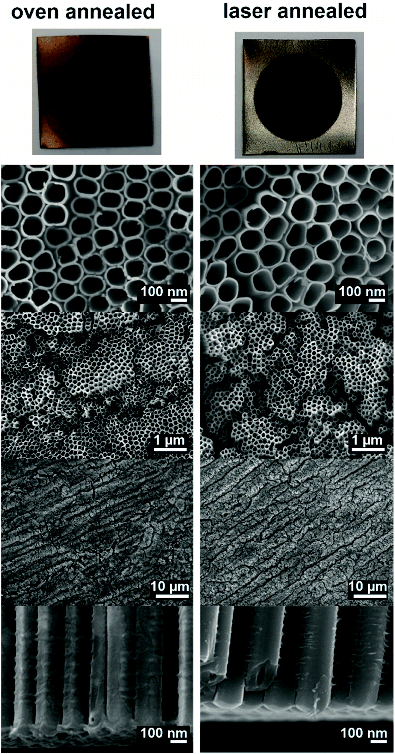 | ||
| Fig. 1 Photographs and SEM images of different magnifications of the oven and the laser annealed samples. | ||
The SEM images in Fig. 1 show clearly, that the TNTs themselves were not molten, ablated or deformed during the laser treatment. This is due to the optimized laser treatment conditions used herein, in contrast to previously published studies on laser annealing of TNT layers.44–47 When a higher energy density (>1.1 mJ cm−2) of the laser or a slower scanning velocity (providing more than 106 laser shots per irradiation site at ∼1 mJ cm−2) were applied, the TNT layers deformed or even melted on the top.
Fig. 2a shows the XRD pattern of the laser and the oven annealed TNT layer. As one can see, for both samples the typical diffraction signals for anatase were obtained while no signals for rutile phase were visible. The laser annealed TNT layer revealed lower signals and a higher background, thus a lower crystallinity compared to the oven annealed TNT layer which was exposed to high temperatures for several hours. The crystallite size of both TNT layers was calculated using Scherrer's equation56 as 456 Å and 583 Å for the laser annealed and the oven annealed TNT layer, respectively. The diffraction signals of Ti visible in the XRD patterns of both samples stem from the underlying Ti foil.
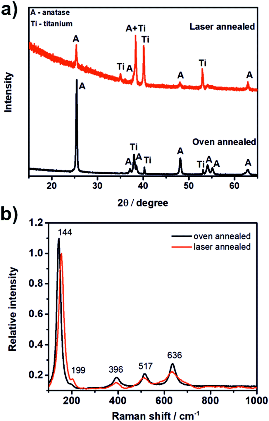 | ||
| Fig. 2 XRD pattern (a) and normalized Raman spectra (b) of the laser and the oven annealed samples. | ||
Fig. 2b shows the Raman spectrum of the laser annealed sample. According to the literature57 anatase shows six Raman active modes: A1g (519 cm−1), 2B1g (399 cm−1 and 519 cm−1) and 3Eg (144 cm−1, 197 cm−1, and 639 cm−1). Thus, in total five peaks are expected in the Raman spectrum as the signals of the A1g and one B1g mode appear at the same position. All five peaks can be seen in the Raman spectrum of the laser annealed sample (Fig. 2b) and confirm that the prior amorphous TNT layer was successfully transferred into anatase phase by laser annealing. The slight peak shifts that were found compared to the values given in the literature, i.e. for the signal at 144 cm−1, can be attributed to three different reasons: (i) in case of TiO2 nanoparticles the peak at 144 cm−1 shows a strong dependence on the sample nanostructure and dimensions and has been attributed to quantum confinement effects;57 (ii) a difference in the stoichiometry of TiO2;57 and (iii) a difference in the crystallite size.58
For a deeper investigation of the crystallinity of the laser annealed nanotube layers, HRTEM imaging with use of fast Fourier transformation (FFT) analysis of the TNT structure was carried out (Fig. 3). Within a sample of one TNT layer, essentially three different morphologies of TNT structure were found: (1) fully crystalline nanotubes with a single crystal structure of the walls, (2) fully amorphous nanotubes, and (3) partly crystalline nanotubes, having an amorphous structure containing many nano-crystals with different orientations maybe showing early stages of the nanotube crystallization. This confirms the assumption from the XRD results in Fig. 2a that the laser annealing leads to a lower degree of crystallinity than the oven annealing. This is similarly to other reports in the literature on laser annealing of TNT layers.44,47,48 A reason for the lower degree of crystallinity of the laser annealed samples is most likely a non-homogenous laser irradiation during scanning, possibly due to the fact that the laser has about 8–10% instability (e.g. in pulse energy).
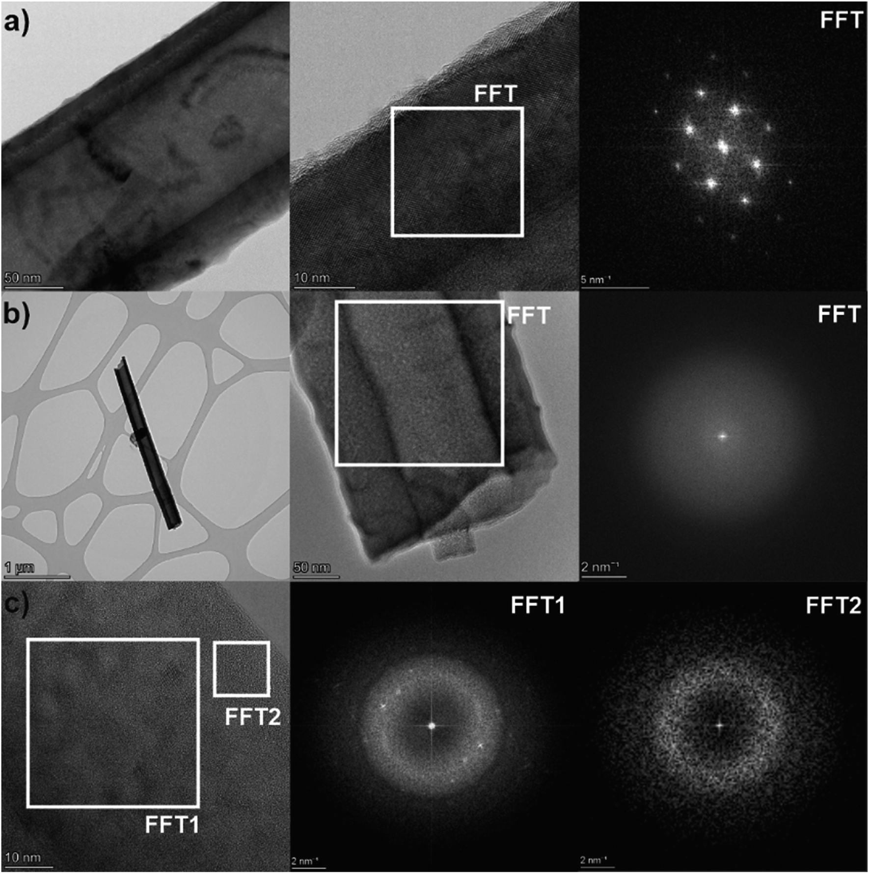 | ||
| Fig. 3 HR-TEM images and related FFT patterns for (a) fully crystalline, (b) fully amorphous, and (c) partly crystalline nanotubes (where FFT1 reveals a mixture of many nano-crystals with different orientation and amorphous structure) in the laser annealed TNT layer. | ||
XPS analyses of laser and oven annealed samples are shown in Fig. 4a–f. Both survey spectra (Fig. 4a and b) reveal the presence of C, O, Ti, however the laser annealed sample has F stemming from the electrolyte. The fact that no F was detected for the oven annealed sample may be attributed to the long duration of dwell of the sample in the oven. During this time, the amount of C and F species is reduced by the formation of volatile compounds.22 The Ti 2p spectrum of the laser annealed sample (Fig. 4c) was decomposed in six contributions corresponding to three different chemical environments. Peaks obtained at 459.1 and 464.8 eV were attributed to Ti4+, that is TiO2.59–61 Signals at 457.9 and 463.6 eV were associated with Ti3+.60,61 Finally, contributions to 460.1 and 465.8 eV were assigned to Ti–F.61 The Ti 2p signal of the oven annealed sample (Fig. 3d) also has three chemical species, Ti4+ with the doublets centred at 458.7 and 464.4 eV, Ti3+ at 457.5 and 463.2 eV and non-stoichiometric titanium oxide, TiOx, at 459.6 and 465.3 eV.62 O 1s spectra of the laser and oven annealed (Fig. 4e and f) samples displayed the same four chemical species. The signals at 530.3 and 530.0 eV, respectively, correspond to oxygen bond with titanium, Ti–O (TiO2).59–61 The Ti bonding with hydroxyl bridge groups (Ti–OHB) appears at 531.3 and 531.2 eV.63–65 Peaks at 532.2 and 532.1 eV were assigned to Ti bonding with hydroxyl terminal group (Ti–OHT)63–65 And the signals at 533.2 and 533.1 eV were associated to carboxyl group, (C![[double bond, length as m-dash]](https://www.rsc.org/images/entities/char_e001.gif) O)–OH.59,66 The chemical shifting, evident in the common titanium and oxygen species in the samples, could be due to the presence of F in the laser annealed sample, which generates a change in the electronic cloud of these elements. XPS measurements were also used to confirm the stoichiometry of the TiO2; the results of composition are summarized in Table 1. The stoichiometry of the samples can be calculated by the ratio of the concentrations of the Ti bonded to O (Ti–O) and Ti4+ resulting in ratios of 2.08
O)–OH.59,66 The chemical shifting, evident in the common titanium and oxygen species in the samples, could be due to the presence of F in the laser annealed sample, which generates a change in the electronic cloud of these elements. XPS measurements were also used to confirm the stoichiometry of the TiO2; the results of composition are summarized in Table 1. The stoichiometry of the samples can be calculated by the ratio of the concentrations of the Ti bonded to O (Ti–O) and Ti4+ resulting in ratios of 2.08![[thin space (1/6-em)]](https://www.rsc.org/images/entities/char_2009.gif) :1 (O:Ti) and 2.313:1 (O:Ti) for the laser annealed and the oven annealed TNT layers, respectively, meaning, the stoichiometry of the laser annealed TNT layer is better than of the oven annealed TNT layer. Thus, the Raman peak shifts are probably connected with the differences in crystallite size.
:1 (O:Ti) and 2.313:1 (O:Ti) for the laser annealed and the oven annealed TNT layers, respectively, meaning, the stoichiometry of the laser annealed TNT layer is better than of the oven annealed TNT layer. Thus, the Raman peak shifts are probably connected with the differences in crystallite size.
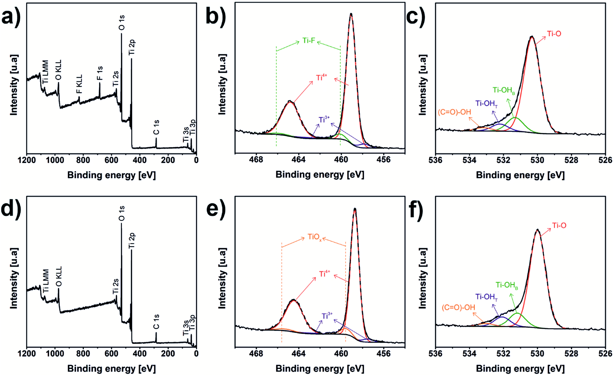 | ||
| Fig. 4 XPS spectra of laser (a–c) and oven (d–f) annealed samples: (a and d) survey, (b and e) Ti 2p, and (c and f) O 1s spectra. | ||
O)–OH is the carboxyl-group, Ti–F is the bonding between Ti and F. TiOx is non-stoichiometric TiO2
| Sample | Atomic concentration [%] | |||||||||
|---|---|---|---|---|---|---|---|---|---|---|
| C | F | Ti–O | Ti–OHB | Ti–OHT | (CO)–OH |
Ti4+ | Ti3+ | Ti–F | TiOx | |
| Laser annealed | 17.19 | 6.97 | 42.00 | 6.13 | 3.12 | 1.49 | 20.21 | 0.69 | 0.90 | — |
| Oven annealed | 19.64 | — | 46.15 | 6.45 | 4.53 | 1.45 | 20.01 | 0.60 | — | 1.16 |
Fig. 5a and b show the incident photon-to-electron conversion efficiency (IPCE) and the photocurrent density transients for the laser and the oven annealed TNT layers. As one can see, a strong increase of the IPCE and the photocurrent density was recorded for the oven annealed TNT layer with a photocurrent density maximum at a wavelength of ∼360 nm. Compared to the oven annealed TNT layer the laser annealed TNT layer revealed significantly lower IPCE values and photocurrent densities with a photocurrent density maximum at a wavelength of ∼320 nm. This means that the recombination rate of the charge carriers is much higher in case of the laser annealed TNT layer, thus it contains more defects. This can be confirmed by the majority carrier concentration (ND) calculated from the Mott–Schottky plots (Fig. 5c)16,18 which is significantly increased for the laser annealed TNT layer (i.e. 6.21 × 1020 cm−3 vs. 4.73 × 1019 cm−3 for the laser and the oven annealed TNT layer, respectively). By extrapolation of the linear part of the Mott–Schottky plots to 1/C2 = 0 the flatband potential Efb of the TNT layers can be calculated and results in −0.18 V for the laser annealed and +0.26 V for the oven annealed TNT layer. This significant cathodic shift of Efb for the laser annealed TNT layer could be explained by specific ion adsorption form the electrolyte due to the surface states67 or by a higher density of defects in the nanotube walls. In general, the higher ND and the lower Efb indicate a higher conductivity of the laser annealed TNT layer, as shown in the literature for Ti3+ self-doped TNT layers.68,69 Another reason for the higher conductivity of the laser annealed TNT layers is the absence of the thermal oxide layer between the TNTs and the Ti substrate which can be found for oven annealed samples (Fig. 1).20,34,35 Finally, Fig. 5d shows linear scan volatmmograms recorded on both samples in the dark at a low sweep rate of 5 mV s−1. As one can see, the onset potential for the hydrogen evolution reaction is shifted towards a more positive potential for the laser annealed TNT layers compared to the oven annealed one (i.e. ca. −0.45 V for the laser annealed TNT layer and ca. −0.6 V for the oven annealed layer), thus showing an improved overpotential for hydrogen evolution. However, the calculated Tafel slopes, as shown in the inset of Fig. 5d, show faster kinetics for the oven annealed TNT layer than for the laser annealed TNT layer. A reason for this could be that the laser annealed TNT layers are not fully crystalline.
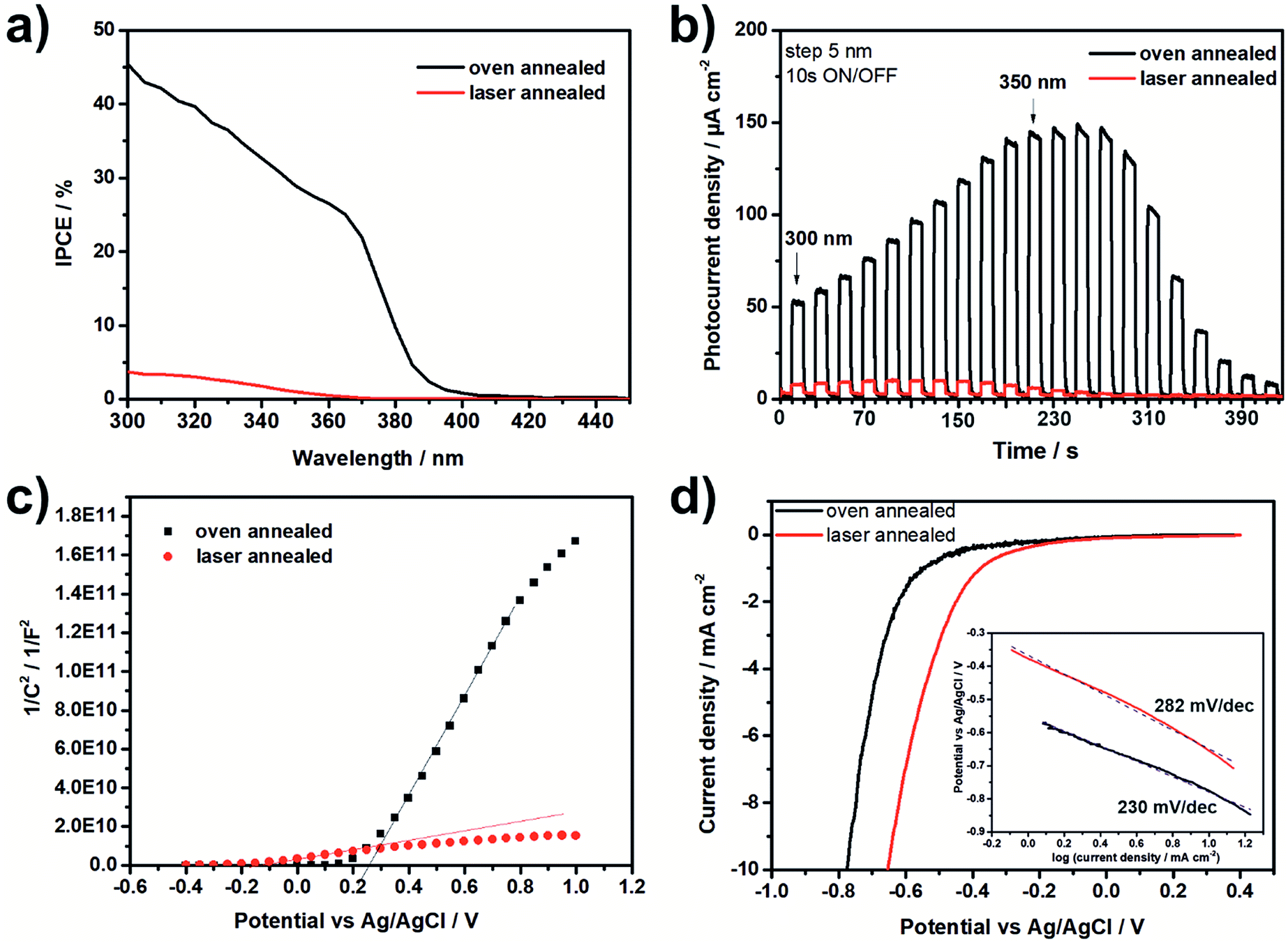 | ||
| Fig. 5 IPCE vs. wavelength (a), photocurrent density transients recorded at wavelength between 300 nm and 400 nm with a step of 5 nm (b), Mott–Schottky plots recorded at a frequency of 1 kHz in the voltage range between 1 V and −0.4 V (c) and linear sweep voltammograms recorded in the dark at a sweep rate of 5 mV s−1 for the laser and the oven annealed TNT layers (d). The inset in (d) shows the calculated Tafel slopes. All measurements were carried out in 1 M HClO4. | ||
Conclusions
In conclusion, the successful annealing of TNT layers by means of a picosecond laser treatment under optimised processing conditions was shown. SEM investigations of the laser annealed TNT layers revealed that the tops of the layers did not show any differences in comparison to conventional oven annealed TNT layers. No melting or deformation of the TNTs was observed for the first time. Furthermore, the conversion of the as-prepared amorphous TNT layers to anatase phase was confirmed by XRD and Raman spectroscopy. However, extensive HRTEM investigation of the laser annealed TNT layers showed that it consists of fully crystalline, fully amorphous and partly crystalline nanotubes. XPS spectra show a better surface stoichiometry of the laser annealed samples compared to their oven annealed counterparts. (Photo-)electrochemical measurements reveal that the laser annealed TNT layers contain more defects than the oven annealed TNT layers, resulting in lower photocurrent densities, a lower flatband potential and higher donor concentration. However, a lower overportential for hydrogen evolution reaction was observed for the laser annealed TNT layer.Conflicts of interest
There are no conflicts to declare.Acknowledgements
European Research Council (No. 638857) and the Ministry of Education, Youth and Sports of the Czech Republic (LM2018103, LO1411, LQ1601) are acknowledged for financial support of this work. CzechNanoLab project (LM2018110) is acknowledged for the financial support of the TEM measurements at CEITEC Nano Research Infrastructure. The HiLASE team acknowledges the European Regional Development Fund and the state budget of the Czech Republic (Project HiLASE CoE, No. CZ.02.1.01/0.0/0.0/15_006/0000674; Project BIATRI, No. Project BIATRI: Grant No. CZ.02.1.01/0.0/0.0/15_003/0000445).Notes and references
- M. Assefpour-Dezfuly, C. Vlachos and E. H. Andrews, J. Mater. Sci., 1984, 19, 3626–3639 CrossRef CAS.
- V. Zwilling, E. Darque-Ceretti, A. Boutry-Forveille, D. David, M. Y. Perrin and M. Aucouturier, Surf. Interface Anal., 1999, 27, 629–637 CrossRef CAS.
- J. M. Macák, H. Tsuchiya, A. Ghicov and P. Schmuki, Electrochem. Commun., 2005, 7, 1133–1137 CrossRef.
- K. Zhu, N. R. Neale, A. Miedaner and A. J. Frank, Nano Lett., 2007, 7, 69–74 CrossRef CAS PubMed.
- P. Roy, D. Kim, K. Lee, E. Spiecker and P. Schmuki, Nanoscale, 2010, 2, 45–59 RSC.
- H. F. Lu, F. Li, G. Liu, Z.-G. Chen, D.-W. Wang, H.-T. Fang, G. Q. Lu, Z. H. Jiang and H.-M. Cheng, Nanotechnology, 2008, 19, 405504 CrossRef PubMed.
- R. Lü, W. Zhou, K. Shi, Y. Yang, L. Wang, K. Pan, C. Tian, Z. Ren and H. Fu, Nanoscale, 2013, 5, 8569 RSC.
- S. Ng, P. Kuberský, M. Krbal, J. Prikryl, V. Gärtnerová, D. Moravcová, H. Sopha, R. Zazpe, F. K. Yam, A. Jäger, L. Hromádko, L. Beneš, A. Hamáček and J. M. Macak, Adv. Eng. Mater., 2018, 20, 1700589 CrossRef.
- J. M. Macak, M. Zlamal, J. Krysa and P. Schmuki, Small, 2007, 3, 300–304 CrossRef CAS PubMed.
- Z. Liu, X. Zhang, S. Nishimoto, T. Murakami and A. Fujishima, Environ. Sci. Technol., 2008, 42, 8547–8551 CrossRef CAS PubMed.
- H. Sopha, M. Baudys, M. Krbal, R. Zazpe, J. Prikryl, J. Krysa and J. M. Macak, Electrochem. Commun., 2018, 97, 91–95 CrossRef CAS.
- J. H. Park, S. Kim and A. J. Bard, Nano Lett., 2006, 6, 24–28 CrossRef CAS PubMed.
- N. Liu, C. Schneider, D. Freitag, M. Hartmann, U. Venkatesan, J. Müller, E. Spiecker and P. Schmuki, Nano Lett., 2014, 14, 3309–3313 CrossRef CAS.
- J. M. Macak, H. Tsuchiya, A. Ghicov, K. Yasuda, R. Hahn, S. Bauer and P. Schmuki, Curr. Opin. Solid State Mater. Sci., 2007, 11, 3–18 CrossRef CAS.
- K. Lee, A. Mazare and P. Schmuki, Chem. Rev., 2014, 114, 9385–9454 CrossRef CAS PubMed.
- H. Tsuchiya, J. M. Macak, A. Ghicov, A. S. Räder, L. Taveira and P. Schmuki, Corros. Sci., 2007, 49, 203–210 CrossRef CAS.
- P. Roy, S. Berger and P. Schmuki, Angew. Chem., Int. Ed., 2011, 50, 2904–2939 CrossRef CAS PubMed.
- M. Krbal, H. Sopha, D. Pohl, L. Benes, C. Damm, B. Rellinghaus, J. Kupčík, P. Bezdička, J. Šubrt and J. M. Macak, Electrochim. Acta, 2018, 264, 393–399 CrossRef CAS.
- D. Regonini, A. Jaroenworaluck, R. Stevens and C. R. Bowen, Surf. Interface Anal., 2010, 42, 139–144 CrossRef CAS.
- S. Das, R. Zazpe, J. Prikryl, P. Knotek, M. Krbal, H. Sopha, V. Podzemna and J. M. Macak, Electrochim. Acta, 2016, 213, 452–459 CrossRef CAS.
- R. Zazpe, J. Prikryl, V. Gärtnerova, K. Nechvilova, L. Benes, L. Strizik, A. Jäger, M. Bosund, H. Sopha and J. M. Macak, Langmuir, 2017, 33, 3208–3216 CrossRef CAS PubMed.
- S. P. Albu, A. Ghicov, S. Aldabergenova, P. Drechsel, D. LeClere, G. E. Thompson, J. M. Macak and P. Schmuki, Adv. Mater., 2008, 20, 4135–4139 CAS.
- K. Shankar, M. Paulose, G. K. Mor, O. K. Varghese and C. A. Grimes, J. Phys. D: Appl. Phys., 2005, 38, 3543–3549 CrossRef CAS.
- C. Xu, Y. A. Shaban, W. B. Ingler and S. U. M. Khan, Sol. Energy Mater. Sol. Cells, 2007, 91, 938–943 CrossRef CAS.
- A. Mazare, I. Paramasivam, F. Schmidt-Stein, K. Lee, I. Demetrescu and P. Schmuki, Electrochim. Acta, 2012, 66, 12–21 CrossRef CAS.
- D. Wang, L. Liu, F. Zhang, K. Tao, E. Pippel and K. Domen, Nano Lett., 2011, 11, 3649–3655 CrossRef CAS PubMed.
- N. Liu, S. P. Albu, K. Lee, S. So and P. Schmuki, Electrochim. Acta, 2012, 82, 98–102 CrossRef CAS.
- S. Ng, H. Sopha, R. Zazpe, Z. Spotz, V. Bijalwan, F. Dvorak, L. Hromadko, J. Prikryl and J. M. Macak, Front. Chem., 2019, 7, 38 CrossRef CAS PubMed.
- A. Kirkey, J. Li and T. K. Sham, Surf. Sci., 2019, 680, 68–74 CrossRef CAS.
- J. Yu, G. Dai and B. Cheng, J. Phys. Chem. C, 2010, 114, 19378–19385 CrossRef CAS.
- M. Benčina, I. Junkar, R. Zaplotnik, M. Valant, A. Iglič and M. Mozetič, Materials, 2019, 12, 626 CrossRef PubMed.
- J. M. Aquino, R. C. Rocha-Filho, N. Bocchi and S. R. Biaggio, Mater. Lett., 2014, 126, 52–54 CrossRef CAS.
- J. M. Aquino, J. P. Silva, R. C. Rocha-Filho, S. R. Biaggio and N. Bocchi, Mater. Lett., 2016, 167, 209–212 CrossRef CAS.
- A. Ghicov, H. Tsuchiya, J. M. Macak and P. Schmuki, Phys. Status Solidi A, 2006, 203, 28–30 CrossRef.
- S. P. Albu, H. Tsuchiya, S. Fujimoto and P. Schmuki, Eur. J. Inorg. Chem., 2010, 4351–4356 CrossRef CAS.
- O. Van Overschelde, R. Snyders and M. Wautelet, Appl. Surf. Sci., 2007, 254, 971–974 CrossRef CAS.
- O. Van Overschelde, G. Guisbiers, F. Hamadi, A. Hemberg, R. Snyders and M. Wautelet, J. Appl. Phys., 2008, 104, 103106 CrossRef.
- W.-T. Hsiao, C.-C. Yang, S.-F. Tseng, D. Chiang, K.-C. Huang, K.-M. Lin and M.-F. Chen, Appl. Phys. A, 2016, 122, 381 CrossRef.
- J. S. Hoppius, D. Bialuschewski, S. Mathur, A. Ostendorf and E. L. Gurevich, Appl. Phys. Lett., 2018, 113, 071904 CrossRef.
- K. Wesang, A. Hohnholz, R. Jahn, S. Steenhusen and P. Löbmann, Lasers Manuf. Mater. Process, 2019, 6, 387–397 CrossRef.
- L. F. Gerlein, J. A. Benavides-Guerrero and S. G. Cloutier, Adv. Eng. Mater., 2020, 22, 1901014 CrossRef CAS.
- Y. Joya and Z. Liu, Scr. Mater., 2009, 60, 467–470 CrossRef CAS.
- V. Likodimos, T. Stergiopoulos, P. Falaras, J. Kunze and P. Schmuki, J. Phys. Chem. C, 2008, 112, 12687–12696 CrossRef CAS.
- M. Y. Hsu, N. Van Thang, C. Wang and J. Leu, Thin Solid Films, 2012, 520, 3593–3599 CrossRef CAS.
- M. Enachi, A. Sarua, M. Stevens-Kalceff, I. Tiginyanu, L. Ghimpu and V. Ursaki, J. Appl. Phys., 2013, 234302 CrossRef.
- K. Siuzdak, M. Szkoda, M. Sawczak, J. Karczewski, J. Ryl and A. Cenian, Thin Solid Films, 2018, 659, 48–56 CrossRef CAS.
- J. Wawrzyniak, J. Karczewski, P. Kupracz, K. Grochowska, K. Załęski, O. Pshyk, E. Coy, M. Bartmański, M. Szkodo and K. Siuzdak, Appl. Surf. Sci., 2020, 508, 145143 CrossRef.
- Ł. Haryński, K. Grochowska, P. Kupracz, J. Karczewski, E. Coy and K. Siuzdak, Nanomaterials, 2020, 10, 430 CrossRef PubMed.
- Y. Xu, M. A. Melia, L. Tsui, J. M. Fitz-Gerald and G. Zangari, J. Phys. Chem. C, 2017, 121, 17121–17128 CrossRef CAS.
- Ł. Haryński, K. Grochowska, J. Karczewski, J. Ryl and K. Siuzdak, ACS Appl. Mater. Interfaces, 2020, 12, 3225–3235 CrossRef PubMed.
- R. Zazpe, M. Knaut, H. Sopha, L. Hromadko, M. Albert, J. Prikryl, V. Gärtnerová, J. W. Bartha and J. M. Macak, Langmuir, 2016, 32, 10551–10558 CrossRef CAS PubMed.
- O. Novák, H. Turčičová, M. Smrž, T. Miura, A. Endo and T. Mocek, Opt. Lett., 2016, 41, 5210 CrossRef PubMed.
- H. Turcicova, O. Novak, L. Roskot, M. Smrz, J. Muzik, M. Chyla, A. Endo and T. Mocek, Opt. Express, 2019, 27, 24286 CrossRef CAS PubMed.
- S. Das, H. Sopha, M. Krbal, R. Zazpe, V. Podzemna, J. Prikryl and J. M. Macak, ChemElectroChem, 2017, 4, 495–499 CrossRef CAS PubMed.
- M. Motola, L. Hromadko, J. Přikryl, H. Sopha, M. Krbal and J. M. Macak, Electrochim. Acta, 2020, 352, 136479 CrossRef CAS.
- J. I. Langford and A. J. C. Wilson, J. Appl. Crystallogr., 1978, 11, 102–113 CrossRef CAS.
- A. Li Bassi, D. Cattaneo, V. Russo, C. E. Bottani, E. Barborini, T. Mazza, P. Piseri, P. Milani, F. O. Ernst, K. Wegner and S. E. Pratsinis, J. Appl. Phys., 2005, 98, 074305 CrossRef.
- W. F. Zhang, Y. L. He, M. S. Zhang, Z. Yin and Q. Chen, J. Phys. D: Appl. Phys., 2000, 33, 912–916 CrossRef CAS.
- J. F. Moulder, W. F. Stickle, P. E. Sobol and K. D. Bomben, Handbook of X-ray Photoelectron Spectroscopy, Physical Electronics, Inc., 1995 Search PubMed.
- L. J. Hoyos, D. F. Rivera, A. F. Gualdrón-Reyes, R. Ospina, J. Rodríguez-Pereira, J. L. Ropero-Vega and M. E. Niño-Gómez, Appl. Surf. Sci., 2017, 423, 917–926 CrossRef CAS.
- A. F. Gualdrón-Reyes, A. M. Meléndez, M. A. Mejía-Escobar, F. Jaramillo and M. E. Niño-Gómez, New J. Chem., 2018, 42, 14481–14492 RSC.
- C. Ocal and S. Ferrer, Surf. Sci., 1987, 191, 147–156 CrossRef CAS.
- H. Maeda, T. Kasuga and M. Nogami, J. Eur. Ceram. Soc., 2004, 24, 2125–2130 CrossRef CAS.
- C.-Y. Wu, K.-J. Tu, J.-P. Deng, Y.-S. Lo and C.-H. Wu, Materials, 2017, 10, 566 CrossRef PubMed.
- P. Krishnan, M. Liu, P. A. Itty, Z. Liu, V. Rheinheimer, M.-H. Zhang, P. J. M. Monteiro and L. E. Yu, Sci. Rep., 2017, 7, 43298 CrossRef PubMed.
- P. G. Rouxhet and M. J. Genet, Surf. Interface Anal., 2011, 43, 1453–1470 CrossRef CAS.
- A. J. Bard, F.-R. F. Fan, A. S. Gioda, G. Nagasubramanian and H. S. White, Faraday Discuss. Chem. Soc., 1980, 70, 19–31 RSC.
- J. Song, M. Zheng, X. Yuan, Q. Li, F. Wang, L. Ma, Y. You, S. Liu, P. Liu, D. Jiang, L. Ma and W. Shen, J. Mater. Sci., 2017, 52, 6976–6986 CrossRef CAS.
- Q. Kang, J. Cao, Y. Zhang, L. Liu, H. Xu and J. Ye, J. Mater. Chem. A, 2013, 1, 5766 RSC.
| This journal is © The Royal Society of Chemistry 2020 |