
 Open Access Article
 This Open Access Article is licensed under a Creative Commons Attribution-Non Commercial 3.0 Unported Licence
Identification of the local electrical properties of crystalline and amorphous domains in electrochemically doped conjugated polymer thin films†
Hemanth Maddalia,
Krystal L. Housea,
Thomas J. Emgea and
Deirdre M. O'Carroll *ab
*ab
aDepartment of Chemistry and Chemical Biology, Rutgers University, 610 Taylor Road., Piscataway, NJ 08854, USA. E-mail: ocarroll@rutgers.edu
bDepartment of Materials Science and Engineering, Rutgers University, 607 Taylor Rd., Piscataway, NJ 08854, USA
First published on 5th June 2020
Abstract
Doped polymer thin films have several applications in electronic, optoelectronic and thermoelectric devices. Often the electrical properties of doped conjugated polymer thin films are affected by their local physical and mechanical characteristics. However, investigations into the effects of doping on local domain properties have not been carried out. Here, we study the physical, mechanical and optical properties of electrochemically doped P3HT thin films at the nanoscale and establish a relation between doping level and the physical properties of P3HT thin films. Bulk crystallinity of both pristine and doped P3HT thin films, characterized using grazing incidence X-ray diffraction, shows a clear loss in crystallinity upon doping. Nanoscale crystalline and amorphous domains in the films are visualized by multimode atomic force microscopy (AFM). It is apparent that the crystalline domains are most affected by doping and have a higher degree of doping compared to amorphous domains. This results in crystalline domains exhibiting superior electrical conductivity at a local level. These results are further supported by Raman mapping and elemental analysis of doped films. A direct relation is established between the physical, mechanical and electrical properties of doped P3HT thin films based on the AFM data. The findings demonstrate that higher dopant concentrations are found in crystalline domains compared to amorphous domains, which has not been shown before to the best of our knowledge. This study can be used to optimize the electronic properties of doped P3HT thin films for use in electronic and optoelectronic device applications.
Introduction
The discovery of conductivity in doped polyacetylene by Hideki Shirakawa, Alan MacDiarmid and Alan Heeger in 1977 resulted in great interest in the physics and chemistry of conjugated polymers.1,2 Conjugated polymers like polyacetylene, polypyrrole, polythiophene and polyaniline have been studied extensively in terms of their bulk optical and electrical properties due to their potential for various electronic and optoelectronic device applications.3 The alternating single and double bonds along these polymers result in excellent carrier mobilities making them intrinsic semiconductors. The ease of fabrication of these polymers into optoelectronic devices resulted in the reduction of cost as compared to their inorganic metal and semiconductor counterparts. Extensive investigations employing these polymers into low cost solar cells, light-emitting diodes, and thin film transistors have been performed in recent decades.4–7In recent years there has been renewed interest in molecular doping of conjugated polymers.8–13 Doping has improved the conductivity of these polymers by several orders of magnitude, thereby enhancing the efficiency of variety of devices like organic light-emitting diodes,14 solar cells15,16 and other electronic devices17,18 in which these polymers have been used. The electrical properties of these polymers can be fine-tuned using different molecules as dopants which can act as an active layer in organic thermoelectrics19 and organic field-effect transistors.19–22
Several studies have been performed recently in order to improve the electrical properties of these doped conjugated polymers.11–13,23–26 A significant number of those studies focused on improving the physical properties like crystallinity, alignment and orientation of the conjugated polymer films.13,25,27–29 These studies have shown that improving crystallinity of pristine and doped conjugated polymer thin films results in higher mobility of charge carriers and thus contributes to the electrical conductivity.30 A great deal of work has also been done to improve the level of doping, as high doping levels can be challenging to achieve without disrupting the morphology of the fabricated polymer films.31 Achieving high doping levels via chemical doping can be directly related to high charge carrier densities, which can then be related to higher electric conductivity. The mechanism of different types of doping has been extensively studied and many models were proposed in order to optimize the procedure of doping.32–37 These models predict the dopant sites in the films which enables for optimization of physical properties in order to maximize the presence of dopant in the film. However, knowledge of the relative distribution of dopant sites between the amorphous and crystalline domains in a conjugated polymer thin film is currently limited.
In this article, we characterize electrochemically doped poly(3-hexylthiophene) (P3HT) thin films using absorption and Raman spectroscopy, fast force mapping and conductive atomic force microscopy (CAFM). We evaluate and compare the nanoscale physical, mechanical and electrical properties of pristine P3HT and doped P3HT thin films that were characterized by using CAFM. A comparison of the physical and electrochemical properties of both pristine and doped P3HT films enables us to establish a relationship between their Young's modulus and their respective electrical conductivity. Domains with higher Young's modulus parameter, which are assumed to have higher crystallinity, have better electric conduction than domains with lower Young's modulus. Based on the Young's modulus parameters of doped films, a relationship between the doping levels in crystalline and amorphous domains down to the nanoscale is established. Upon examining Raman spectra, the relation between doping levels and the relative crystallinity of the film is confirmed. This article finally establishes a correlation between physical and electrical properties to the doping levels in P3HT films.
Materials and methods
Poly(3-hexylthiophene) regioregular (electronic grade MW = 55 K, PDI = 2.8) was purchased from Rieke Metals. A platinum counter electrode (part no. CHI115) and a Ag/Ag+ non-aqueous reference electrode (part no. CHI112) were obtained from CH Instruments. Chloroform (anhydrous, ≥99% purity), acetonitrile (anhydrous, 99.8% purity); tetrabutylammonium perchlorate (≥99% purity), and indium-tin-oxide (ITO) coated glass substrates (surface resistivity 70–100 Ω sq−1) were purchased from Sigma-Aldrich.Thin-film fabrication
ITO-on-glass substrates were pre-cleaned by sequential sonication in acetone, deionized water and isopropanol, each for 15–20 minutes. Then, the ITO substrates were treated with oxygen plasma for one minute in a plasma cleaner. Thin films were fabricated by dynamic spin coating ∼7 μL of a 20 mg ml−1 solution of regioregular P3HT in chloroform at 3000 rpm for one minute on the pre-cleaned ITO-on-glass substrates. Electrochemical doping was performed, after spin coating the P3HT film on an ITO substrate. A three electrode setup was employed with polymer-coated ITO-on-glass as the working electrode, platinum wire as the counter electrode and a non-aqueous (Ag/AgCl) reference electrode. Tetrabutylammonium perchlorate (TBAP) was used as an electrolyte cum dopant and acetonitrile was used as the solvent. Chronoamperometry was used with the voltage going from 0 V to 4 V in a duration of 1 s, staying at 4 V for 2 s, and then dropping down to 0 V (EZstat-pro potentiostat, NuVant Systems Inc.). Upon doping, these films were dipped in acetonitrile to remove any residual dopant from the surface of the film. These films were then dried in a vacuum oven for 3 hours until they were taken out for further analysis.UV-visible absorbance measurements
UV-visible absorbance spectroscopy measurements were performed using a S.I. Photonics CCD array spectrophotometer with deuterium and tungsten lamps. The minimum wavelength was set at 300 nm and the maximum was set at 800 nm with the lamp crossover wavelength being 360 nm, and the spectra were recorded with the ‘‘high precision’’ setting.Grazing incidence X-ray diffraction
Grazing incidence X-ray diffraction (XRD) data were obtained by use of a Bruker Vantec-500 area detector and a Bruker FR571 rotating-anode X-ray generator operating at 40 kV and 45 mA and equipped with a 3-circle Azlan goniometer. The system used 0.5 mm pinhole collimation and a Rigaku Osmic parallel-mode (e.g., primary beam dispersion less than 0.01 degrees in 2θ) mirror monochromator (Cu Kα; λ = 1.5418 Å). Data were collected at room temperature with a sample to detector distance of 10 cm. A blank (ITO-glass slide surface) was also collected and substrated from the P3HT and TBAP sample data. Data collection was carried out using Bruker GADDS v.4.1.51 (2015) software.Atomic force microscopy (AFM) analysis of thin films
The AFM study was done using an Asylum Research Cypher ES Atomic Force Microscope. The measurements were performed under ambient conditions in the sealed AFM enclosure to reduce noise at a set sample temperature of 25 °C. All parts in contact with the cantilever and sample were thoroughly cleaned before experiments with ethanol then dried with a flow of ultra-high purity nitrogen. Prior to use, each cantilever was cleaned in a UV ozone cleaner (Ossila E511, UK) for a minimum of five minutes to remove contaminants. Before each measurement the spring constant of each cantilever was determined using the thermal tune method,38 and the deflection sensitivity was measured against a sapphire surface.Topography and phase images were acquired by operating the AFM in amplitude modulation mode (also often referred to as “tapping mode” or “AC-mode”). Silicon cantilevers, HQ-300-Au (Asylum Research) and TAP300 (Ted Pella), were used each with a nominal spring constant of k = 40 Nm−1 and nominal tip radius of r < 10 nm. For topography, the scan size was typically 4 μm2. A digital resolution of 256 lines × 256 points and a scanning rate of 1.6 Hz were used. The oscillation frequency of the probe was set at or near resonance at 253 kHz. The spring constant of the tip was determined to be 25.26 Nm−1 using thermal tune method.
AFM nanomechanical mapping measurements were obtained in Fast Force Mapping mode (FFM). For FFM, silicon cantilevers, AC200TS (Asylum Research) were used with nominal spring constant of k = 9 Nm−1 and nominal tip radius of r = 7 nm. The actual spring constant of the cantilever was determined to be 1.68 Nm−1 using the thermal tune method.38 The scan size was typically 1 μm.2 A digital resolution of 256 lines × 512 points and a scanning rate of 100 Hz were used. The maximum force was typically set at 10–40 nN. The Young's modulus, E, was obtained by fitting the force curve using the Hertz model.39
Conductive AFM measurements (CAFM) were acquired either with silicon cantilevers with a Ti/Pt tip coating, AC240TM-R3 (Asylum Research), with a nominal spring constant of 2 Nm−1 and nominal tip radius of 15 nm; or with silicon cantilevers with a Ti/Ir tip coating, ASYELEC.01-R2 (Asylum Research), with a nominal spring constant of 2.8 Nm−1 and nominal tip radius of 25 nm. Conductive AFM measurements were performed using a Dual Gain ORCA™ Conductive AFM probe holder (Asylum Research). Current images were acquired simultaneously with nanomechanical data in Fast Force Mapping Mode, the scan size was typically 1 × 1 μm2. A digital resolution of 256 lines × 256 points and a scanning rate of 100 Hz were used. Electric contact was made with the sample using silver paint on ITO. A bias voltage was applied between the tip and the ITO substrate and current was measured by the tip in contact with the conducting polymer. Current–voltage (I–V) sweeps were performed at various points of the sample by sweeping the pristine sample bias from 0 to 10 V and the doped sample from 0 to 1 V, while the current was measured with the tip.
AFM mode schematics
The sample surface is split into grid of points and moved below the tip in a raster pattern during FFM as shown in Fig. 1a. To allow for faster acquisition time, the cantilever is driven sinusoidally between force curves at a frequency far below the resonance frequency as FFM is considered a contact mode technique. The deflection of the cantilever is measured as a function of tip-sample separation (z) at each point in x, y. Data acquired includes topography, adhesion, and mechanical properties. Using CAFM, a current map of the sample can simultaneously be measured while performing an FFM. Here, a bias voltage is applied to the sample and current is measured through the sample by a metal-coated tip. This is achieved through an operational amplifier which holds the tip at virtual ground. Using Kirchhoff's junction rule the current can be determined by dividing the voltage coming out of the transimpedance amplifier by the value of the gain resistor of the cantilever holder. Current–voltage sweeps were acquired at selected points on the sample (Fig. 1b). A bias voltage is applied to the sample while current is measured through the sample by the tip as previously described.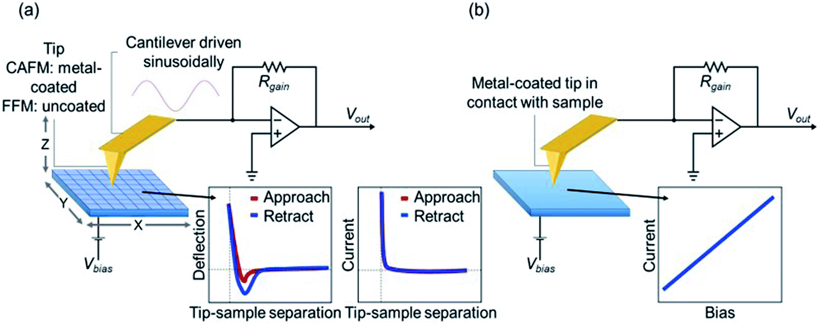 | ||
| Fig. 1 (a) Nanomechanical measurements and current images were performed in FFM mode. (b) Point I–V curves performed in contact mode. | ||
Raman spectroscopy
Raman spectroscopy was performed using a Raman microscope (inVia Reflex, Renishaw) equipped with a 532 nm laser and a 100× objective. A thermoelectrically cooled detector with a charged coupled device chip was employed as a detector (Renishaw). Raman mapping was performed across an area with a step size of 1 μm over 972 points. The acquired data were analyzed by a combination of Wire 4.4 software and MATLAB.Energy disperse X-ray spectroscopy
Energy dispersive X-ray spectroscopy (EDS) was performed using an Oxford-XmaX80 detector coupled to a Zeiss-Sigma Field-emission scanning electron microscope (FE-SEM). The elemental maps were obtained at an operating voltage of 5 kV.Results and discussion
In this study, we investigated the nanoscale physical, mechanical and electrical properties of P3HT and electrochemically doped P3HT thin films. Thin films were fabricated and doped using the materials shown in Fig. 2a. The fabricated P3HT thin films were doped electrochemically with TBAP for one second at 4 V; see Materials and methods. TBAP was used as the dopant as it is expected to lead to higher conductivities compared to other dopants. This is due to the higher basicity of perchlorate counterion compared to other counterions.40 The doped films showed a clear change in color i.e., dark purple to light blue (Fig. 2b) upon doping. We performed UV-visible absorption spectroscopy on both pristine and doped samples to verify that there was a change in electronic structure. The pristine sample exhibited π–π* absorption peaks at 565 nm and 570 nm,41 and a shoulder at 600 nm (Fig. 2c). The absorption spectra of doped P3HT films did not exhibit π–π* absorption peaks. Instead the absorption increased with wavelength throughout the visible region without reaching a well-defined absorption maximum. The spectra exhibited a red shifted broad peak at ∼800 nm (Fig. 2c), indicating the decrease in energy gaps between HOMO and LUMO energy levels, which is caused by doping.42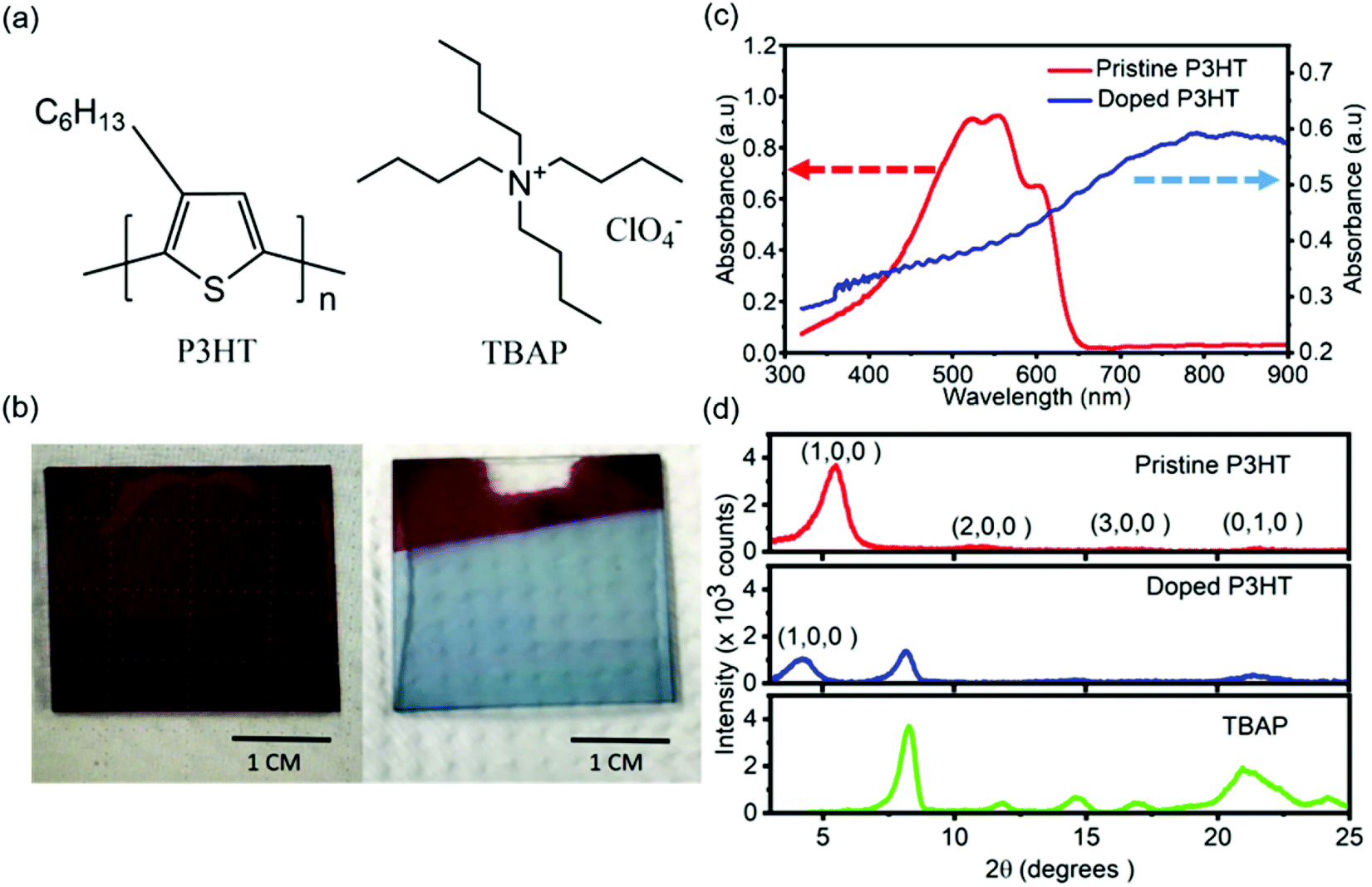 | ||
| Fig. 2 (a) Molecular structures of P3HT and the dopant TBAP. (b) Photographs of pristine (left) and electrochemically doped (right) P3HT on an ITO-on-glass substrate. (c) UV-visible absorption spectra of pristine and doped P3HT recorded on an ITO-on-glass substrate. (d) Grazing-incidence XRD measurements of pristine P3HT, doped P3HT and TBAP. | ||
In order to investigate bulk crystallinity of pristine and doped P3HT, grazing-incidence XRD was performed (Fig. 2d). Pristine P3HT exhibited a (1,0,0) diffraction peak at a 2θ value of ∼5.5° which can be attributed to a lamellar layered structure as a result of intermolecular alkyl chain stacking.43 Presence of (2,0,0), and (3,0,0) diffraction peaks along with the (1,0,0) peak indicate crystallinity along the alkyl chain stacking direction. The in-plane intermolecular π–π stacking peak, (0,1,0) was observed around 21.6°. For the doped film, the (1,0,0) peak shifted to a lower diffraction angle, 4.2°, while the (0,1,0) peak remained at a similar diffraction angle (21.4°) compared to the pristine film. This indicates an increase in the d-spacing in the alkyl chain stacking direction upon doping whereas, the d-spacing for the in plane π–π stacking remained similar. This confirms structural perturbations along the alkyl chain direction upon doping. The decrease in the intensity of the (1,0,0) crystalline peak from the pristine to the doped film indicates decreased crystallinity upon doping (Fig. S1†). Similar decreases in crystallinity were reported for doped P3HT in prior studies.44,45 The domain sizes were calculated (using the Scherrer equation) to be 6 nm and 11 nm for pristine and doped P3HT thin films, respectively. Therefore, although the crystallinity decreased, there is evidence for an increase in crystalline domain size upon electrochemical doping.
AFM analysis
Fig. 3 shows 5 μm × 5 μm topography and phase images of pristine P3HT and doped P3HT. The topography of both the films, as shown in Fig. 3a and b, exhibited a root mean square (RMS) roughness of 4.77 nm and 10.78 nm for pristine and doped P3HT, respectively. The increase in the roughness for the doped film can be attributed to the random localized cluster sites that are formed by dopant aggregation, during the doping process.31 Phase images provide a contrast between material properties, that cause phase shifts in the oscillations of the cantilever.46 Brighter spots in the phase images correspond to hard, more crystalline polymer, while darker areas represent soft, viscoelastic, amorphous polymer.47–49 The pristine film had regions of both crystalline and amorphous domains (Fig. 3c). The lower phase deflection for the brighter regions on the doped film, as shown in Fig. 3d, suggests a decrease in the inherent strength of the polymer. This could indicate alterations in the polymer packing due to the infusion of dopant molecules as a result of electrochemical doping. Also, the grain sizes in phase images were larger for the doped film, which could indicate more regions of harder domains (i.e., crystalline domains). Both pristine and doped films did not exhibit any correlation between their respective topography and phase images, indicating that the crystallinity of the polymer is independent of any changes in height.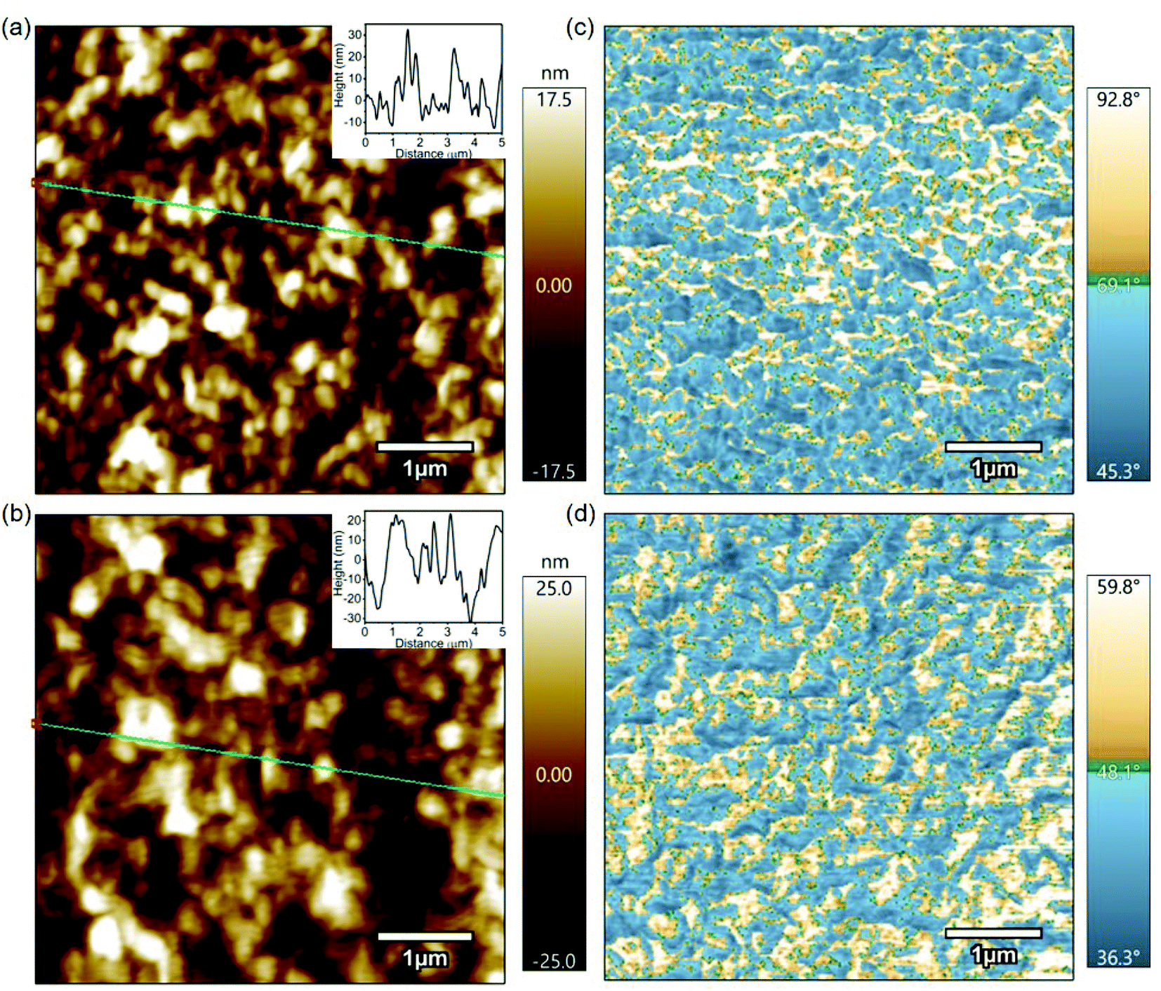 | ||
| Fig. 3 (a) and (b) 5 μm × 5 μm topography images of pristine and doped P3HT thin films, respectively. Insets show the height across the green lines. (c) and (d) 5 μm × 5 μm phase images of pristine and doped P3HT thin films, respectively. | ||
Hardness expressed in GPa is a good measure of a material's plastic behavior, just as modulus is a measure of a material's elastic response, and as such is directly related to the yield strength. Fast force mapping was performed on both pristine and doped P3HT films in order to evaluate the mechanical properties in terms of hardness and to generate a Young's modulus plot which indicates the strength of a material. These scans were higher in resolution compared to the topography scans. In these scans the Young's modulus parameter was calculated based on the Hertz model from the obtained hardness data. The Hertz model is not the most accurate model for estimating Young's modulus for conjugated polymers. But, we are more interested in the trend of FFM and current mapping scans for pristine and doped P3HT. Also, the Young's modulus map of both pristine and doped P3HT were not representative of their adhesion maps (Fig. S2†). The average Young's modulus for the pristine sample was ∼1.7 GPa, with the maximum being 2.34 GPa (Fig. 4c). Both of these values were closer to the theoretically estimated value i.e., 2.18 GPa.50 The doped sample exhibited an average Young's modulus of ∼1.1 GPa, with the maximum being 1.87 GPa (Fig. 4d). The domains with higher Young's modulus are considered to be more crystalline than the ones with lower Young's modulus, which are relatively amorphous in comparison. This reduction of the modulus from the pristine to the doped film indicates reduced strength of the film, although the total region of crystalline domain seems to have increased. Since crystalline domains in pristine films have a higher Young's modulus compared to the ones in doped films, this falls in line with the previous argument that was made above, regarding the decrease in inherent film hardness from the pristine to the doped film. The higher resolution phase images provided evidence of larger grain sizes for the doped film than the pristine film, as shown in Fig. 4a and b. There was a striking relation between the phase and the Young's modulus plot, as in, the crystalline regions suggested by the phase images have higher modulus when compared to the amorphous regions for both pristine and doped films. Histograms were plotted based on the data obtained from Young's modulus (Fig. 4e and f). These histograms were further evidence of the presence of two different domains with different modulus parameters. The peak at a higher Young's modulus corresponds to the more crystalline domains (harder) and the one at a lower Young's modulus corresponds to a more amorphous domain (softer). The amorphous peaks in both the pristine and the doped films were at 0.75 GPa whereas the crystalline peaks were around 1.6 GPa and 1.2 GPa for the pristine and doped films, respectively. This indicates that electrochemical doping affects only the crystalline domains of the polymer. We have established in the above discussions that infusion of dopant molecules in the polymer matrix decreases the inherent strength of the polymer. This can be used to explain a plausible situation in which the presence of dopants occur mostly in the crystalline domain of the conjugated polymer film. The better separation of Young's modulus peaks in doped P3HT film could be due to narrower, more homogeneous distributions of amorphous and crystalline regions. In other words, the amorphous and crystalline regions in doped P3HT film have better defined strength compared to the pristine one.
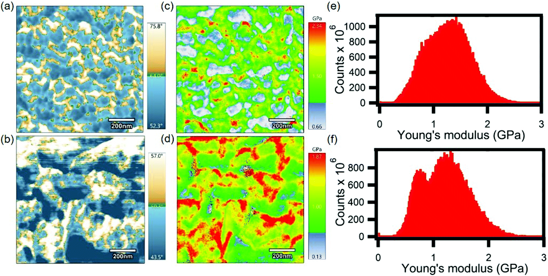 | ||
| Fig. 4 (a) and (b) 1 μm × 1 μm phase images of pristine and doped P3HT, respectively. (c) and (d) 1 μm × 1 μm Young's modulus images of pristine and doped P3HT, respectively. (e) and (f) Histograms representing all Young's modulus data points determined from AFM scans of pristine and doped P3HT, respectively. | ||
At the nanoscale, after confirming the presence of crystalline and amorphous domains in both pristine and doped P3HT, CAFM was performed in order to simultaneously measure the surface topography, Young's modulus and local electrical conductivity. A different tip with lower spring constant when compared to the ones used for FFM was employed for this measurement. The lower spring constant results in compression of the tip during indentation of the polymer, which explains the lower modulus values, as shown in Fig. 5a and b, as compared to those in FFM.51 The I–V curves of both pristine (top) and doped (bottom) P3HT exhibited linearity, as shown in Fig. S3,† which indicates the absence of turn on voltage in the circuit. The current in the electrochemically doped film was much higher (almost reaching to the higher limit of the apparatus) than the current in the pristine sample (Fig. 5e and f). Upon close examination of the current maps using a line scan, the regions with higher Young's modulus exhibited higher current values (Fig. 5e). This was more evident in the doped P3HT since there was higher current flowing through it when compared to the pristine one (Fig. 5f). Line scans were performed on these Young's modulus and current plots (Fig. S1†). These scans also provided further evidence that domains with higher Young's modulus conduct more current. Therefore, it can be deduced that the crystalline regions, which are expected to have a higher degree of order, conduct more electricity due to the higher extent of charge transfer43,52 and mobility than the amorphous regions. This provides evidence to the fact that, at the nanoscale level, the different domains in P3HT have unique physical, mechanical and electrical properties.
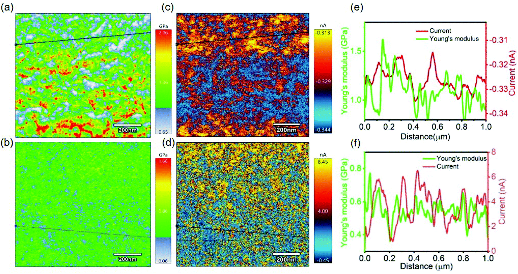 | ||
| Fig. 5 (a) and (b) 1 μm × 1 μm Young's modulus images of pristine and doped P3HT, respectively. (c) and (d and current, taken across the black lines shown) 1 μm × 1 μm current maps across the surface of pristine and doped P3HT, respectively. Applied voltages of 1 V and 0.5 V were used for (c) and (d), respectively. (e) and (f) show the Young's modulus and current, taken across the black lines shown in (a)–(d), for pristine and doped P3HT, respectively. | ||
Raman spectroscopy
Analyzing Raman spectra can be used to investigate the correlation between the degree of doping and crystallinity of P3HT films. Pristine P3HT thin films have a D band that corresponds to Cβ–Cβ intraring stretching vibrations at 1381 cm−1 (ref. 53) and a G band that corresponds to Cα = Cβ symmetric stretching vibrations at 1450 cm−1, as shown in Fig. 6a. The doped P3HT film had a slight shift in both the bands. The D band was observed at 1372 cm−1 and the G band was observed at 1435 cm−1 (Fig. 6b), indicating the presence of polarons and not bipolarons. This shifting in the wavenumbers can be attributed to the alteration in the length of π-delocalized structures.54 The full width half maximum (FWHM) of the G band is an indicator of degree of order in the film.55 The FWHM for the doped P3HT film (∼75 cm−1) was much higher than that of the pristine one (∼35 cm−1) indicating that the pristine film was more crystalline than the doped one. This was consistent with the above AFM data. In order to establish a correlation between doping intensity and the crystallinity for a doped sample, Raman mapping was performed. The FWHM of the G band over a certain number of points was calculated and plotted across the map (Fig. 6c). The FWHM values across the map ranged from ∼48 cm−1 to ∼56 cm−1. The map had areas of higher and lower degree of order since the FWHM was not constant. These areas were not as well resolved as the AFM force mapping images as the step size (1 μm) was around the size of different domains. The ratio of intensities of G band to D band were then calculated across the map and plotted as shown in Fig. 6d. This ratio was smaller for areas with higher doping concentrations.56–58 Correlating Fig. 6c and d we can establish that the areas of higher order contain higher doping concentrations which supports the concept that was established from the AFM data. For pristine films, no significant correlation was observed (Fig. S4†). | ||
| Fig. 6 (a) and (b) Raman spectra of pristine and doped P3HT films, respectively. (c) Plot of the FWHM of the G band across the mapped area of a doped P3HT film. (d) Plot of the ratio of the intensity of G band to the intensity of the D band across the mapped area of a doped P3HT film. | ||
Energy disperse X-ray spectroscopy
EDS was performed to identify the presence of sulfur from the polymer chain and chlorine from the dopant molecule and thereby to confirm the presence of TBAP dopant in the P3HT film. The EDS data across the surface of the thin films of sulfur (green) and chlorine (red) was displayed as a compositional map (Fig. 7a and b). Initially we performed a 1 μm × 1 μm scan in order to correlate this data to the AFM scans. The pristine films had a very minimal chlorine signal in a 1 μm × 1 μm map which was below the detector limit. In order to remedy this, a larger map (10 μm × 10 μm) area was scanned so that there was a signal above the detection limit. For the pristine P3HT thin films, the sulfur signal was much higher than that of chlorine as shown in Fig. 7a. This is due to the presence of sulfur in the thiophene rings of the polymer chain (Fig. 2a). This chlorine signal can be attributed to the trace amounts of the solvent (chloroform) from which the films were spin coated. This can be further evidenced from the EDS spectrum that shows a weak peak at 2.62 keV (Fig. 7c) which is the Kα energy of chlorine. The Kα energy of sulfur (2.31 keV) shows a peak much higher in intensity than that of chlorine as shown in Fig. 7c. The compositional map of doped P3HT film depicts a significantly higher chlorine signal at 2.62 keV compared to that of sulfur at 2.31 keV for a smaller map area (1 μm × 1 μm) as show in Fig. 7b. This significant increase in the presence of chlorine indicates a high level of doping by TBAP. The EDS spectrum was consistent with the compositional map by depicting higher chlorine counts compared to sulfur (Fig. 7d). The doped film was then dedoped by leaving the film in ambient conditions for 7 days. The EDS performed was similar to that of pristine film both in terms of compositional map and the EDS spectrum as shown in Fig. S5.†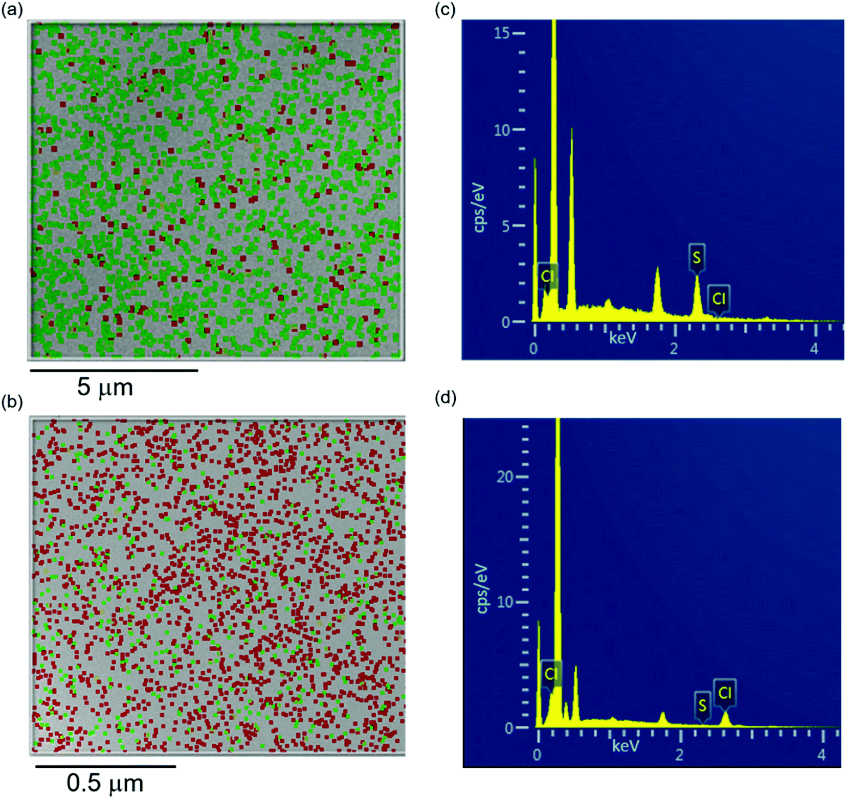 | ||
| Fig. 7 (a) and (b) Elemental compositional maps of both sulfur (green) and chlorine (red) on pristine and doped P3HT thin films, respectively. (c) and (d) EDS spectra of pristine and doped P3HT thin films, respectively. | ||
Conclusions
We have investigated the differences in the topography and composition of pristine and electrochemically doped P3HT thin films at the nanoscale. There was a clear loss of crystallinity from pristine to doped films upon doping which was evident in grazing-incidence XRD measurements. Pristine and doped P3HT thin films fabricated on ITO-coated glass substrates exhibited both crystalline and amorphous domains, as evidenced by AFM phase images. Fast force mapping measurements showed regions of higher and lower Young's modulus which confirmed the presence of crystalline and amorphous domains. Doping did not affect the amorphous domains, but the Young's modulus of crystalline domains decreased. This indicated the presence of dopants in the crystalline domains of the polymer. Current maps were simultaneously generated with fast force mapping. Comparing the pristine and doped current maps indicated that the doped sample exhibited current values which were about 30 times higher compared to the pristine sample. This indicates increase in electrical conductivity upon doping. Upon comparing the phase, fast force mapping and current maps of pristine samples, the crystalline domains exhibited higher current values indicating that crystalline domains exhibit higher conductivities. This was even more evident for the doped samples as they exhibited higher current values than the pristine samples. Raman mapping solidified the idea that crystalline domains have a higher dopant concentration when compared to the amorphous ones. Finally, by correlating phase images, Young's modulus plots, current maps, Raman maps, and EDS it is established that, upon electrochemical doping, the dopant sites preferentially occur in crystalline domains of the P3HT thin films and that the crystalline domains exhibit higher conductivities than amorphous ones. This work gives insight into how to modify electrical properties of doped conjugated polymer films at a nanoscale, with applications in organic electronic devices. Our concept also opens the way to various possibilities like maximizing the dopant levels in a polymer film by maximizing the percentage of crystalline domains. Also, the electrical properties can be tuned at the nanoscale level by altering the relative percentage of crystalline and amorphous domains.Conflicts of interest
There are no conflicts to declare.Acknowledgements
This work was supported, in part, by the National Science Foundation (grants DMR-1554954 and ECCS-1608389). We thank Dr Robert Hayes for useful discussions and assisting with AFM analysis. We are grateful to Dr Richard Haber, Mark Schaefer and Dr Berra Beyoglu-Siglam for access and training on SEM-EDS, Raman spectroscopy and mapping facilities. We are also thankful to Meghana Cyanam for her support with data analysis of Raman mapping.References
- H. Shirakawa, A. McDiarmid and A. Heeger, Chem. Commun., 2003, 1–4 RSC.
- H. Shirakawa, E. J. Louis, A. G. MacDiarmid, C. K. Chiang and A. J. Heeger, J. Chem. Soc., Chem. Commun., 1977, 578–580 RSC.
- T.-H. Le, Y. Kim and H. Yoon, Polymers, 2017, 9, 150 CrossRef PubMed.
- T. W. Kelley, P. F. Baude, C. Gerlach, D. E. Ender, D. Muyres, M. A. Haase, D. E. Vogel and S. D. Theiss, Chem. Mater., 2004, 16, 4413–4422 CrossRef CAS.
- A. C. Mayer, S. R. Scully, B. E. Hardin, M. W. Rowell and M. D. McGehee, Mater. Today, 2007, 10, 28–33 CrossRef CAS.
- J. Nelson, Science, 2001, 293, 1059 CrossRef CAS PubMed.
- H. Sirringhaus, N. Tessler and R. H. Friend, Science, 1998, 280, 1741 CrossRef CAS PubMed.
- P. Kar, Doping in conjugated polymers, John Wiley & Sons, 2013 Search PubMed.
- D. Gagnon, J. Capistran, F. Karasz, R. Lenz and S. Antoun, Polymer, 1987, 28, 567–573 CrossRef CAS.
- Y. Gao, H. L. Yip, K. S. Chen, K. M. O'Malley, O. Acton, Y. Sun, G. Ting, H. Chen and A. K. Y. Jen, Adv. Mater., 2011, 23, 1903–1908 CrossRef CAS PubMed.
- I. Salzmann, G. Heimel, M. Oehzelt, S. Winkler and N. Koch, Accounts Chem. Res., 2016, 49, 370–378 CrossRef CAS PubMed.
- R. A. Schlitz, F. G. Brunetti, A. M. Glaudell, P. L. Miller, M. A. Brady, C. J. Takacs, C. J. Hawker and M. L. Chabinyc, Adv. Mater., 2014, 26, 2825–2830 CrossRef CAS PubMed.
- K. H. Yim, G. L. Whiting, C. E. Murphy, J. J. Halls, J. H. Burroughes, R. H. Friend and J. S. Kim, Adv. Mater., 2008, 20, 3319–3324 CrossRef CAS.
- K. Walzer, B. Maennig, M. Pfeiffer and K. Leo, Chem. Rev., 2007, 107, 1233–1271 CrossRef CAS PubMed.
- L. Lu, T. Zheng, Q. Wu, A. M. Schneider, D. Zhao and L. Yu, Chem. Rev., 2015, 115, 12666–12731 CrossRef CAS PubMed.
- I. Salzmann and G. Heimel, J. Electron Spectrosc. Relat. Phenom., 2015, 204, 208–222 CrossRef CAS.
- G. Lu, J. Blakesley, S. Himmelberger, P. Pingel, J. Frisch, I. Lieberwirth, I. Salzmann, M. Oehzelt, R. Di Pietro and A. Salleo, Nat. Commun., 2013, 4, 1588 CrossRef PubMed.
- B. Lüssem, M. L. Tietze, H. Kleemann, C. Hoßbach, J. W. Bartha, A. Zakhidov and K. Leo, Nat. Commun., 2013, 4, 2775 CrossRef PubMed.
- B. Russ, A. Glaudell, J. J. Urban, M. L. Chabinyc and R. A. Segalman, Nat. Rev. Mater., 2016, 1, 16050 CrossRef CAS.
- H. H. Fong, V. A. Pozdin, A. Amassian, G. G. Malliaras, D.-M. Smilgies, M. He, S. Gasper, F. Zhang and M. Sorensen, J. Am. Chem. Soc., 2008, 130, 13202–13203 CrossRef CAS PubMed.
- B. S. Ong, Y. Wu, P. Liu and S. Gardner, J. Am. Chem. Soc., 2004, 126, 3378–3379 CrossRef CAS PubMed.
- H. Sirringhaus, N. Tessler and R. H. Friend, Science, 1998, 280, 1741–1744 CrossRef CAS PubMed.
- N. A. Ogurtsov, V. N. Bliznyuk, A. V. Mamykin, O. L. Kukla, Y. P. Piryatinski and A. A. Pud, Phys. Chem. Chem. Phys., 2018, 20, 6450–6461 RSC.
- E. M. Thomas, E. C. Davidson, R. Katsumata, R. A. Segalman and M. L. Chabinyc, ACS Macro Lett., 2018, 7, 1492–1497 CrossRef CAS.
- C. Y. Yang, W. L. Jin, J. Wang, Y. F. Ding, S. Nong, K. Shi, Y. Lu, Y. Z. Dai, F. D. Zhuang and T. Lei, Adv. Mater., 2018, 30, 1802850 CrossRef PubMed.
- Z. Liang, Y. Zhang, M. Souri, X. Luo, A. M. Boehm, R. Li, Y. Zhang, T. Wang, D.-Y. Kim and J. Mei, J. Mater. Chem. A, 2018, 6, 16495–16505 RSC.
- X. Wang, X. Zhang, L. Sun, D. Lee, S. Lee, M. Wang, J. Zhao, Y. Shao-Horn, M. Dincă and T. Palacios, Sci. Adv., 2018, 4, eaat5780 CrossRef CAS PubMed.
- J. Gao, B. W. Stein, A. K. Thomas, J. A. Garcia, J. Yang, M. L. Kirk and J. K. Grey, J. Phys. Chem. C, 2015, 119, 16396–16402 CrossRef CAS.
- D. T. Scholes, P. Y. Yee, J. R. Lindemuth, H. Kang, J. Onorato, R. Ghosh, C. K. Luscombe, F. C. Spano, S. H. Tolbert and B. J. Schwartz, Adv. Funct. Mater., 2017, 27, 1702654 CrossRef.
- D. T. Scholes, P. Y. Yee, G. R. McKeown, S. Li, H. Kang, J. R. Lindemuth, X. Xia, S. C. King, D. S. Seferos and S. H. Tolbert, Chem. Mater., 2018, 31, 73–82 CrossRef.
- F. Deschler, D. Riedel, A. Deák, B. Ecker, E. Von Hauff and E. Da Como, Synth. Met., 2015, 199, 381–387 CrossRef CAS.
- S. Wang, F. Li, A. D. Easley and J. L. Lutkenhaus, Nat. Mater., 2019, 18, 69–75 CrossRef CAS PubMed.
- I. E. Jacobs, C. Cendra, T. F. Harrelson, Z. I. B. Valdez, R. Faller, A. Salleo and A. J. Moulé, Mater. Horiz., 2018, 5, 655–660 RSC.
- G. C. Faria, D. J. Coutinho, H. von Seggern and R. M. Faria, Org. Electron., 2018, 57, 298–304 CrossRef CAS.
- H. Yan, J. Chen, K. Zhou, Y. Tang, X. Meng, X. Xu and W. Ma, Adv. Energy Mater., 2018, 8, 1703672 CrossRef.
- M. H. Al-Dharob, H. E. Lapa, A. Kökce, A. F. Özdemir, D. A. Aldemir and Ş. Altındal, Mater. Sci. Semicond. Process., 2018, 85, 98–105 CrossRef CAS.
- L. Q. Flagg, R. Giridharagopal, J. Guo and D. S. Ginger, Chem. Mater., 2018, 30, 5380–5389 CrossRef CAS.
- J. L. Hutter and J. Bechhoefer, Rev. Sci. Instrum., 1993, 64, 1868–1873 CrossRef CAS.
- J. Domke and M. Radmacher, Langmuir, 1998, 14, 3320–3325 CrossRef CAS.
- W. Domagala, D. Palutkiewicz, D. Cortizo-Lacalle, A. L. Kanibolotsky and P. J. Skabara, Opt. Mater., 2011, 33, 1405–1409 CrossRef CAS.
- M. Böckmann, T. Schemme, D. H. de Jong, C. Denz, A. Heuer and N. L. Doltsinis, Phys. Chem. Chem. Phys., 2015, 17, 28616–28625 RSC.
- H. Méndez, G. Heimel, S. Winkler, J. Frisch, A. Opitz, K. Sauer, B. Wegner, M. Oehzelt, C. Röthel, S. Duhm, D. Többens, N. Koch and I. Salzmann, Nat. Commun., 2015, 6, 8560 CrossRef PubMed.
- D. T. Duong, C. Wang, E. Antono, M. F. Toney and A. Salleo, Org. Electron., 2013, 14, 1330–1336 CrossRef CAS.
- S. N. Patel, A. M. Glaudell, D. Kiefer and M. L. Chabinyc, ACS Macro Lett., 2016, 5, 268–272 CrossRef CAS.
- W. Wang, C. Chen, C. Tollan, F. Yang, Y. Qin and M. Knez, J. Mater. Chem. C, 2017, 5, 2686–2694 RSC.
- V. V. Korolkov, A. Summerfield, A. Murphy, D. B. Amabilino, K. Watanabe, T. Taniguchi and P. H. Beton, Nat. Commun., 2019, 10, 1537 CrossRef PubMed.
- S. Ward, M. Perkins, J. Zhang, C. J. Roberts, C. E. Madden, S. Y. Luk, N. Patel and S. J. Ebbens, Pharm. Res., 2005, 22, 1195–1202 CrossRef CAS PubMed.
- S. J. Ebbens and J. P. S. Badyal, Langmuir, 2001, 17, 4050–4055 CrossRef CAS.
- S. N. Magonov and D. H. Reneker, Annu. Rev. Mater. Sci., 1997, 27, 175–222 CrossRef CAS.
- D. Tahk, H. H. Lee and D.-Y. Khang, Macromolecules, 2009, 42, 7079–7083 CrossRef CAS.
- J. C. Grunlan, X. Xia, D. Rowenhorst and W. W. Gerberich, Rev. Sci. Instrum., 2001, 72, 2804–2810 CrossRef CAS.
- D. T. Duong, H. Phan, D. Hanifi, P. S. Jo, T. Q. Nguyen and A. Salleo, Adv. Mater., 2014, 26, 6069–6073 CrossRef CAS PubMed.
- Y. Gao and J. K. Grey, J. Am. Chem. Soc., 2009, 131, 9654–9662 CrossRef CAS PubMed.
- J. Casado, V. Hernandez, S. Hotta and J. Lopez Navarrete, J. Chem. Phys., 1998, 109, 10419–10429 CrossRef CAS.
- W. C. Tsoi, D. T. James, J. S. Kim, P. G. Nicholson, C. E. Murphy, D. D. Bradley, J. Nelson and J.-S. Kim, J. Am. Chem. Soc., 2011, 133, 9834–9843 CrossRef CAS PubMed.
- J. Yamamoto and Y. Furukawa, J. Phys. Chem. B, 2015, 119, 4788–4794 CrossRef CAS PubMed.
- T. Takaya, I. Enokida, Y. Furukawa and K. Iwata, Molecules, 2019, 24, 431 CrossRef PubMed.
- C. Francis, D. Fazzi, S. B. Grimm, F. Paulus, S. Beck, S. Hillebrandt, A. Pucci and J. Zaumseil, J. Mater. Chem. C, 2017, 5, 6176–6184 RSC.
Footnote |
| † Electronic supplementary information (ESI) available. See DOI: 10.1039/d0ra02796k |
| This journal is © The Royal Society of Chemistry 2020 |