DOI:
10.1039/D0RA02585B
(Paper)
RSC Adv., 2020,
10, 18830-18840
Electronic properties and low lattice thermal conductivity (κl) of mono-layer (ML) MoS2: FP-LAPW incorporated with spin–orbit coupling (SOC)
Received
20th March 2020
, Accepted 20th April 2020
First published on 19th May 2020
Abstract
This paper focuses on the electronic and thermoelectric properties of monolayer MoS2. Here, we have examined the structure of MoS2, in which the hole in the center of the hexagonal cage is considered as a void atom, termed 1H-MoS2. Density functional theory (DFT) employing the generalized gradient approximation (GGA) and spin–orbit coupling (SOC) has been used for all calculations. Incorporation of SOC resulted in a significant change in the profile of the band energy, specifically the splitting of the valence band maximum (VBM) into two sub-bands. The “split-off” energy is found to be ∼20.6 meV. The reduction of the band gap with SOC is a prominent feature at the K–K location in the Brillouin zone. The band gap calculated with the GGA is ∼1.75 eV. However, on implementation of SOC, the GGA band gap was reduced to ∼1.68 eV. The frequency-dependent phonon dispersion curve was obtained to analyse the thermodynamical stability. 1H-MoS2 is found to be thermodynamically stable with no imaginary frequency. We report a low value of lattice thermal conductivity (κl) and low electron effective masses, which are desirable for potential applications in thermoelectric devices.
1 Introduction
The non-existence of an energy band gap in graphene has seriously hindered its technological applications in digital electronics and other low-power devices.1 The technological limitations of graphene are highly challenging and have forced researchers to look for potential 2D materials with finite band gaps.2,3 Ultrathin 2D layered materials like single-layer transition metal dichalcogenides (TMDs) (Mo/WX2, X = S, Se, Te) with two-fold valley degeneracy are promising due to their appreciable band gap which depends on the thickness and the fact that they exhibit outstanding mechanical properties like those of graphene. TMDs have many industrial applications, such as lubricants,4 photo-catalysis,5 photo-voltaics6 and energy storage.7 In particular, MoS2 is an important TMD due to its availability and room temperature stability. Furthermore, this material can be synthesized without much effort via various experimental techniques, such as chemical vapor deposition,8,9 micro-exfoliation10 or solvent-based technology.11,12 Multi-layer MoS2 has a broad commercial application as a dry lubricant which is due to the weak interlayer van der Waals (vdW) interactions between the adjacent layers.13 Bulk MoS2 is an indirect band gap semiconductor with an energy band gap of ∼1.23 eV, while single layer MoS2 exhibits a direct band gap of ∼1.8 eV.14,15 The size-dependent tunability of the electronic properties makes MoS2 a novel material for nanoscale field-effect transistors and optical sensors.16–19 Recently, a hetero-junction layer structure of MoS2–HfO2 was successfully constructed and implemented in a nanoscale field-effect transistor (NFET).20 A WS2/MoS2 heterojunction was mechanically fabricated and the room temperature photoluminescence spectra were studied by theory and experiments.21 Several theoretical studies are in progress, focusing on the physical and chemical properties of 2D MoS2 under different applied fields using an ab initio approach.22–25 Besides the above mentioned functional properties, TMDs have interesting thermoelectric properties which can be utilized in emerging energy harvest applications.26–29 Thermoelectric materials have potential technological importance in converting industrial waste heat into electrical energy and vice versa.30–33 Several studies have reported that TMDs could be potential thermoelectric materials due to their low lattice thermal conductivities and high charge mobilities due to their small effective masses, but the bench mark performance is still in the nascent stage in terms of practical applications.34–38 The thermoelectric performance of a solid-state material depends on the dimensionless figure of merit called thermoelectric efficiency (ZT), calculated as| |
 | (1) |
where S is the Seebeck coefficient, σ is the electrical conductivity, κe is the electronic thermal conductivity and κl is the lattice thermal conductivity. A good thermoelectric material possesses high S, high σ and low thermal conductivity, κ = κe + κl. Narrow band gap (0.5–1.8 eV) semiconductors are preferable, and MoS2 looks promising in this regard and could have a high ZT value. Recently, a high power factor value (P = Sσ2) of ∼8.5 mW m−1 K−1 has been experimentally reported in few-layer MoS2 at room temperature.39 On the other hand, the thermoelectric efficiency (ZT) of single layer MoS2 is very low (0.11 at 500 K).40 Huang et al.,41 using a ballistic model, reported an improved ZT value of up to 0.5 (300 K). Other monolayer TMDs like PdS2,38 MoSe2,42 WSe2,42 WS2 (ref. 43) and SnSe2 (ref. 44) also show significant thermoelectric response with ZT values of 0.1 (1200 K), 0.8 (1200 K), 0.90 (1500 K), 1.1 (300 K) and 2.95 (800 K), respectively. However, on structural modification the ZT value has been enhanced up to 3.5 at 300 K for armchair nanoribbons (ACNRs), and also bilayer MoSe2 shows a maximum room temperature ZT value of ∼2.4.34,40 Arab et al. have also reported high values of ZT = 4.0 in 3-ACNRs for n-type MoS2 and ZT = 3 in 4-ACNRs for p-type MoS2 at 500 K.45 As we know, ZT is inversely related to the thermal conductivity (κ = κe + κl). For instance, monolayer ZrS2, ZrSe2 and HfSe2 exhibit low κl values of 3.29,46 1.2 and 1.8 W m−1 K−1,47 respectively at 300 K, and the respective ZT values are 1.65, 0.87 and 0.95. Even smaller values of κl have been reported for disordered 2D-MoS2 and 2D-WSe2, i.e. 0.05 W m−1 K−1 and 0.1–1 W m−1 K−1,48,49 respectively. Moreover, the κl value of MoS2 nanoribbons was found to be ∼5 W m−1 K−1 at room temperature using molecular dynamics (MD) theory.50 Different values of κl have been reported for 2D-MoS2 based on different approaches, viz. 1.35 W m−1 K−1, 23.2 W m−1 K−1 and 26.2 W m−1 K−1 obtained from molecular dynamics (MD),51 a non-equilibrium Green’s function,52 and the Boltzmann semi-classical transport equation (BTE),36 respectively. However, some articles have reported high values of κl; 83 W m−1 K−1,53 52 W m−1 K−1 (ref. 35) and 85–110 W m−1 K−1 (ref. 54) were observed for the vapour phase of few-layer MoS2 and the (001) orientation of a MoS2 crystal with basal-plane thermal conductivity as a function of laser spot size. The non-uniformity of thermoelectric responses arises due to the variation in the values of κl. Recently, Kaur et al., using the semi-classical Boltzmann transport approach, reported low values of κl of around 8.3 and 5 W m−1 K−1 for 2D ScP and ScAs, respectively.55 A large value for the Seebeck coefficient of −4 × 10² to −1 × 10⁵ μV K−1 has also been reported in monolayer MoS2.56 It seems that the studies of the thermoelectric behaviour of MoS2 are still very crude. Therefore, we need a more rigorous and accurate study for the concrete determination of the κl value of MoS2. In this paper, an investigation has been carried out on the thermoelectric response of 2D 1H-MoS2 using the first principles method incorporating spin–orbit coupling (SOC) along with the semi-classical Boltzmann Transport Equation (BTE) as implemented in BoltzTraP code.57
2 Computational details
The electronic and phonon properties are computed based on Kohn–Sham density functional theory (KS-DFT) using the two computational packages WIEN2K58 and QUANTUM ESPRESSO,59 respectively. WIEN2K relies on the full-potential linearized augmented plane wave (FP-LAPW) method, whereas QUANTUM ESPRESSO incorporates an ultrasoft pseudopotential. A generalized gradient approximation (GGA) developed by Perdew–Burke–Ernzerhof (PBE)60 has been considered for electron exchange–correlation. The valence and semi-core state electrons are treated relativistically considering the spin–orbit coupling (SOC). A dense optimized 10 × 10 × 1 k-mesh is adopted for the first Brillouin zone integration in which 286 irreducible k-points are used for the energy calculations. The convergence criterion for the complete self-consistency calculation is set as 0.0001 Ry. Bulk MoS2 crystallizes in a hexagonal structure with point group 6/mmm, space group P63/mmc and lattice constants a = b = 3.19 Å, c/a = 3.86 Å.61 A 2D slab was constructed by taking a 10 Å vacuum along the z-axis with a void in the center of the hexagonal ring. The 2D slab was optimized by taking the minimum energy until the self-consistent calculation reached below the Hellmann–Feynman force of 0.01 Ry Å−1. The optimized lattice constant was found to be a = b = 3.185 Å and agrees well with the previous finding of 3.183 Å.62 The hexagonal crystal structure of monolayer MoS2 (both top and side views) is depicted in Fig. 1. To determine the phonon spectrum of MoS2, we used a 16 × 16 × 1 k-mesh and a 2 × 2 × 1 q-mesh. The electron and lattice parts of the thermoelectric parameters were calculated with a 16 × 16 × 1 k-mesh by using the first-principles Boltzmann semi-classical transport equation with a single-mode relaxation-time approximation called BoltzTraP57 and Phono3py.63 BoltzTraP is used to calculate the electron part of the thermoelectric parameters and Phono3py determines the lattice thermal conductivity (κl).
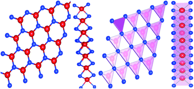 |
| | Fig. 1 Top view and side view of the 2D structure of 1H-MoS2 (Mo – red and S – blue with a polyhedral cage). | |
3 Results and discussion
3.1 Electronic properties
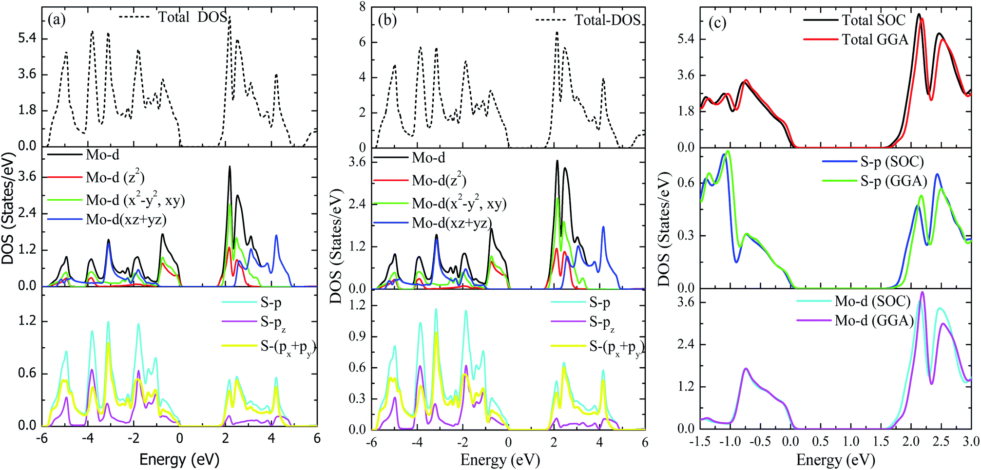
Top and side views of the 2D structure of MoS2 are presented in Fig. 1. The lattice arrangement of MoS2 shows clear bonds between the S and Mo atoms, keeping a void or hollow in the central part. Therefore, the top view exactly resembles a 2D graphene-like structure. Six S atoms and one Mo atom form two symmetrical pyramidal polyhedrons, and the Mo atom is at the junction of the two pyramids. The presence of bonding between the S and Mo atoms may be the reason for p–d hybridization which leads to metallic bonding and the absence of van der Waals interactions. The electronic properties are investigated by calculating the density of states (DOS) and band structure of MoS2 as shown in Fig. 2 and 3. Based on both (GGA and SOC) calculations, MoS2 exhibits a clear band gap at the Fermi level (EF), showing the existence of semiconducting behaviour. The maxima and minima of the dispersed bands are observed at the high symmetry K point. The probability of electron transitions along the K–K symmetry points indicates that MoS2 is a direct band gap semiconductor. The origin of the energy band gap is due to the Mo-d orbital and S-p orbital hybridization, as discussed elsewhere.14,61,64–67 For further elucidation of the band structure we have calculated the partial density of states (PDOS) as well. Fig. 2(a and b) display the partial DOS calculated with GGA and GGA–SOC, respectively. A comparison of the total and partial DOS calculated with GGA and SOC is also presented in Fig. 2(c). Fig. 2(a and b) are divided into three layers: top (total DOS), middle (partial DOS of Mo atoms) and bottom (partial DOS of S atoms). The PDOS of the S atoms represents the 3p states. The first relative magnitude of the 3p states of the S atoms in monolayer MoS2 (0.31 states per eV) is the same for both GGA and GGA+SOC calculations [Fig. 2(a and b)]. The above results obtained from Fig. 2 and 3 indicate that monolayer MoS2 is a direct band gap semiconductor with electron transitions along the K-symmetry points. The major contribution is attributed to Mo-d and S-p states. The valence band (VB) in the range from 0 to −6 eV is an admixture of both Mo-d and S-p states due to the p–d orbital hybridization [Fig. 2(a)]. Whereas, in the conduction band (CB), the energy range from 1.75 to 5 eV is mainly composed of occupied Mo-d states with a small contribution from the S-p states. From Fig. 3 (right side), we can see the significant effect of GGA+SOC on the electronic band structure with the splitting of the valence band maximum (VBM). We have observed that the completely filled Mo-dz2 state lies at the VBM (Fig. 3). Meanwhile on implementation of GGA+SOC, the occupied Mo-dz2 state is pushed towards lower energy while the Mo-dx2−y2,xy band is ∼0.026 eV higher in energy on approaching the EF [Fig. 3 (middle bottom line marked by an arrow head) and Fig. 4]. This “split-off” energy is almost half of the experimentally measured value of 0.042 eV.68 Also, the unoccupied Mo-dz2 state at the CBM drops down by a small amount of energy as compared to the GGA band, as shown in Fig. 2(b). Thus, GGA+SOC reduces the GGA band gap from ∼1.75 eV to ∼1.68 eV. The presence of two degenerate bands at the VBM along the K-symmetry point on the application of SOC is probably due to the Mo-dx2−y2,xy and Mo-dz2 states.
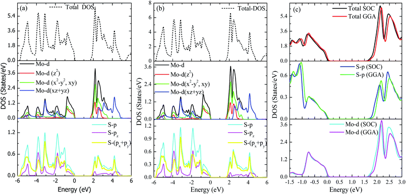 |
| | Fig. 2 Total and partial DOS of MoS2. (a) GGA, (b) GGA–SOC and (c) both GGA and GGA–SOC together. | |
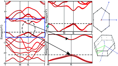 |
| | Fig. 3 Band structure of 1H-MoS2 (GGA: black lines and GGA–SOC: red lines), first Brillouin zone, and primitive cell (blue arrows indicate reciprocal lattice vectors, green lines represent the high symmetry points). | |
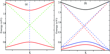 |
| | Fig. 4 Valence band maxima and conduction band minima calculated with (a) GGA and (b) GGA+SOC. | |
3.2 Thermoelectric properties
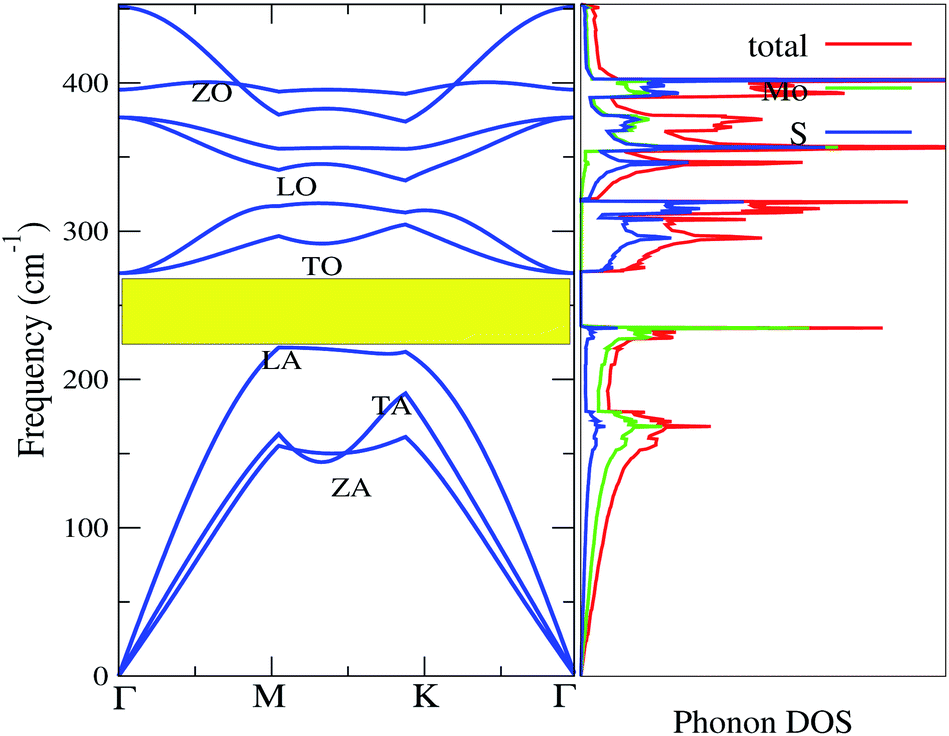
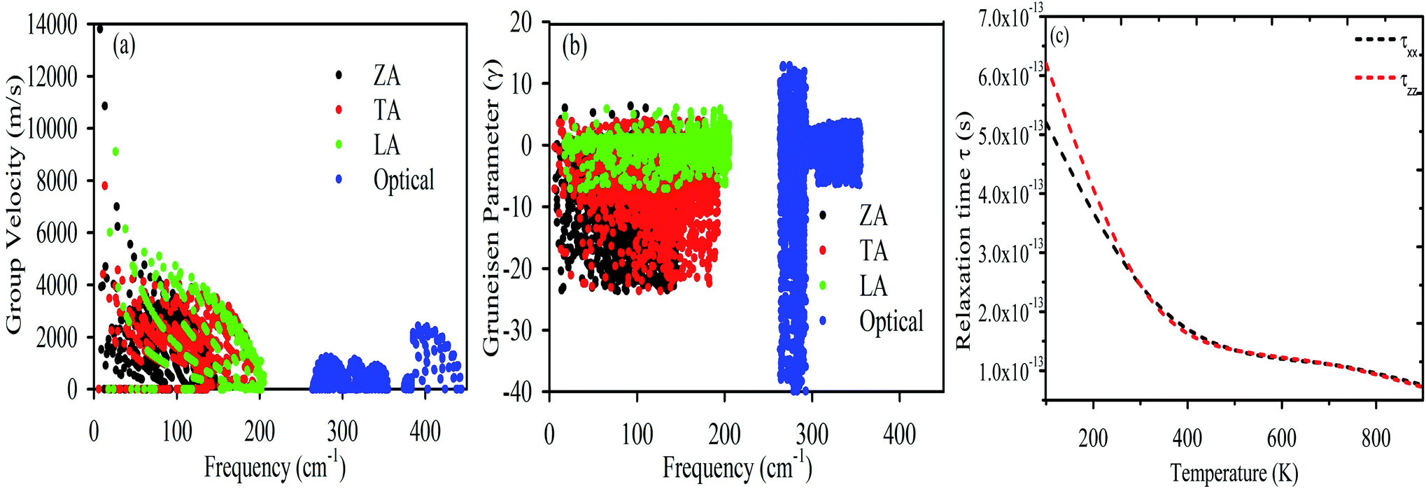
To confirm the thermodynamical stability for practical synthesis, we have calculated the frequency-dependent phonon dispersion using density functional perturbation theory (DFPT)63,69,70 as shown in Fig. 5. The presence of phonon modes in the positive frequency range indicates that monolayer MoS2 is dynamically stable for laboratory synthesis. The three atoms in the primitive cell give nine distinctive vibrational modes along the Γ-point. The nine phonon branches are mixtures of three acoustic (lower frequency) and six optical (higher frequency) branches. As shown in Fig. 5, the acoustic modes are identified as the transverse mode (TA), longitudinal mode (LA), and out-of-plane mode (ZA) whereas the optical branches are composed of two transverse modes (TO) at the bottom, two longitudinal modes (LO) in the middle and two out-of-plane modes (ZO) at the top. The optical mode (TO) and acoustic mode (LA) are well separated by ∼52 cm−1. The finite frequency band gap as a result of LA–TO splitting may be attributed to the large difference in the atomic masses (Mo = 95.96 amu and S = 32.06 amu). The optical branches along the Γ symmetry points are at ∼275 cm−1, ∼370 cm−1, ∼395 cm−1 and ∼460 cm−1, consistent with the previous results.37,62 Fig. 6 demonstrates the phonon transport related parameters: (a) group velocity at 300 K, (b) Grüneisen parameter at 300 K and (c) relaxation time (τ). The three acoustic modes have the highest group velocity and Grüneisen parameter at a particular frequency and q-point. This indicates high phonon–phonon scattering rates in which most of the heat is transported by the transverse acoustic mode (TA) and longitudinal acoustic mode (LA).71,72 Therefore, the lattice thermal conductivity can be further reduced by doping with the dissipation of heat that may be introduced by the acoustic–optical phonon scattering channels.73 The group velocity of the ZA mode can reach ∼14 km s−1 at a particular phonon frequency. However, the observation of low group velocity at higher frequencies for the optical modes indicates a small but significant contribution to the thermal conductivity. Anharmonicity results in enhanced phonon–phonon scattering, which reduces κl without affecting the electronic properties.74 The Grüneisen parameter measures the strength of the anharmonicity. Therefore, the larger the Grüneisen parameter, the stronger the phonon scattering. The high value of the Grüneisen parameter suggests high anharmonicity in 2D-MoS2 and intense phonon scattering. The short phonon relaxation time of 2D-MoS2 also indicates intense phonon scattering.
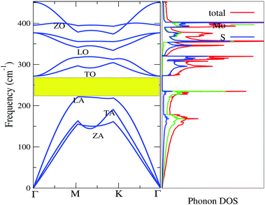 |
| | Fig. 5 Phonon bands and phonon DOS of 2D monolayer MoS2. | |
 |
| | Fig. 6 (a) Group velocity, (b) Grüneisen parameter and (c) phonon relaxation time (τp). | |
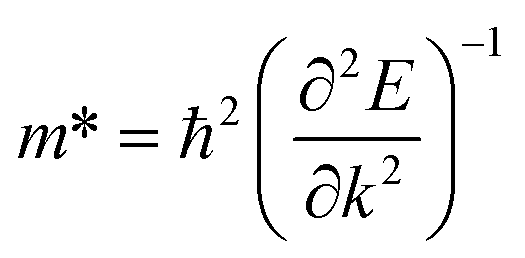
The description of electron transport in a solid-state material is directly related to the electronic energy bands which give rise to a thermoelectric response measured in terms of a dimensionless figure of merit ZT as already presented in eqn (1). As reported earlier, monolayered MoS2 is a semiconductor with a direct band gap value of ∼1.8 eV.14,64,67 In semiconductors, the effective mass (m*) plays a vital role in deriving the quantitative transport characteristics. The effective mass of a charge carrier can be obtained from the parabolic band near EF based on the energy-independent scattering approximation79,80 given by eqn (2).
| |
 | (2) |
The effect of SOC leads to splitting of the band near EF close to the VBM which results in two effective masses for holes [cf. Fig. 3 and 4]. A lower value of effective mass leads to a higher value for the charge mobility. On the other hand, the electrical conductivity (σ) is directly related to the charge carrier mobility via eqn (3)
where
n is the concentration of charge carriers and
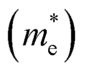
e is the electron charge. The calculated effective masses for electrons

and holes

are presented in
Table 1. Our calculated values of the effective masses are

= 0.391 (GGA),

= 0.552 (GGA),

= 0.315 (SOC) and

= 0.467 (SOC); these values are in good agreement with the earlier results estimated with the GGA,
75 DFT-HSE
78 and tight binding (TB)
78 approaches. The lattice part of the thermal conductivity
κl has been determined by using the Phono3py code
63 which iteratively solves the BTE from
eqn (4):
| |
 | (4) |
where
Ω is the primitive cell volume,
α and
β are the Cartesian components,
kB is the Boltzmann constant,
ωλ and
vλ are the angular frequency and group velocity,
τλ denotes the phonon relaxation time and
f0 is the Bose–Einstein distribution function near
EF.
Table 1 Calculated energy band gap (Eg) in eV and effective masses (m*) of electrons  and holes
  in terms of electron mass (me)
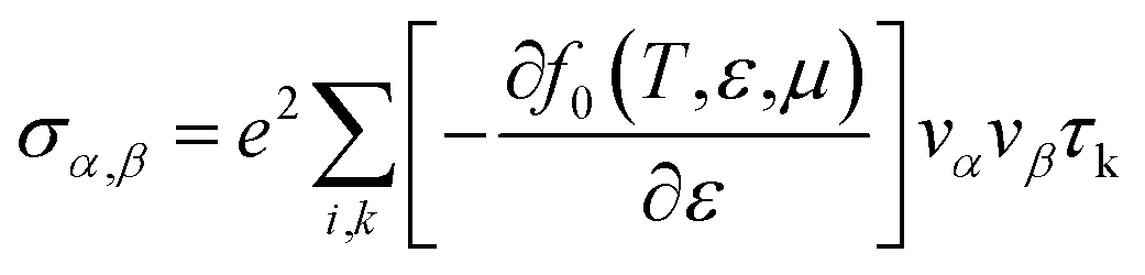
The electron parts of the thermoelectric parameters are given by eqn (5)–(9) as presented in the BoltzTraP user manual.57
Here σα,β are the electrical conductivity tensors,
| |
 | (5) |
where
α and
β refer to the tensor indices,
vα and
vβ are the group velocities,
e is the charge of the electron and
τk is the electron relaxation time. The contributions of the electrons are mostly found near the Fermi energy (
EF), termed as the chemical potential (
μ) (
μ −
kBT <
ε <
μ +
kBT) where
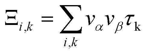
kB is the Boltzmann constant. The kernel of the transport distribution is given by:
| |
 | (6) |
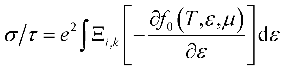
The electron relaxation time (τ) dependent electrical conductivity (σ/τ), thermal conductivity (κ/τ) and Seebeck coefficient can be written as
| |
 | (7) |
| |
 | (8) |
| |
 | (9) |
where
f0 is a Fermi–Dirac distribution function.
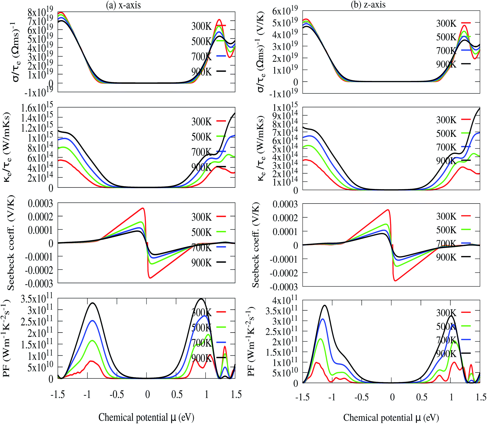
The relaxation time (τe) dependent electrical conductivity (σ), Seebeck coefficient (S), electron thermal conductivity (κe) and power factor (PF) as a function of chemical potential (eV) along the x- and z-axes are shown in Fig. 7(a and b), respectively. The electron parts of the thermoelectric parameters are strongly dependent on the electron relaxation time (τe). The thermoelectric efficiency (ZT) value cannot be estimated unless and until τe is decoupled. Therefore, we have performed the electron transport calculation by using the modified BoltzTraP code based on the electron carrier relaxation time. The expression for electron relaxation time is given by eqn (10)82,83
| |
 | (10) |
where
Ω refers to the volume of the primitive cell,
ℏ is Planck’s constant,
v is the phonon mode index,
![[small omega, Greek, macron]](https://www.rsc.org/images/entities/i_char_e0da.gif) v
v is the averaged phonon mode energy,
gv2 is the averaged electron–phonon matrix,
n(
v,
T) is the Bose–Einstein distribution function,
f(
ε +
v,
μ,
T) refers to the Fermi–Dirac distribution function,
gs = 2 is the spin degeneracy,
ε is the electron energy, and
ρ is the density of states per unit energy and unit volume (
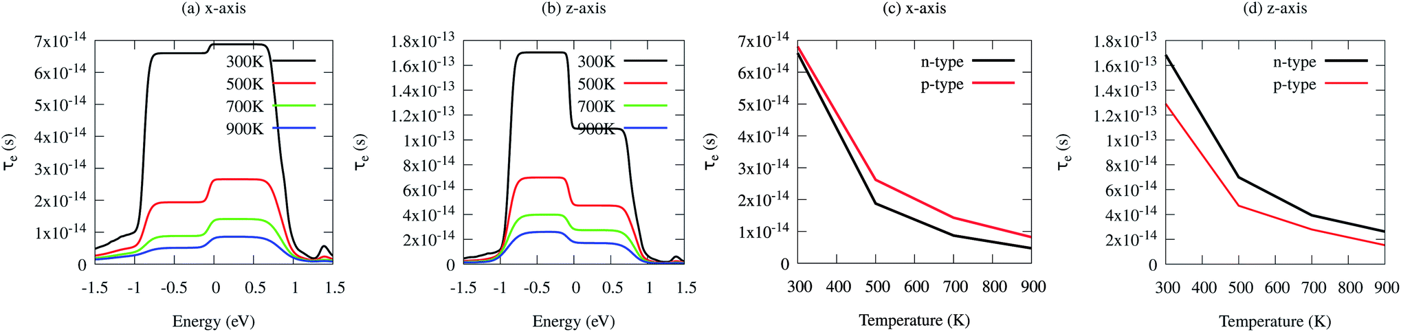
V). The electron relaxation times along both the
x- and
z-axes as a function of chemical potential and absolute temperature are presented in
Fig. 8(a–d). The electron relaxation times along the
z-axis are longer than those along the
x-axis for both n-type and p-type carriers. However, the electron relaxation times of n-type and p-type carriers along the same axis are almost the same. The electrons in the conduction band which lies close to the Fermi energy shows longer relaxation times as compared to the holes in the valence bands along the
x-axis. This is in contrast to the carriers along the
z-axis. For both carriers,
τe decreases with an increase in absolute temperature. The sharp decrease in
τe near the band edges can be visualised as
eqn (11)82
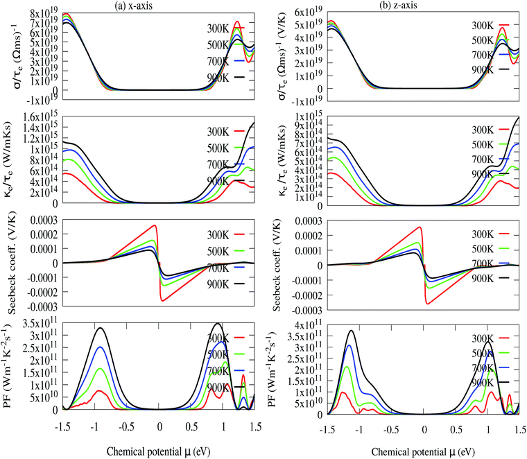 |
| | Fig. 7 (a) In-plane x-axis: electron relaxation time (τe) dependent electrical conductivity (σ/τe), electron thermal conductivity (κe/τe), Seebeck coefficient (S) and power factor (PF), (b) out-of-plane z-axis: electron relaxation time (τe) dependent electrical conductivity (σ/τe), electron thermal conductivity (κe/τe), Seebeck coefficient (S) and power factor (PF). | |
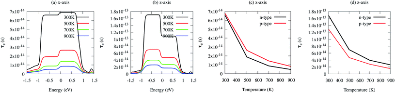 |
| | Fig. 8 (a) Electron relaxation time (τe) as a function of chemical potential along the x-axis, (b) electron relaxation time (τe) as a function of chemical potential along the z-axis, (c) electron relaxation time (τe) as a function of temperature along the x-axis and (d) electron relaxation time (τe) as a function of temperature along the z-axis. | |
Eqn (11) established an inverse relation between τe and the carrier density of states per unit energy and volume (ρ), while the electron–phonon matrix elements (g) depend weakly on the energy. The τe value increases from ∼1 × 10⁻¹⁴ s to ∼7 × 10⁻¹⁴ s along the x-axis and from ∼2.0 × 10⁻¹⁴ s to ∼1.8 × 10⁻¹³ s along the z-axis as the temperature decreases from 900 K to 300 K [see Fig. 8(a–d)].
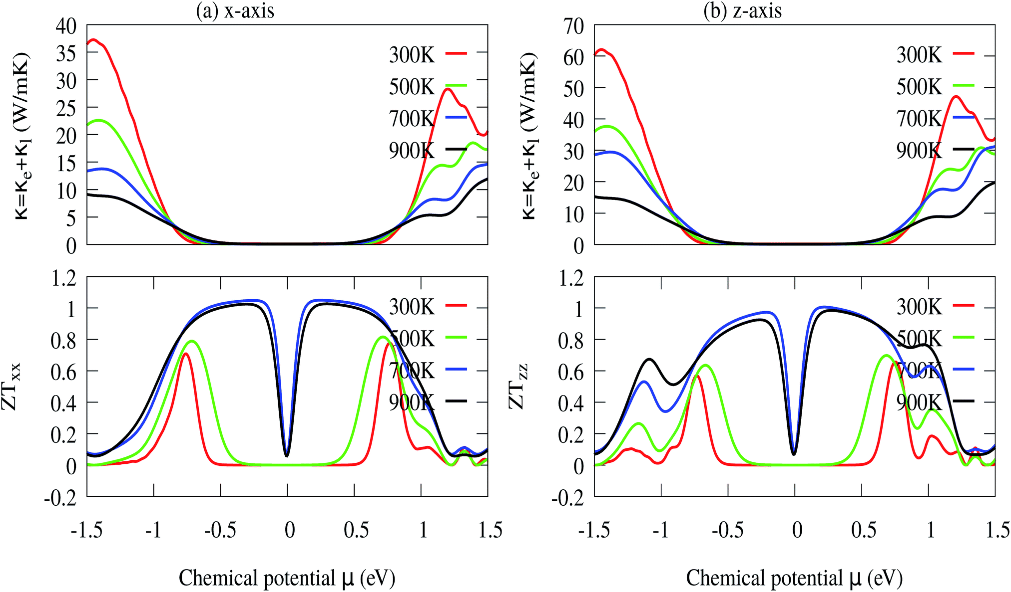
The optimized values of the thermoelectric parameters obtained at 300 K are presented in Table 2. The high value of S and low κl are indicative that the monolayer MoS2 system can be a prospective candidature for thermoelectric applications. However, the presence of a wide band gap in monolayer MoS2 may result in a low value of electrical conductivity (σ). The use of SOC has a significant effect on the band energy of MoS2 due to the sizeable spatial expansion of the Mo-3d-orbital which may lead to desirable physical and chemical properties. The spin–orbit interaction is applied along the easy spin quantization axis [001] direction. We found that the large GGA band gap of the monolayer MoS2 semiconductor was reduced to ∼1.68 eV which may enhance the power factor. Hence, we have calculated all the thermoelectric properties using GGA–SOC. The calculated σ for both n-type and p-type carriers along the x-axis are found to decrease from ∼5.0 × 10⁵ to ∼5 × 10⁴ Ω−1 m−1 with an increase in absolute temperature from 300 to 900 K. Similarly, along the z-axis, σ varies from ∼1.45 × 10⁶ to ∼1.5 × 10⁵ Ω−1 m−1 in the same temperature range. At room temperature the total thermal conductivities are found to be κxx = ∼36.23 W m−1 K−1 and κxx = ∼30.18 W m−1 K−1 for n-type and p-type carriers, respectively. On the other hand, the calculated room temperature values of the total thermal conductivities along the z-axis are almost two times higher, κzz = ∼60.00 W m−1 K−1 and κzz = ∼50.84 W m−1 K−1 for n-type and p-type carriers, respectively. Our results for total thermal conductivity measured along the x-axis are consistent with the results obtained from molecular dynamics (23.2 W m−1 K−1) and from a non-equilibrium Green’s function (26.2 W m−1 K−1).52 Moreover, the results along the z-axis agree well with the values of 52 W m−1 K−1 (ref. 35) and 85–110 W m−1 K−1 (ref. 54) measured for the vapour phase of few-layer MoS2 and the (001) orientation of a MoS2 crystal with basal plane thermal conductivity as a function of laser spot size, respectively. We observed a sharp decrease in κ as the temperature increased from 300 K to 900 K [Fig. 9(a and b)]. A similar trend has also been reported for WS2, in which κl decreases from 150 to 100 W m−1 K−1within the 200–500 K temperature range. Also, in WSe2, κl decreases from 50 to 30 W m−1 K−1 in the same temperature range.81 The sharp rise in DOS near the Fermi energy gives rise to the high value of S. The maximum values of S are found to be ∼1.19 × 10⁻⁴ V K−1 and ∼1.41 × 10⁻⁴ V K−1 for the n-type and the p-type carriers along the x-axis, respectively. Fig. 9(a and b) display the total thermal conductivity (κ = κl + κe) and figure of merit (ZT) as a function of chemical potential along the x- and z-axes, respectively. For both the x- and z-axes, the ZT value due to hole carriers (p-type) surpasses the n-type ZT value. The ZT values are found to be 0.60–0.76 at room temperature which seems to be too small for practical applications [Table 2]. Interestingly, the ZT increases up to ∼1.00 at 1000 K for p-type carriers (taken from the peak value) [see Fig. 9(a and b)]. The linear behaviour of ZT as a function of temperature signifies the potential of monolayer MoS2 as a high temperature thermoelectric material.
Table 2 Calculated σ (Ω−1 m−1), S (V K−1), τe (s), κ = κe + κl (W m−1 K−1) and thermoelectric efficiency (ZT) at 300 K (all calculations are performed with GGA–SOC)
| Carriers |
σ |
S |
τe |
κ = κe + κl |
ZT |
| Along xx |
| n-type |
5.13 × 10⁵ |
−0.119 × 10⁻³ |
6.807 × 10⁻¹⁴ |
36.238 |
0.75 |
| p-type |
3.26 × 10⁵ |
0.141 × 10⁻³ |
6.602 × 10⁻¹⁴ |
30.180 |
0.76 |
![[thin space (1/6-em)]](https://www.rsc.org/images/entities/char_2009.gif) |
| Along zz |
| n-type |
6.192 × 10⁵ |
−1.12 × 10⁻⁴ |
1.648 × 10⁻¹³ |
60.00 |
0.60 |
| p-type |
14.07 × 10⁵ |
1.25 × 10⁻⁴ |
1.291 × 10⁻¹³ |
50.84 |
0.62 |
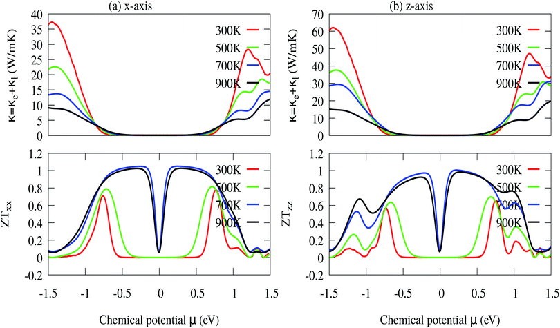 |
| | Fig. 9 (a) In-plane x-axis: total thermal conductivity (κ = κe + κl) and ZTxx, and (b) out-of-plane z-axis: total thermal conductivity (κ = κe + κl) and ZTzz. | |
4 Conclusion
In this investigation, we have studied the electronic and thermoelectric properties of monolayer MoS2 using the GGA and GGA–SOC approaches. The calculation of the electronic structure shows that monolayer MoS2 is a direct band gap semiconductor, as the CBM and VBM lie at the same K-symmetry point. The calculated band gap is found to be 1.75 eV, in good agreement with the previous experimental and theoretical results. Monolayer MoS2 exhibits high S and low κ values, which are crucial for thermoelectric applications. However, with GGA the electrical conductivity (σ) is observed to be suppressed which eventually limits the thermoelectric power factor due to the presence of a wide band gap. We have found that SOC has a significant effect on the band energy of monolayer MoS2 due to the presence of the larger 4d orbital. A reduction of the direct band gap has been observed on application of spin–orbit coupling along the spin quantization 001 direction. The reduced band gap is expected to enhance σ at room temperature. Our calculated thermoelectric parameters are consistent with the available data. The reduced lattice thermal conductivity at elevated temperatures is another interesting feature. As a result, the ZT value approaches the benchmark value of ∼1.0 at a temperature of ∼1000 K.
Conflicts of interest
All authors declare that there are no conflicts of interest.
Acknowledgements
D. P. Rai acknowledges a Core Research Grant from the Department of Science and Technology SERB (CRG DST-SERB, Govt. of India, New Delhi) via Sanction no. CRG/2018/000009(Ver-1). A. Laref acknowledge the Research Center of Female Scientific and Medical College, King Saud University for financial support. Sohail Ahmad would like to express gratitude to King Khalid University, Abha, Saudi Arabia for administrative and technical support. Tuan V. Vu acknowledges the Vietnam National Foundation for Science and Technology Development (NAFOSTED) under grant number 103.01-2018.334.
Notes and references
- F. Schwierz, Graphene Transistors: Status, Prospects, and Problems, Proc. IEEE, 2013, 101, 1567–1584 CAS.
- X. Huang, Z. Y. Yin, S. X. Wu, X. Y. Qi, Q. Y. He, Q. C. Zhang, Q. Y. Yan, F. Boey and H. Zhang, Graphene-based materials: synthesis, characterization, properties, and applications, Small, 2011, 7, 1876–1902 CrossRef CAS PubMed.
- D. P. Rai, S. Kaur and S. Srivastava, Band gap modulation of mono and bi-layer hexagonal ZnS under transverse electric field and bi-axial strain: a first principles study, Phys. B, 2018, 531, 90–94 CrossRef CAS.
- Y. Kim, J. L. Huang and C. M. Lieber, Characterization of nanometer scale wear and oxidation of transition metal dichalcogenide lubricants by atomic force microscopy, Appl. Phys. Lett., 1991, 59, 3404–3406 CrossRef CAS.
- K. H. Hu, X. G. Huand and X. J. Sun, Morphological effect of MoS2 nanoparticles on catalytic oxidation and vacuum lubrication, Appl. Surf. Sci., 2010, 256, 2517–2523 CrossRef CAS.
- E. Fortin and W. Sears, Photovoltaic effect and optical absorption in MoS2, J. Phys. Chem. Solids, 1982, 43, 881–884 CrossRef CAS.
- A. H. Reshak and S. Auluck, Calculated optical properties of 2H-MoS2 intercalated with lithium, Phys. Rev. B: Condens. Matter Mater. Phys., 2003, 68, 125101–125107 CrossRef.
- K. K. Liu, W. Zhang, Y. H. Lee, Y. C. Lin, M. T. Chang, C. Y. Su, C. S. Chang, H. Li, Y. Shi and H. Zhang, Growth of Large-Area and Highly Crystalline MoS2 Thin Layers on Insulating Substrates, Nano Lett., 2012, 12, 1538–1544 CrossRef CAS PubMed.
- Y. H. Lee, X. Q. Zhang, W. Zhang, M. T. Chang, C. T. Lin, K. D. Chang, Y. C. Yu, J. T. W. Wang, C. S. Chang, L. J. Li and T. W. Lin, Synthesis of large-area MoS2 atomic layers with chemical vapor deposition, Adv. Mater., 2012, 24, 2320–2325 CrossRef CAS PubMed.
- R. J. Smith, P. J. King, M. Lotya, C. Wirtz, U. Khan, S. De, A. O’Neill, G. S. Duesberg, J. C. Grunlan and G. Moriarty, Large Scale Exfoliation of Inorganic Layered Compounds in Aqueous Surfactant Solutions, Adv. Mater., 2011, 23, 3944–3948 CrossRef CAS PubMed.
- C. Lee, H. Yan, L. E. Brus, T. F. Heinz, J. Hone and S. Ryu, Anomalous Lattice Vibrations of Single- and Few-Layer MoS2, ACS Nano, 2010, 4, 2695–2700 CrossRef CAS PubMed.
- B. Radisavljevic, A. Radenovic, J. Brivio, V. Giacometti and A. Kis, Single-layer MoS2 transistors, Nat. Nanotechnol., 2011, 6, 147–150 CrossRef CAS PubMed.
- R. Yan, J. R. Simpson, S. Bertolazzi, J. Brivio, M. Watson, X. Wu, A. Kis, T. Luo, A. R. H. Walker and H. G. Xing, Thermal Conductivity of Monolayer Molybdenum Disulfide Obtained from Temperature-Dependent Raman Spectroscopy, ACS Nano, 2014, 8, 986–993 CrossRef CAS PubMed.
- K. F. Mak, C. Lee, J. Hone, J. Shan and T. F. Heinz, Atomically Thin MoS2: A New Direct-Gap Semiconductor, Phys. Rev. Lett., 2010, 105, 136805 CrossRef PubMed.
- D. P. Rai, V. V. Tuan, A. Laref, M. P. Ghimire, P. K. Patra and S. Srivastava, Electronic and optical properties of 2D monolayer (ML) MoS2 with vacancy defect at S sites, Nano-Struct. Nano-Objects, 2020, 21, 100404, DOI:10.1016/j.nanoso.2019.100404.
- F. J. Urbanos, A. Black, R. B. Gavito, A. L. Vázquez de Parga, R. Miranda and D. Granados, Electrical and geometrical tuning of MoS2 field effect transistors via direct nanopatterning, Nanoscale, 2019, 11, 11152–11158 RSC.
- T. Pham, G. Li, E. Bekyarova, M. E. Itkis and A. Mulchandani, MoS2-based optoelectronic gas sensor with sub-parts-per-billion limit of NO2 gas detection, ACS Nano, 2019, 13, 3196–3205 CrossRef CAS PubMed.
- N. Goel, R. Kumar and M. Kumar, Enhanced sensing response with complete recovery of MoS2 sensor under photoexcitation, AIP Conf. Proc., 2018, 1942, 050060–050064 CrossRef.
- L. Zhe, M. Nasir, T. Muhammad, P. Lun, Z. Xiangwen and Z. Ji-Jun, Fabrication of zero to three dimensional nanostructured molybdenum sulfides and their electrochemical and photocatalytic applications, Nanoscale, 2016, 8, 18250–18269 RSC.
- P. Zhao, A. Khosravi, A. Azcatl, P. Bolshakov, G. Mirabelli, E. Caruso, C. L. Hinkle, P. K. Hurley, R. M. Wallace and C. D. Young, Evaluation of border traps and interface traps in HfO2/MoS2 gate stacks by capacitance-voltage analysis, 2D Mater., 2018, 5, 031002–031008 CrossRef.
- X. He, H. Li, Z. Zhu, Z. Dai, Y. Yang, P. Yang, Q. Zhang, P. Li, U. Schwingenschlogl and X. Zhang, Strain engineering in monolayer WS2, MoS2, and the WS2/MoS2 heterostructure, Appl. Phys. Lett., 2016, 109, 173105 CrossRef.
- H. V. Phuc, N. N. Hieu, B. D. Hoi, N. V. Hieu, T. V. Thu, N. M. Hung, V. V. Ilyasov, N. A. Poklonski and C. V. Nguyen, Tuning the Electronic Properties, Effective Mass and Carrier Mobility of MoS2 Monolayer by Strain Engineering: First-Principle Calculations, J. Electron. Mater., 2018, 47, 730–736 CrossRef CAS.
- A. Kumar and P. Ahluwalia, A first principle comparative study of electronic and optical properties of 1H-MoS2 and 2H-MoS2, Mater. Chem. Phys., 2012, 135, 755–761 CrossRef CAS.
- K. P. Dhakal, D. L. Duong, J. Lee, H. Nam, M. Kim, M. Kan, Y. H. Lee and J. Kim, Confocal absorption spectral imaging of MoS2: optical transitions depending on the atomic thickness of intrinsic and chemically doped MoS2, Nanoscale, 2014, 6, 13028–13035 RSC.
- N. N. Hieu, V. V. Ilyasov, T. V. Vu, N. A. Poklonski, H. V. Phuc, L. T. T. Phuong, B. D. Hoi and C. V. Nguyen, First principles study of optical properties of molybdenum disulfide: from bulk to monolayer, Superlattices Microstruct., 2018, 115, 10–18 CrossRef CAS.
- Q. H. Wang, K. K. Zadeh, A. Kis, J. N. Coleman and M. S. Strano, Electronics and optoelectronics of two-dimensional transition metal dichalcogenides, Nat. Nanotechnol., 2012, 7, 699–712 CrossRef CAS PubMed.
- S. Sharma, S. Kumar and U. Schwingenschlögl, Arsenene and Antimonene: Two-Dimensional Materials with High Thermoelectric Figures of Merit, Phys. Rev. Appl., 2017, 8, 044013–044018 CrossRef.
- M. Tahir and U. Schwingenschlögl, Tunable thermoelectricity in monolayers of MoS2 and other group-VI dichalcogenides, New J. Phys., 2014, 16, 115003–115011 CrossRef.
- G. H. Hong, Y. Teng, T. Peng and Z. Z. Dong, Theoretical study of thermoelectric properties of MoS2, Chin. Phys. B, 2014, 23, 017201–017207 CrossRef.
- D. P. Rai, A. Shankar, Sandeep, M. P. Ghimire, R. Khenata and R. K. Thapa, Study of the enhanced electronic and thermoelectric (TE) properties of ZrxHf1−x−yTayNiSn: a first principles study, RSC Adv., 2015, 5, 95353–95359 RSC.
- K. Kaur, R. Kumar and D. P. Rai, A promising thermoelectric response
of HfRhSb half Heusler compound at high temperature: a first principle study, J. Alloys Compd., 2018, 763, 1018–1023 CrossRef CAS.
- K. Kaur, D. P. Rai, R. K. Thapa and S. Srivastava, Structural, electronic, mechanical, and thermoelectric properties of a novel half Heusler compound HfPtPb, J. Appl. Phys., 2017, 122, 045110–045117 CrossRef.
- D. P. Rai, Sandeep, A. Shankar, R. Khenata, A. H. Reshak, C. E. Ekuma, R. K. Thapa and S.-H. Ke, Electronic, optical, and thermoelectric properties of Fe2+xV1−xAl, AIP Adv., 2017, 7, 045118 CrossRef.
- D. Wickramaratne, F. Zahid and R. K. Lake, Electronic and thermoelectric properties of few-layer transition metal dichalcogenides, J. Chem. Phys., 2014, 140, 124710–124713 CrossRef PubMed.
- S. Sahoo, A. P. S. Gaur, M. Ahmadi, M. J. F. Guinel and R. S. Katiyar, Temperature-Dependent Raman Studies and Thermal Conductivity of Few-Layer MoS2, J. Phys. Chem. C, 2013, 117, 9042–9047 CrossRef CAS.
- X. Wei, Y. Wang, Y. Shen, G. Xie, H. Xiao, J. Zhong and G. Zhang, Phonon thermal conductivity of monolayer MoS2: a comparison with single layer graphene, Appl. Phys. Lett., 2014, 105, 103902–103905 CrossRef.
- G. Zhang and Y. W. Zhang, Thermoelectric properties of two-dimensional transition metal dichalcogenides, J. Mater. Chem. C, 2017, 5, 7684–7698 RSC.
- D. Qin, P. Yan, G. Ding, X. Ge and G. Gao, Monolayer PdSe2: a promising two-dimensional thermoelectric material, Sci. Rep., 2018, 8, 2764–2768 CrossRef PubMed.
- K. Hippalgaonkar, Y. Wang, Y. Ye, H. Zhu, Y. Wang, J. Moore and X. Zhang, High thermoelectric power factor in two-dimensional crystals of MoS2, Phys. Rev. B, 2017, 95, 115407–115409 CrossRef.
- Z. Jin, Q. Liao, H. Fang, Z. Liu, W. Liu, Z. Ding, T. Luo and N. Yang, A Revisit to High Thermoelectric Performance of Single-layer MoS2, Sci. Rep., 2015, 5, 18342–18347 CrossRef CAS PubMed.
- W. Huang, H. Da and G. Liang, Thermoelectric performance of MX2 (M = Mo, W; X = S, Se) monolayers, J. Appl. Phys., 2013, 113, 104304–104307 CrossRef.
- S. Kumar and U. Schwingenschlögl, Thermoelectric Response of Bulk and Monolayer MoSe2 and WSe2, Chem. Mater., 2015, 27, 1278–1284 CrossRef CAS.
- A. N. Gandi and U. Schwingenschlögl, WS2 As an Excellent High-Temperature Thermoelectric Material, Chem. Mater., 2014, 26, 6628–6637 CrossRef CAS.
- Y. Su, M. A. Ebrish, E. J. Olson and S. J. Koester, SnSe2 field-effect transistors with high drive current, Appl. Phys. Lett., 2013, 103, 263104 CrossRef.
- A. Arab, A. V. Davydov, D. A. Papaconstantopoulos and Q. Li, Monolayer MoS2 Nanoribbons as a Promising Material for Both n-type and p-type Legs in Thermoelectric Generators, J. Electron. Mater., 2016, 45, 5253–5263 CrossRef CAS.
- H. Lv, W. Lu, D. Shao, H. Lu and Y. Sun, Strain-induced enhancement in the thermoelectric performance of a ZrS2 monolayer, J. Mater. Chem. C, 2016, 4, 4538–4545 RSC.
- G. Ding, G. Y. Gao, Z. Huang, W. Zhang and K. Yao, Thermoelectric properties of monolayer MSe2 (M = Zr, Hf): low lattice thermal conductivity and a promising figure of merit, Nanotechnology, 2016, 27, 375703–375707 CrossRef PubMed.
- C. Chiritescu, D. G. Cahill, N. Nguyen, D. Johnson, A. Bodapati, P. Keblinski and P. Zchack, Ultralow Thermal Conductivity in Disordered, Layered WSe2 Crystals, Science, 2007, 315, 351–353 CrossRef CAS PubMed.
- V. Varshney, S. S. Patnaik, C. Muratore, A. K. Roy, A. A. Voevodin and B. L. Farmer, MD simulations of molybdenum disulphide (MoS2): force-field parameterization and thermal transport behavior, Comput. Mater. Sci., 2010, 48, 101–108 CrossRef CAS.
- J. W. Jiang, H. S. Park and T. Rabczuk, Molecular dynamics simulations of single-layer molybdenum disulphide (MoS2): Stillinger-Weber parametrization, mechanical properties, and thermal conductivity, J. Appl. Phys., 2013, 114, 064307–064310 CrossRef.
- X. J. Liu, G. Zhang, Q. X. Pei and Y. W. Zhang, Phonon thermal conductivity of monolayer MoS2 sheet and nanoribbons, Appl. Phys. Lett., 2013, 103, 133113–133115 CrossRef.
- Y. Cai, J. Lan, G. Zhang and Y. W. Zhang, Lattice vibrational modes and phonon thermal conductivity of monolayer MoS2, Phys. Rev. B: Condens. Matter Mater. Phys., 2014, 89, 035438 CrossRef.
- W. Li, J. Carrete and N. Mingo, Thermal conductivity and phonon linewidths of monolayer MoS2 from first principles, Appl. Phys. Lett., 2013, 103, 253103–253104 CrossRef.
- J. Liu, G. M. Choi and D. G. Cahill, Measurement of the anisotropic thermal conductivity of molybdenum disulfide by the time-resolved magneto-optic Kerr effect, J. Appl. Phys., 2014, 116, 233107 CrossRef.
- K. Kaur, D. Murali and B. R. K. Nanda, Stretchable and dynamically stable promising two-dimensional thermoelectric materials: ScP and ScAs, J. Mater. Chem. A, 2019, 7, 12604–12615 RSC.
- M. Buscema, M. Barkelid, V. Zwiller, H. S. van der Zant and G. A. Steele, Large and Tunable Photothermoelectric Effect in Single-Layer MoS2, Nano Lett., 2013, 13, 358–363 CrossRef CAS PubMed.
- G. K. H. Madsen and D. J. Singh, BoltzTraP. A code for calculating band-structure dependent quantities, Comput. Phys. Commun., 2006, 175, 67–71 CrossRef CAS.
- P. Blaha, K. Schwarz, G. K. H. Madsen, D. Kvasnicka, J. Luitz and K. Schwarz, An Augmented Plane Wave plus Local Orbitals Program for Calculating Crystal Properties. Wien2K User’s Guide, Techn. Universitat Austria, Wien, 2008 Search PubMed.
- P. Giannozzi, et al., QUANTUM ESPRESSO: a modular and open-source software project for quantum simulations of materials, J. Phys.: Condens. Matter, 2009, 21, 395502–395519 CrossRef PubMed.
- J. P. Perdew, K. Burke and M. Ernzerhof, Generalized Gradient Approximation Made Simple, Phys. Rev. Lett., 1996, 77, 3865–3868 CrossRef CAS PubMed.
- S. Ahmad and S. Mukherjee, A Comparative Study of Electronic Properties of Bulk MoS2 and Its Monolayer Using DFT Technique: Application of Mechanical Strain on MoS2 Monolayer, Graphene, 2014, 3, 52–59 CrossRef.
- C. E. Ekuma, S. Najmaei and M. Dubey, Electronic and vibrational properties of van der Waals heterostructures of vertically stacked few-layer atomically thin MoS2 and BP, Mater. Today Commun., 2019, 19, 383–392 CrossRef CAS.
- A. Togo, L. Chaput and I. Tanaka, Distributions of phonon lifetimes in Brillouin zones, Phys. Rev. B: Condens. Matter Mater. Phys., 2015, 91, 094306–094331 CrossRef.
- P. Johari and V. B. Shenoy, Tuning the Electronic Properties of Semiconducting Transition Metal Dichalcogenides by Applying Mechanical Strains, ACS Nano, 2012, 6, 5449–5456 CrossRef CAS PubMed.
- Y. Ding, Y. Wang, J. Ni, L. R. Shi, S. Shi and W. Tang, First principles study of structural, vibrational and electronic properties of graphene-like MX2 (M = Mo, Nb, W, Ta; X = S, Se, Te) monolayers, Phys. B, 2011, 406, 2254–2260 CrossRef CAS.
- A. Splendiani, et al., Emerging photoluminescence in monolayer MoS2, Nano Lett., 2010, 10, 1271–1275 CrossRef CAS PubMed.
- A. Kuc, N. Zibouche and T. Heine, Influence of quantum confinement on the electronic structure of the transition metal sulfide TS2, Phys. Rev. B: Condens. Matter Mater. Phys., 2011, 83, 245213–245214 CrossRef.
- Y. U. Zhiyi, Y. X. Huang and S. C. Shen, Spin-orbit splitting of the valence bands in silicon determined by means of high-resolution photoconductive spectroscopy, Phys. Rev. B: Condens. Matter Mater. Phys., 1989, 39, 6287 CrossRef PubMed.
- L. Chaput, A. Togo, I. Tanaka and G. Hug, Phonon–phonon interactions in transition metals, Phys. Rev. B: Condens. Matter Mater. Phys., 2011, 84, 094302–094306 CrossRef.
- X. Gonze and C. Lee, Dynamical matrices, Born effective charges, dielectric permittivity tensors, and interatomic force constants from density-functional perturbation theory, Phys. Rev. B: Solid State, 1997, 55, 10355–10368 CrossRef CAS.
- S. Sharma, N. Singh and U. Schwingenschlögl, Two-Dimensional Tellurene as Excellent Thermoelectric Material, ACS Appl. Energy Mater., 2018, 1, 1950–1954 CrossRef CAS.
- Y. Wang, Z. Lu and X. Ruan, First principles calculation of lattice thermal conductivity of metals considering phonon–phonon and phonon–electron scattering, J. Appl. Phys., 2016, 119, 225109–225110 CrossRef.
- K. Park, A. Mohamed, M. Dutta, M. A. Stroscio and C. Bayram, Electron Scattering via Interface Optical Phonons with High Group Velocity in Wurtzite GaN-based Quantum Well Heterostructure, Sci. Rep., 2018, 8, 15947 CrossRef PubMed.
- S. Mukhopadhyay, L. Lindsay and D. J. Singh, Optic phonons and anisotropic thermal conductivity in hexagonal Ge2Sb2Te5, Sci. Rep., 2016, 6, 37076–37078 CrossRef CAS PubMed.
- W. J. Liu, M. L. Liu, B. Liu, R. G. Quhe, M. Lei, S. B. Fang, H. Teng and Z. Y. Wei, Nonlinear optical properties of MoS2–WS2 heterostructure in fiber lasers, Opt. Express, 2019, 27, 6689–6699 CrossRef CAS PubMed.
- A. Kormányos, V. Zólyomi, N. D. Drummond and G. Burkard, Spin–Orbit Coupling, Quantum Dots, and Qubits in Monolayer Transition Metal Dichalcogenides, Phys. Rev. X, 2014, 4, 011034 Search PubMed.
- J. Xi, T. Zhao, D. Wang and Z. Shuai, Tunable Electronic Properties of Two-Dimensional Transition Metal Dichalcogenide Alloys: A First-Principles Prediction, J. Phys. Chem. Lett., 2014, 5, 285–291 CrossRef CAS PubMed.
- F. Zahid, L. Liu, Y. Zhu, J. Wang and H. Guo, A generic tight-binding model for monolayer, bilayer and bulk MoS2, AIP Adv., 2013, 3, 052111–052116 CrossRef.
- G. J. Snyder and E. S. Toberer, Complex thermoelectric materials, Nat. Mater., 2008, 7, 105–114 CrossRef CAS PubMed.
- M. Cutler, J. F. Leavy and R. L. Fitzpatrick, Electronic Transport in Semimetallic Cerium Sulfide, Phys. Rev., 1964, 133, A1143–A1152 CrossRef.
- A. Mobaraki, A. Kandemir, H. Yapicioglu, O. GÃijlseren and C. Sevik, Validation of inter-atomic potential for WS2 and WSe2 crystals through assessment of thermal transport properties, Comput. Mater. Sci., 2018, 144, 92–98 CrossRef CAS.
- G. Samsonidze and B. Kozinsky, Thermoelectric Materials: Accelerated Screening of Thermoelectric Materials by First-Principles Computations of Electron–Phonon Scattering, Adv. Energy Mater., 2018, 8(20), 1800246 CrossRef.
- S. Bang, J. Kim, D. Wee, G. Samsonidze and B. Kozinsky, Estimation of electron–phonon coupling via moving least squares averaging: a method for fast-screening potential thermoelectric materials, Materials Today Physics, 2018, 6, 22–30 CrossRef.
|
| This journal is © The Royal Society of Chemistry 2020 |
Click here to see how this site uses Cookies. View our privacy policy here. 
 Open Access Article
 This Open Access Article is licensed under a
  a,
Tuan V. Vu
a,
Tuan V. Vu


 and holes
 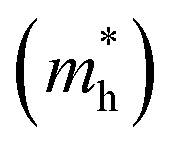 are presented in Table 1. Our calculated values of the effective masses are
  = 0.391 (GGA),
  = 0.552 (GGA),
  = 0.315 (SOC) and
  = 0.467 (SOC); these values are in good agreement with the earlier results estimated with the GGA,75 DFT-HSE78 and tight binding (TB)78 approaches. The lattice part of the thermal conductivity κl has been determined by using the Phono3py code63 which iteratively solves the BTE from eqn (4):
 and holes
  in terms of electron mass (me)