
 Open Access Article
 This Open Access Article is licensed under a Creative Commons Attribution-Non Commercial 3.0 Unported Licence
Thickness effect on VOC sensing properties of sprayed In2S3 films
R. Souissiab,
N. Bouguila *c,
B. Bourichab,
C. Vázquez-Vázquezd,
M. Bendahane and
A. Labidibf
*c,
B. Bourichab,
C. Vázquez-Vázquezd,
M. Bendahane and
A. Labidibf
aTunis University, Ecole Nationale Supérieure d'ingénieurs de Tunis (ENSIT), Tunisia
bCarthage University, Laboratoire des Matériaux, Molécules et Applications IPEST, BP 51, La Marsa 2070, Tunis, Tunisia
cGabès University, Laboratoire de Physique des Matériaux et des Nanomatériaux appliqué à l'environnement, Faculté des Sciences de Gabès, Cité Erriadh, Zrig, 6072 Gabès, Tunisia. E-mail: bouguila.nour@gmail.com
dLaboratory of Magnetism and Nanotechnology (NANOMAG), Department of Physical Chemistry, Faculty of Chemistry, Universidade de Santiago de Compostela, 15782 Santiago de Compostela, Spain
eAix Marseille Univ, Université de Toulon, CNRS, IM2NP, Marseille, France
fDepartment of Physics, College of Science and Arts at Ar-Rass, Qassim University, P.O. Box 1162, Buraydah 52571, Saudi Arabia
First published on 18th May 2020
Abstract
This work reports the thickness effect on the sensing performances of In2S3 material for some Volatile Organic Compounds (VOCs). In2S3 films were deposited on glass substrates by the spray pyrolysis technique. Different samples were prepared via changing the spray time in the range of 10–90 min. The film thickness varies from 0.8 μm to 6.1 μm. The X-ray diffraction results demonstrate that the In2S3 films are polycrystalline in nature and exhibit a cubic structure. Additionally, Scanning Electron Microscopy (SEM) and 3D profilometry examinations show that the surface roughness increases with the rising spray time. On the other hand, the oxygen adsorption versus working temperature was investigated. Sensing measurements with ethanol, methanol and acetone gases were carried out by a dynamic control of the current passing through the sensitive layers. The best sensitivity was obtained for the film matching a 70 min deposit time. An understanding of the detection mechanism based on the oxidation reaction between reduced vapors and chemisorbed oxygen was confirmed. The selectivity of the sensor was analyzed for several volatile organic compounds (VOCs).
1. Introduction
Volatile organic compounds sensors are used in a wide range of applications such as in human breath analyzers1, and food and fruit ripening monitoring devices. Many studies have recently been devoted to the development of selective and organic vapor sensitive sensors. Among the sensors developed nowadays, we can cite metal oxides including single oxide or multi-oxide structures such as LaFeO3,2 ZnCo2O4,3 CuFe2O4/Fe2O3,4 ZnO,5–7 SnO2 decorated SiO2.8 The literature review for the latest achievements has shown some very promising results. Recently, metal sulfides have been studied as a new sensitive class for vapor detection. It has been shown that cadmium sulfide (CdS) films are more sensitive to ethanol than Cadmium Oxide (CdO).9 Nevertheless, these materials are considered toxic. It is therefore important to develop non-toxic films such as Indium Sulfide In2S3. Various techniques such as spray pyrolysis,10,11 hydrothermal,12 ultrasonic dispersion,13 Chemical Bath Deposition (CBD),14 physical vapor deposition,15 etc., have been used to prepare In2S3. The spray pyrolysis method has been chosen in this work. Indeed, this method, which is both simple and not expensive for the deposition of large area thin films, does not require high quality targets or vacuum and is a facile way to dope material by adding a doping element to the spray solution.16 The physical properties of the obtained In2S3 films depend on synthesis parameters such as deposit time, substrate temperature and spray solution flow rate.17,18In2S3 is an n-type semiconductor of group III–VI with a wide energy band gap ranging from 2 to 3 eV.17–19 It can exist in four allotropic crystal structures as a function of temperature and pressure.20 At room temperature and atmospheric pressure, In2S3 has been found to crystallize into the defective spinel structure β-In2S3, which is a stable phase and presents many sulfur vacancies VS (donor), indium vacancies VIn (acceptor), and indium interstitials IIn (donor) in the unit cell.20
This material shows interesting optoelectronic and semiconductor sensitization properties which allow it to be used as a buffer layer in solar cells,21,22 a heterojunction in photovoltaic electric generators,23,24 biological imaging sensors25 and a photodetector.26–28 More recently, Cai et al.29 have demonstrated that In2S3 hierarchical microspheres are good candidates for fabricating practical cataluminescence ammonium sulfide sensor. In our earlier paper,30 we reported the use of β-In2S3 thin films deposited by the spray pyrolysis technology as an ethanol sensor. We showed that the In2S3 layers had a fairly good sensitivity to ethanol. The optimal operating temperature was found to be 350 °C, the best response to 500 ppm ethanol concentration was 1.7 and the response/recovery times were about 150 s. These results are encouraging to deepen the study for enhancing sensing performances by acting on the synthesis parameters.
The aim of the present study is to investigate the influence of the thickness of sprayed In2S3 films on the organic vapor-sensing properties. We discuss also in this paper how the oxygen adsorption/desorption phenomenon impacts the detection mechanism of the analyzed gas. The detection properties were generally deduced from DC measurements which provide information in the general sensor behavior.
2. Experimental details
2.1. Films preparation
In2S3 films were deposited by the spray pyrolysis technique. Glass substrates were cleaned in ethanol and rinsed in deionised water. An aqueous solution was made by a mix of Indium Chloride (InCl3) and Thiourea (SC(NH2)2) with a ratio of S![[thin space (1/6-em)]](https://www.rsc.org/images/entities/char_2009.gif) :In = 2. The solution was sprayed at a flow rate of 2 mL min−1 onto 1 cm × 1 cm glass substrates at 340 °C within an accuracy of ±5 °C. Nitrogen was used as a carrier gas and the flow rate was kept constant at 6 L min−1. The deposit time was varied in the range of 10–90 min. The In2S3 formation results from a global endothermic reaction governed by the following equation:14,18
:In = 2. The solution was sprayed at a flow rate of 2 mL min−1 onto 1 cm × 1 cm glass substrates at 340 °C within an accuracy of ±5 °C. Nitrogen was used as a carrier gas and the flow rate was kept constant at 6 L min−1. The deposit time was varied in the range of 10–90 min. The In2S3 formation results from a global endothermic reaction governed by the following equation:14,18| 2InCl3 + 3SC(NH2)2 + 6H2O → In2S3 + 3CO2 + 6NH4Cl | (1) |
Finally, two rectangular Au electrodes of 5 mm long and 2 mm apart are deposited on the film surface using the thermal evaporation technique under high vacuum.
2.2. Films characterization
X-ray diffraction (XRD) analyses of the films were performed using monochromatic CuKα1 radiation (1.54056 Å) (Bruker D8 Advance diffractometer). Topography images and surface roughness were obtained with a non-contact 3D optical profilometer (Sensofar S Neox) in a white-light vertical scanning interferometry (VSI) mode and using a CFI60-2 Nikon objective lens (10x EPI, numerical aperture 0.3 and working distance 17.5 mm). The surface morphology and the chemical analysis were studied by means of scanning electron microscopy (SEM) using a Zeiss Ultra PLUS microscope endowed with an electron dispersive spectrometer (EDS).2.3. Experimental set-up for VOC detection
To investigate gas sensing response, the In2S3 films were tested using the experimental set-up shown in Fig. 1.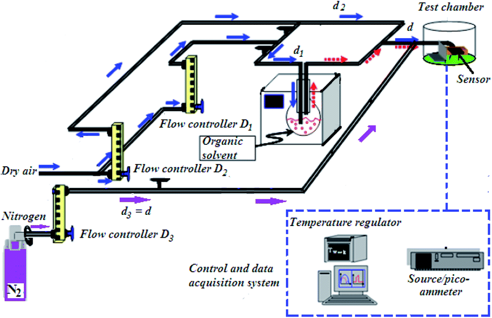 | ||
| Fig. 1 Experimental set-up for gas detection. | ||
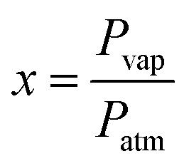
The global gas circuit has two sub-circuits. The first is used to test the organic vapor generated using two mass-flow controllers D1 and D2 which are used to set the dry air flow rate and the organic vapor concentration. The dry air from flow controller D1 is charged with vapor through a dilution bath containing a pure organic solvent. This latter is maintained at a fixed temperature in order to adjust the saturation vapor partial pressure. This flow is mixed with the second flow of dry air coming from the second flow controller D2. By varying d1 and d2 (d1 + d2 were kept constant at 1 L min−1), diverse concentrations of organic vapor can be obtained and computed using the formula:30,31
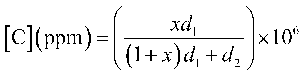 | (2) |
 | (3) |
The total flow charged with organic vapor has been blown on the sensor for 5 min. Then the test chamber has been purged with dry air for 15 min.
A second sub-circuit is used to check oxygen adsorption/desorption phenomenon. Since the test chamber is dynamic, the gases are controlled at 1 L min−1 flow rate. Nitrogen (0% oxygen atmosphere) is sent along the third arm D3. Firstly, the flow loaded with dry air (20% oxygen atmosphere) was sent along the second arm D2 and blown directly on the sensor for 5 min. Then, it was removed from the test chamber by switching the gas flow to nitrogen for 15 min.
Samples were polarized at 0.5 V. The measurements of direct current intensity have been done in real time using a (HP 4140B) Source/Picoammeter. The electrical contact on the sensor is ensured by gold tip tungsten electrodes. Measurements were done at different operating temperatures ranging from 150 °C to 425 °C. The sensor is heated by a halogen lamp which is powered by a stabilized generator and controlled by an (HP 34401A) Multimeter regulator that allows to set the temperature of the semiconductor by measuring the resistance across the RTD PT100 platinum probe that will be converted into a temperature value.
In order to compare the responses of In2S3 sensors we will use the following formula of sensing response:30,31
| Response = Ra/Rg | (4) |
3. Results and discussion
3.1. Characterization
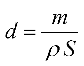 | (5) |
The obtained values of thicknesses for all samples are illustrated in Table 1 and show that thickness increases from 0.8 μm to 6.1 μm by rising deposit time in the range 10–90 min.
| Spray time (min) | Thickness (μm) | D (nm) | δ (1010 lines per cm−2) | Rq (nm) | Rsk |
|---|---|---|---|---|---|
| 10 | 0.8 | 39.1 | 6.5 | 141 | −0.35 |
| 30 | 2.3 | 43.1 | 5.2 | 207 | −0.27 |
| 50 | 3.2 | 51.7 | 3.7 | 223 | −0.22 |
| 70 | 4.8 | 52.1 | 3.7 | 501 | 0.93 |
| 90 | 6.1 | 41.3 | 5.8 | 1150 | 0.43 |
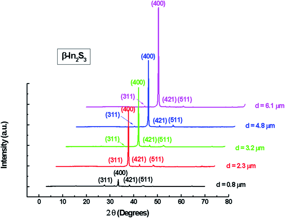
The X-ray diffraction patterns of the In2S3 layers obtained for different thicknesses are shown in Fig. 2.
 | ||
| Fig. 2 XRD patterns of sprayed In2S3 films. | ||
These patterns indicate that all films were polycrystalline and can be closely indexed to pure β-In2S3 phase with a simple cubic structure matching with the standard file of JCPDS 32-0456. The preferred orientation observed in the pattern for all samples is (400). The intensity of the diffraction main peak becomes more intense with the increase of spray time. Such behavior can be explained by the increase of film thickness and the increased ability of atoms to orient in proper equilibrium sites giving more preferentially oriented films.
The main peak was used to determine the crystallite size using Lorentzian fits and Scherrer's formula:32
 | (6) |
Likewise, the imperfection in the films can be quantified by computing the dislocation density (δ) which is defined as the length of dislocation lines per unit volume of the crystal. For the (400) peak, it was calculated using the Williamson–Smallman relation:33
 | (7) |
The interplanar d-spacing (dhkl) for In2S3 nanoparticles was calculated using Bragg's eqn (8). The lattice parameter (a) associated with dhkl and Miller indices (h,k,l) are calculated via the theoretical eqn (9) and (10) as well:32
 | (8) |
 | (9) |
| a = 4d400 | (10) |
The calculated lattice parameter reveals a constant value a = 10.7 Å, while crystallite size and dislocation density of films are presented in Table 1.
It can be seen that the change in thickness affects the density of native imperfections which modify the structural quality of the films. In fact, a maximum of the crystallite size (D = 52 nm) and a minimum of the defect δ (δ = 3.7 × 10¹⁰ lines per cm−2) is located around a thickness of 4.8 μm reflecting the best crystallinity of the deposit in this condition.
Fig. 3 presents 2D surface measurement of In2S3 samples over a scanned area of 1 mm2. In this case we arbitrarily amplify the z axis and we also know the altitudes using a color palette that allows appreciating the local variations of the heights. Here the variations of the relief are also amplified and the represented surfaces would appear flat. The surface roughness of films seems to change from one layer to another with a changing thickness.
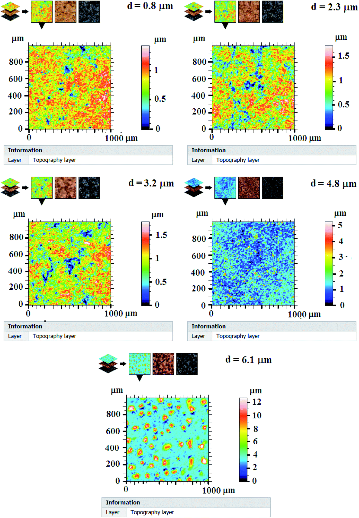 | ||
| Fig. 3 Topography images of In2S3 films. | ||
The parameters (prefix) R calculated on the roughness profile are defined in a handful of international standards Geometric Product Specifications (GPS) – Surface Texture: Profile Method (ISO 4287:1997). Some parameters calculated on segments of the profile (the base lengths) and averaged over several segments are presented in Table 1. These results are evaluated from measurements in three different areas of each sample and from five profiles for each area.
Rq, root mean squared roughness, is the standard deviation of the height distribution over the evaluation length. We can note from Table 1 that Rq increases eventually with increasing thickness by rising spray time and shows high values for samples matching thicknesses of 4.8 μm and 6.1 μm.
Rsk, asymmetry of the profile: asymmetry of the distribution of the heights, defined on the length of evaluation. This parameter is important because it gives information on the morphology of the surface state. A positive value of Rsk (thicknesses of 4.8 μm and 6.1 μm) corresponds to a surface having peaks and protuberances above the surface, and thus a distribution shifts towards the lowest points, while a negative value (thicknesses of 0.8 μm, 2.3 μm and 3.2 μm) corresponds to a plateau surface with scratches or deep pores, and a shifted distribution towards the highest points.
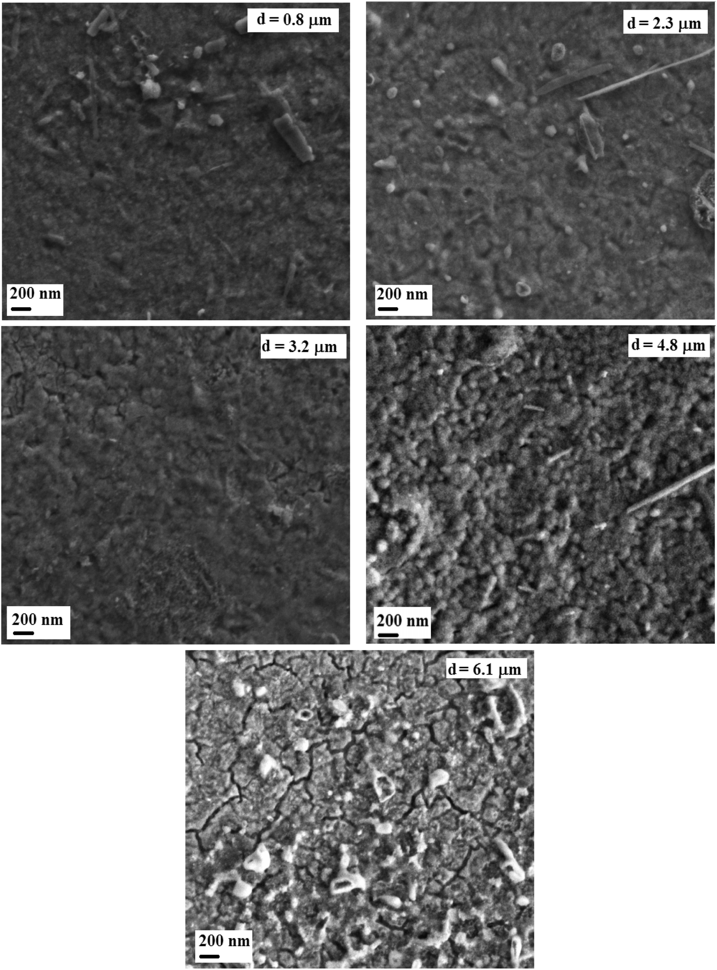
The morphological study by SEM shows in Fig. 4 the microscopic appearance of the surface layers for different thicknesses.
 | ||
| Fig. 4 SEM images of sprayed In2S3 films. | ||
The films were well covered, homogeneous, dense and continuous. We can note that the thickness effect is reflected on the film surface morphologies. SEM images reveal a granular layer for the sample corresponding to the thickness of 4.8 μm, whereas the layers are smooth for the others thicknesses. In addition to this, big granules/chunks are observed at the figure for 0.8 μm, 2.3 μm, and 4.8 μm thicknesses. Such observation may be a result of a small deviation from the stoichiometric composition in starting a solution that yields a very strong influence on the microstructure and the surface morphology of the films. This behavior was the subject of previous reports on films such as In2S3 (ref. 34) and CuInS2.35 We can also note a rougher layer surface with cracks at the higher thickness of 6.1 μm identifying a beginning of crystallinity degradation.
| Thickness (μm) | S (at%) | In (at%) | S/In |
|---|---|---|---|
| 0.8 | 31.60 | 23.68 | 1.33 |
| 2.3 | 37.83 | 30.15 | 1.25 |
| 3.2 | 37.98 | 29.90 | 1.27 |
| 4.8 | 36.92 | 29.07 | 1.27 |
| 6.1 | 35.74 | 28.92 | 1.24 |
These results are evaluated from measurements in four different areas of each sample. The S/In molar ratio remains constant for all the samples with an average value of 1.27. This order of magnitude is less than the stoichiometric ratio (S/In = 1.5) of the In2S3 material. This indicates that the prepared In2S3 material contains defective sulfur positions.
3.2 VOCs sensing properties
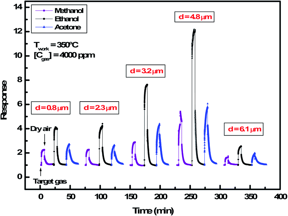 | ||
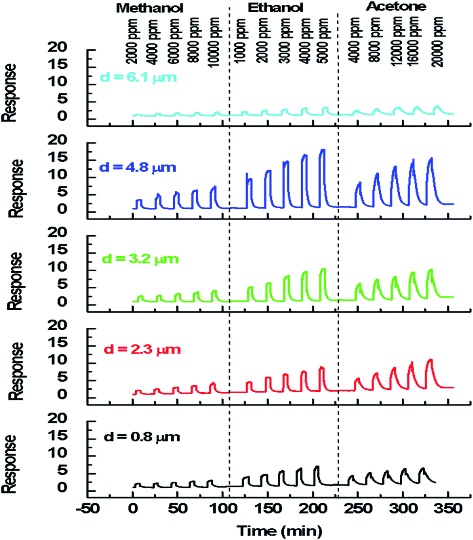
| Fig. 5 Dynamic response of In2S3 films to 4000 ppm of methanol, ethanol and acetone at 350 °C for thickness varying from 0.8 μm to 6.1 μm. | ||
We note that for all the prepared sensors, during the exposure to target gas, the response increases quickly to an equilibrium value and then returns to the baseline when dry air is re-injected in the test chamber. This behavior is consistent with the sensing mechanism of n-type semiconductors. It is also observed that the response plot obtained is affected by the change of thickness. A possible explanation is that samples have different specific surface areas. In the case of smooth layers and low roughness (d = 0.8 μm, d = 2.3 μm, d = 3.2 μm/root mean squared roughness of 141 nm, 207 nm and 223 nm, respectively) the gas interaction is only taking place at the geometric surface. In the case of granular layer and high roughness (d = 4.8 μm, Rq = 501 nm), the gas interaction can therefore take place at the surface of individual grains and at grain–grain boundaries.36 So, such sensor presents a higher specific surface area involving abundant active adsorption sites which improve the gas response. This result confirms the proposal to improve the response by changing microstructure and morphology of sensors.37 In the case of sample (d = 6.1 μm, Rq = 1150 nm) cracks increase the electric potential barriers, reduce the current and diminish the sensing response. Indeed, the increase in resistance is related to the number of cracks in the semiconductor layer which depends on the applied deformation and the thickness of the film.38 Despite the fact that the cracks can be the gas trapping path, it is also very possible that they cause an electrical rupture of these areas. We think that the active surface which describes the resistance decreases enormously with these cracks because they prevent the electrical contribution of a certain volume of material and therefore reduce the response of the sensor.
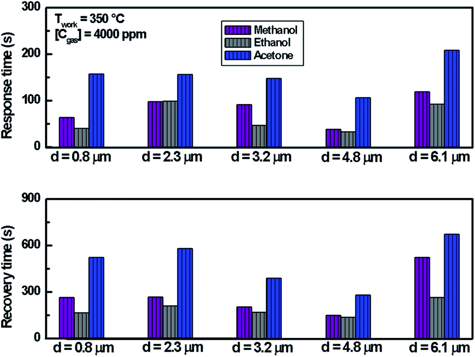 | ||
| Fig. 6 Response and recovery times of In2S3 films to 4000 ppm of methanol, ethanol and acetone at 350 °C. | ||
000 ppm, 1000 ppm to 5000 ppm and 4000 ppm to 20000 ppm respectively at the operating temperature of 350 °C. For each sensor, the sensor's response has an obvious increasing relationship with VOCs concentration, demonstrating that the sensor can offer more surface active sites and adsorb more VOCs molecules. Moreover, the sensor's response is affected by the layer's thickness and the best response was performed with the thickness matching 4.8 μm. This fact reflects the reproducibility of the results detailed previously.
 | ||
| Fig. 7 Dynamic response of In2S3 sensors with different thicknesses to various concentrations of methanol, ethanol and acetone at the operating temperature of 350 °C. | ||
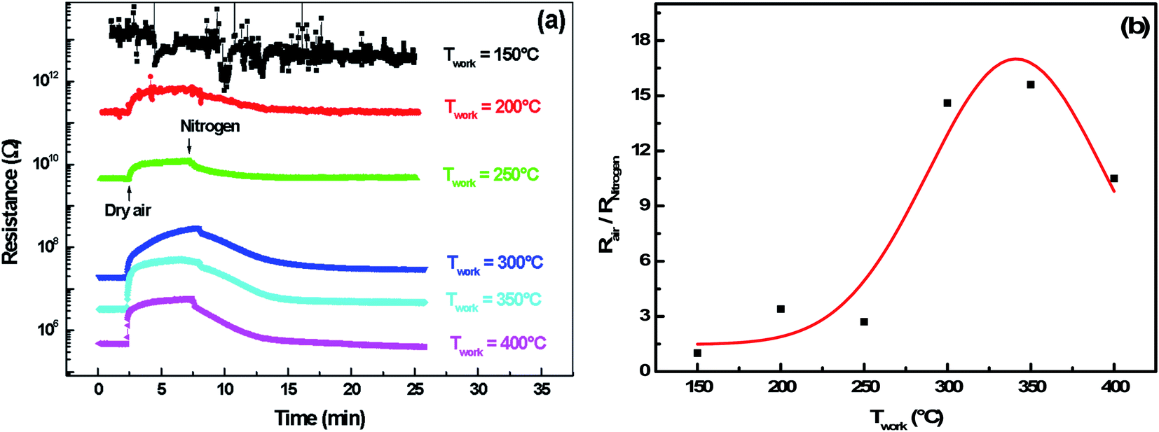
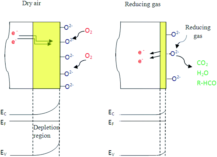
3.2.4.1 Oxygen adsorption/desorption. Here, the adsorption and desorption of oxygen on a polycrystalline indium sulfide thin layers have been experimentally demonstrated by performing alternating exposure to nitrogen and dry air at a working temperature ranging from 150 °C to 400 °C. Fig. 8(a) shows that resistance increases when dry air is introduced in the test chamber and decreases after its evacuation by nitrogen for an operating temperature higher than 200 °C.
 | ||
| Fig. 8 (a) Resistance change of In2S3 film with time upon altering exposure to dry air and nitrogen at operating temperature ranging from 150 °C to 400 °C, (b) response of In2S3 film to oxygen as a function of operating temperature. | ||
In fact, under dry air an adsorption phenomenon occurs. Ho et al.39 reported that because of sulfur vacancies and indium interstitials defects, the β-In2S3 crystal can form easily surface oxidation states of β-In2S3−3xO3x in ambient air (or O2) by chemical reaction of In–O. So, we think that the interaction of atmospheric oxygen with the surface of In2S3 forms a layer of charged oxygen species, which traps electrons from the bulk of the material. The electrons trapped for this process are removed from the conduction band and are confined on the surface.36 Consequently, a space charge layer is formed. The presence of negative surface charges leads to a band bending defined by potential barrier eVs at the surface. This restricts the electron flow and decreases the conductivity. On the other hand, under nitrogen, the resistance decreases reflecting the oxygen desorption phenomenon.
In this context, the study of the oxygen sensing response versus the operating temperature was illustrated in Fig. 8(b). The response increases by increasing the working temperature up to 350 °C and decreases above this temperature. This fact could be interpreted as a competition between the rates of oxygen adsorption and desorption, which is shown in the Lennard-Jones40 equation:
 | (11) |
3.2.4.2 Operating temperature effect. Fig. 9(a) demonstrates the resistance change during an alternating exposure to dry air and organic vapor (methanol, ethanol and acetone) at 4000 ppm concentration. Measurements were made at different operating temperatures in the range of 250–425 °C. The counting of these results is shown in Fig. 9(b).
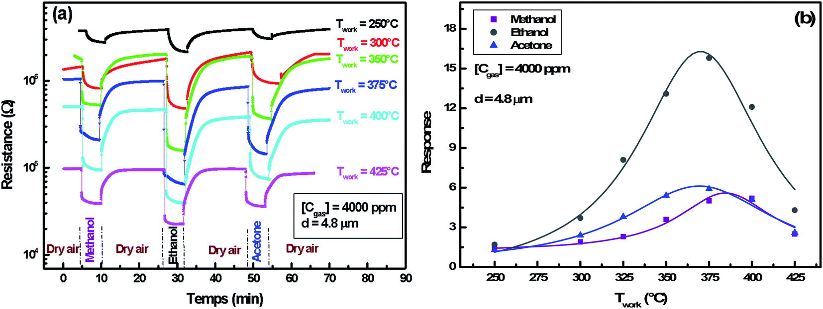 | ||
| Fig. 9 (a) Resistance evolution of In2S3 sensor upon exposure to 4000 ppm concentration of various organic vapors at operating temperatures in the range: 250–400 °C, (b) sensing response of In2S3 sensor vs. working temperature towards various organic vapors. | ||
The evolution of the response versus the working temperature follows also Lennard-Jones equation and shows an optimal temperature for each gas. It clearly shows a direct correlation between oxygen adsorption and reducing gas detection. Indeed, responses to oxygen and reducing gases present a similar evolution and a neighboring optimal temperature.
The increase in operating temperature before the optimum value improves the oxygen adsorption and hence the VOCs response. On the other hand, desorption of all oxygen ionic species previously adsorbed occurs at high temperatures, which explains the response decrease to reducing gases beyond the optimum value.
We note that optimal temperature for ethanol and acetone is 365 °C, whereas it is shifted to 385 °C for methanol gas. Similarly, such a trend has been studied by Bejaoui et al.41 They proposed a model simulating the interaction between sensors and reducing gases. They showed that the increase of the activation energy following a change of gas causes a shift of the optimal temperature towards a higher value. We also remarked that ethanol response (16.2) is higher than the acetone one (6.3) at the same optimal temperature. This could be explained by the ethanol and the acetone molecules' size difference. Indeed, the surface cover rate is higher for the smaller molecules of ethanol.
3.2.4.3 Gas concentration effect. In order to identify ionosorbed oxygen species, measurements were conducted on the In2S3 sensor at a working temperature of 350 °C by varying the concentration of methanol, ethanol and acetone. The transient current during cycles (air/reducing gas/air) is shown in Fig. 10(a). The fitting of the response (Sgas) versus gas concentration (Cgas) obtained in Fig. 10(b) shows a power law:
| Sgas = Cte [Cgas]γ | (12) |
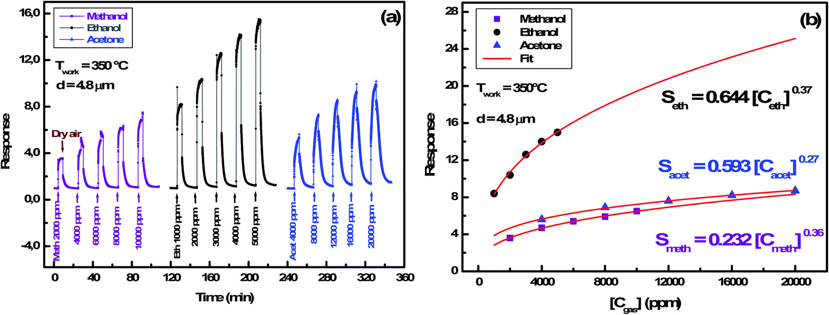 | ||
| Fig. 10 (a) Dynamic response of In2S3 sensor to various organic vapor concentrations at 350 °C, (b) experimental and power fit of sensing response of In2S3 sensor as a function of organic vapor concentration at 350 °C. | ||
Thus, ionization equations of adsorbed oxygen can be written as follows:
| O2(gas) → O2(ads) | (13) |
| O2(ads) + 4e− → 2O(ads)2− | (14) |
In the same context, when the material is exposed to reducing gases, the organic molecules are oxidized by oxygen species O2− and simultaneously the electrons are fed back into sensing body, the potential barrier is reduced and the conductivity increases. This mechanism can be expressed as follows:
| For methanol: CH3OH(ads) + O(ads)2− → H2CO(gas) + H2O + 2e− | (15) |
| For ethanol: C2H5OH(ads) + O(ads)2− → CH3CHO(gas) + H2O + 2e− | (16) |
| For acetone: CH3COCH3(ads) + 8O(ads)2− → 3CO2(gas) + 3H2O(gas) + 16e− | (17) |
So, oxygen plays the main element in reducing gas sensing response as detailed by the mechanism presented in Fig. 11.
 | ||
| Fig. 11 Detection mechanism of organic vapor by In2S3 sensor. | ||
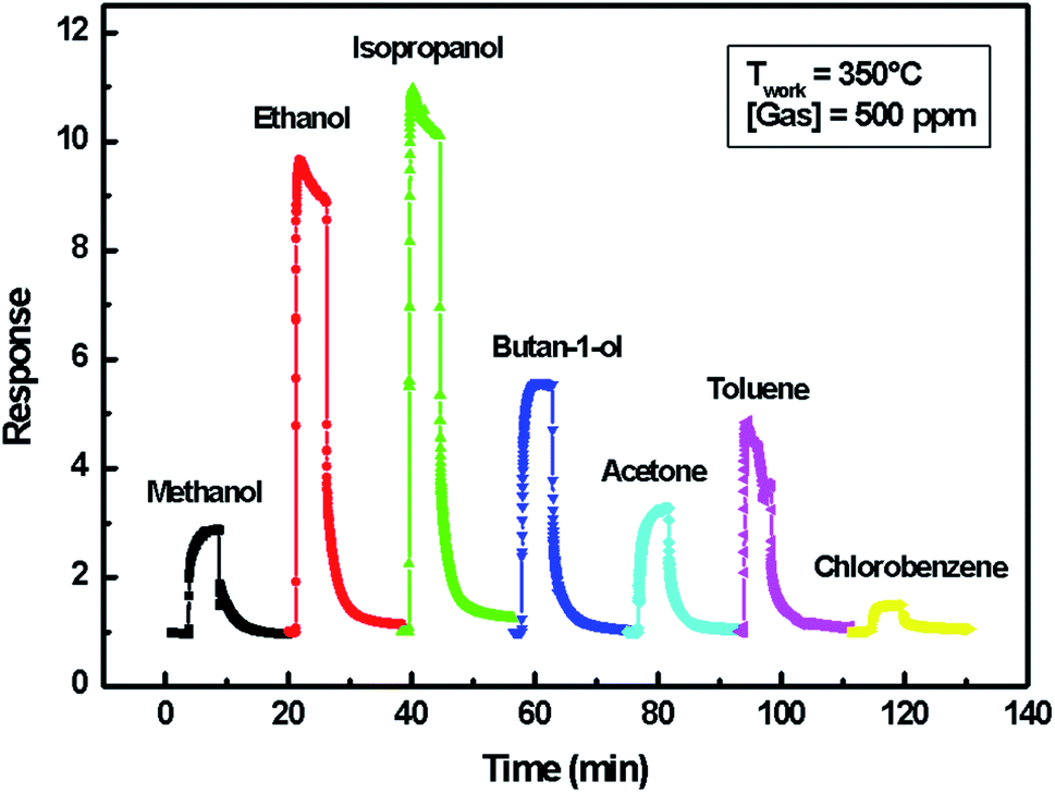 | ||
| Fig. 12 Selectivity of In2S3 sensor (d = 4.8 μm). | ||
A comparison of the developed sensor response to those of previously published indium oxide sensors is reported in Table 3. The results show that the ethanol detection response of indium sulfide In2S3-based sensor in the present work is not high but can be improved by enhancing gas adsorption or promoting specific chemical reactions via catalytic or electronic effects using bulk dopants and by the addition of metallic clusters or oxide catalysts.44–46
| Material | Ethanol concentration (ppm) | Response | τres/τrec (s) | Topt (°C) | Reference |
|---|---|---|---|---|---|
| In2S3 | 500 | 9.5 | 23/75 | 350 | This work |
| In2S3 | 500 | 1.7 | 150/155 | 350 | 30 |
| In2O3 | 50 | 5 | 40/38 | 300 | 47 |
| 3% Ag-doped In2O3 | 50 | 30 | 32/140 | 300 | 47 |
| In2O3/Au NRs | 500 | 320 | —/— | 400 | 48 |
| In2O3 hierarchical architecture | 100 | 1.5 | —/— | 260 | 49 |
| In2O3 microcubes | 500 | 55 | —/— | 210 | 50 |
| Ce-doped In2O3 | 100 | 27.8 | —/— | 240 | 51 |
| Pb-doped In2O3 | 100 | 32.5 | 2.2/0.7 | 250 | 52 |
4. Conclusion
In2S3 films were deposited on glass substrates by spray pyrolysis technique. Film thickness increases from 0.8 μm to 6.1 μm by increasing deposit time from 10 min to 90 min. XRD diffraction analysis reveals the formation of cubic ®-In2S3 pure phase with (400) preferred orientation. The crystallite size varies in the narrow 39–52 nm range. The EDS measurements indicate that the S/In molar ratio remains constant for all the samples with an average value of 1.27. The morphological study by SEM shows that films were well covered, homogeneous and dense. The parameter Rq calculated from the roughness profile increases eventually with increasing thickness. Thus, the In2S3 sample matching the thickness of 4.8 μm combine high roughness and best crystallinity. Such results were correlated with its best sensing properties. We have fairly improved the In2S3 sensor performances compared to that mentioned in the previous publication.30 The response to 500 ppm ethanol at 350 °C is enhanced from 1.7 to 9.5. The response time and recovery time are improved from 150 s/155 s to 23 s/75 s respectively. The optimal working temperature is found to be around 385 °C for methanol and 365 °C for both ethanol and acetone. Besides, oxygen adsorption versus working temperature were put forth and the sensing mechanism of the In2S3 semiconductor was explained on the bases of the reaction between the reducing vapors with the chemisorbed oxygen ions O2−. Nevertheless, these results revealing the potential of β-In2S3 in gas detection are encouraging for deepening the study in order to improve sensing properties and to test other gasses.Conflicts of interest
There are no conflicts to declare.Acknowledgements
This work was supported by Tunisian Ministry of Higher Education and Scientific Research, Spanish Ministry of Science and Innovation – FEDER Funds (MODENA Project CTQ2016-79461-R) and Fundación Ramón Areces (Spain, Project CIVP18A3940). NANOMAG group belongs to Galician Competitive Research Group ED431C-2017/22, programme co-funded by FEDER, and AEMAT Strategic Partnership (ED431E-2018/08, Xunta de Galicia, Spain). The authors are grateful to Dr N. Ihzaz (High Institute of Applied Sciences and Technology, Gabes University, Tunisia) for useful discussions.References
- B. Lawson, K. Aguir, T. Fiorido, V. Martini-Laithier, R. Bouchakour, S. Burtey, Ch. Reynard-Carette and M. Bendahan, Skin alcohol perspiration measurements using MOX sensors, Sens. Actuators, B, 2019, 280, 306–312 CrossRef CAS.
- Q. Rong, Y. Zhang, T. Lv, K. Shen, B. Zi, Z. Zhu, J. Zhang and Q. Liu, Highly selective and sensitive methanol gas sensor based on molecular imprinted silver doped LaFeO3 core–shell and cage Structures, Nanotechnology, 2018, 29, 145503–145511 CrossRef PubMed.
- Y. Xiong, Z. Zhu, D. Ding, W. Lu and Q. Xue, Multi-shelled ZnCo2O4 yolk-shell spheres for high-performance acetone gas sensor, Appl. Surf. Sci., 2018, 443, 114–121 CrossRef CAS.
- X. Li, D. Lu, C. Shao, G. Lu, X. Li and Y. Liu, Hollow CuFe2O4/α-Fe2O3 composite with ultrathin porous shell for acetone detection at ppb levels, Sens. Actuators, B, 2018, 258, 436–446 CrossRef CAS.
- O. Lupan, V. Postica, J. Gröttrup, A. K. Mishra, N. H. de Leeuw, J. F. C. Carreira, J. Rodrigues, N. Ben Sedrine, M. R. Correia, T. Monteiro, V. Cretu, I. Tiginyanu, D. Smazna, Y. K. Mishra and R. Adelung, Hybridization of zinc oxide tetrapods for selective gas sensing applications, ACS Appl. Mater. Interfaces, 2017, 9(4), 4084–4099 CrossRef CAS PubMed.
- E. Wongrat, N. Chanlek, C. Chueaiarrom, W. Thupthimchun, B. Samransuksamer and S. Choopun, Acetone gas sensors based on ZnO nanostructures dectorated with Pt and Nb, Ceram. Int., 2017, 43, 557–566 CrossRef.
- L. Zhu, Y. Li and Z. Wen, Hydrothermal synthesis of hierarchical flower-like ZnO nanostructure and its enhanced ethanol gas-sensing properties, Appl. Surf. Sci., 2018, 427, 281–287 CrossRef CAS.
- M. Asgari, F. H. Saboor, Y. Mortazavi and A. K. Khodadadi, SnO2 decorated SiO2 chemical sensors: enhanced sensing performance toward ethanol and acetone, Mater. Sci. Semicond. Process., 2018, 68, 87–96 CrossRef.
- A. Gaiardo, B. Fabbri, V. Guidi, P. Bellutti, A. Giberti, S. Gherardi, L. Vanzetti, C. Malagù and G. Zonta, Metal Sulfides as Sensing Materials for Chemoresistive Gas Sensors, Sensors, 2016, 16, 296–314 CrossRef PubMed.
- T. T. John, M. Mathew, C. S. Kartha, K. P. Vijayakumar, T. Abe and Y. Kashiwaba, CuInS2/In2S3 thin film solar cell using spray pyrolysis technique having 9.5% efficiency, Sol. Energy Mater. Sol. Cells, 2005, 89, 27–36 CrossRef CAS.
- M. Kraini, N. Bouguila, I. Halidou, A. Timoumi and S. Alaya, Properties of In2O3 films obtained by thermal oxidation of sprayed In2S3, Mater. Sci. Semicond. Process., 2013, 16, 1388–1396 CrossRef CAS.
- P. G. S. Abadi, M. S. Niasari and F. Davar, Hydrothermal synthesis, characterization and optical properties of 3D flower like indium sulfide nanostructures, Superlattices Microstruct., 2013, 53, 76–88 CrossRef.
- Z. Li, X. Tao, Z. Wu, P. Zhang and Z. Zhang, Preparation of In2S3 nanoparticle by ultrasonic dispersion and its tribology property, Ultrason. Sonochem., 2009, 16, 221–225 CrossRef CAS PubMed.
- B. Asenjo, C. Sanz, C. Guillén, A. M. Chaparro, M. T. Gutiérrez and J. Herrero, Indium sulfide buffer layers deposited by dry and wet methods, Thin Solid Films, 2007, 515, 6041–6044 CrossRef CAS.
- A. Timoumi, H. Bouzouita, M. Kanzari and B. Rezig, Fabrication and characterization of In2S3 thin films deposited by thermal evaporation technique, Thin Solid Films, 2005, 480, 124–128 CrossRef.
- B. Tiss, M. Erouel, N. Bouguila, M. Kraini and K. Khirouni, Effect of silver doping on structural and optical properties of In2S3 thin films fabricated by chemical pyrolysis, J. Alloys Compd., 2019, 771, 60–66 CrossRef CAS.
- N. Bouguila, M. Kraini, I. Halidou, E. Lacaze, H. Bouchriha and H. Bouzouita, Thickness effect on properties of sprayed In2S3 films for photovoltaic applications, J. Electron. Mater., 2016, 45, 829–838 CrossRef CAS.
- N. Bouguila, M. Kraini, A. Timoumi, I. Halidou, C. Vázquez-Vázquez, M. A. López Quintela and S. Alaya, Substrate temperature effect on properties of sprayed In2S3 films, J. Mater. Sci.: Mater. Electron., 2015, 26, 7639–7648 CrossRef CAS.
- T. Schulmeyer, A. Klein, R. Kneiese and M. Powalla, Band offset at the CuGaSe2/In2S3 heterointerface, Appl. Phys. Lett., 2004, 85, 961–963 CrossRef CAS.
- R. Diehl and R. Nitsche, Vapour growth of three In2S3 modifications by iodine transport, J. Cryst. Growth, 1975, 28, 306 CrossRef CAS.
- J. Sterner, J. Malmstrom and L. Stolt, Study on ALD In2S3/Cu(In,Ga)Se2 interface formation, Prog. Photovoltaics, 2005, 13, 179 CAS.
- S. Buecheler, D. Corica, D. Guettler, A. Chirila, R. Verma, U. Muller, T. P. Niesen, J. Palm and A. N. Tiwari, Ultrasonically sprayed indium sulfide buffer layers for Cu(In,Ga)(S,Se)2 thin-film solar cells, Thin Solid Films, 2009, 517, 2312–2315 CrossRef CAS.
- E. Dalas and L. Kobotiatis, Primary solid-state batteries constructed from copper and indium sulphides, J. Mater. Sci., 1993, 28, 6595 CrossRef CAS.
- Yu-J. Hsiao, C.-H. Lu, L.-W. Ji, T.-H. Meen, Y.-L. Chen and H.-P. Chi, Characterization of photovoltaics with In2S3 nanoflakes/p-Si heterojunction, Nanoscale Res. Lett., 2014, 9, 32–38 CrossRef PubMed.
- D. K. Nagesha, X. Liang, A. A. Mamedov, G. Gainer, M. A. Eastman, M. Giersig, J. J. Song, T. Ni and N. A. Kotov, In2S3 Nanocolloids with Excitonic Emission: In2S3 vs. CdS Comparative Study of Optical and Structural Characteristics, J. Phys. Chem. B, 2001, 105, 7490 CrossRef CAS.
- B. Hemanth Kumar and M. C. Santhosh Kumar, Indium sulfide based metal-semiconductor-metal ultraviolet-visible photodetector, Sens. Actuators, A, 2019, 299, 111643 CrossRef.
- R. A. Ismail, N. F. Habubi and M. M. Abbod, Preparation of high-sensitivity In2S3/Si heterojunction photodetector by chemical spray pyrolysis, Opt. Quantum Electron., 2016, 48, 455–468 CrossRef.
- S. Ghosh, M. Saha, V. D. Ashok, A. Chatterjee and S. K. De, Excitation dependent multicolor emission and photoconductivity of Mn, Cu doped In2S3 monodisperse quantum dots, Nanotechnology, 2016, 27, 155708–155724 CrossRef PubMed.
- P. Cai, H. Song and Y. Lva, Hierarchical spheres In2S3-based cataluminescence sensor for ammonium sulfide, Microchem. J., 2018, 138, 116–121 CrossRef CAS.
- R. Souissi, N. Bouguila and A. Labidi, Ethanol sensing properties of sprayed ®-In2S3 thin films, Sens. Actuators, B, 2018, 261, 522–530 CrossRef CAS.
- A. Labidi, E. Gillet, R. Delamare, M. Maaref and K. Aguir, Ethanol and ozone sensing characteristics of WO3 based sensors activated by Au and Pd, Sens. Actuators, B, 2006, 120, 338–345 CrossRef CAS.
- B. D. Cullity, Elements of X-ray Diffraction, Addison-Wesley, Reading, MA, 1978, Library of Congress Catalog Card No. 77-73950, ISBN 0-201-01174-3 Search PubMed.
- V. Bilgin, S. Kose, F. Atay and I. Akyuz, The effect of substrate temperature on the structural and some physical properties of ultrasonically sprayed CdS films, Mater. Chem. Phys., 2005, 94, 103–108 CrossRef CAS.
- N. Revathi, P. Prathap and K. T. Ramakrishna Reddy, Synthesis and physical behavior of In2S3 films, Appl. Surf. Sci., 2008, 254, 5291–5298 CrossRef CAS.
- M. Krunks, O. Bijakina, T. Varema, V. Mikli and E. Mellikov, Structural and optical properties of sprayed CuInS2 films, Thin Solid Films, 1999, 338, 125–130 CrossRef CAS.
- N. Barsan and U. Weimar, Conduction model of metal oxide gas sensors, J. Electroceram., 2001, 7, 143–167 CrossRef CAS.
- A. Dey, Semiconductor metal oxide gas sensors: a review, Mater. Sci. Eng., B, 2018, 229, 206–217 CrossRef CAS.
- D. R. Cairns, R. P. Witte, D. K. Sparacin, S. M. Sachsman, D. C. Paine, Gr. P. Crawford and R. R. Newton, Electric resistance dependent on the stress of indium oxide doped with tin on polymeric substrates, Appl. Phys. Lett., 2000, 76(11), 1425 CrossRef CAS.
- C. Ho, M. Lin, Y. Wang and Y. Huang, Synthesis of In2S3 and Ga2S3 crystals for oxygen sensing and UV photo-detection, Sens. Actuators, A, 2016, 245, 119–126 CrossRef CAS.
- A. Labidi, C. Jacolin, M. Bendahan, A. Abdelghani, J. Guérin, K. Aguir and M. Maaref, Impedance spectroscopy on WO3 gas sensor, Sens. Actuators, B, 2005, 106, 713–718 CrossRef CAS.
- A. Bejaoui, J. Guerin and K. Aguir, Modeling of a p-type resistive gas sensor in the presence of a reducing gas, Sens. Actuators, B, 2013, 181, 340–347 CrossRef CAS.
- X. Vanden Eynde and P. Bertrand, ToF-SIMS quantification of polystyrene spectra based on principal component analysis (PCA), Surf. Interface Anal., 1997, 25, 878–888 CrossRef.
- M. Penza, G. Cassano and F. Tortorella, Gas recognition by activated WO3 thin film sensors array, Sens. Actuators, B, 2001, 81, 115–121 CrossRef CAS.
- L. Liu, P. Song, Z. Yang and Q. Wang, Ultra-fast responding C2H5OH sensors based on hierarchical assembly of SnO2 nanorods on cube-like α-Fe2O3, J. Mater. Sci.: Mater. Electron., 2018, 29(7), 5446–5453 CrossRef CAS.
- P. Tyagi, A. Sharma, M. Tomar and V. Gupta, Metal oxide catalyst assisted SnO2 thin film based SO2 gas sensor, Sens. Actuators, B, 2016, 224, 282–289 CrossRef CAS.
- D. Hohl, The role of noble metals in the chemistry of solid-state gas sensors, Sens. Actuators, B, 1990, 1, 158–165 CrossRef.
- K. Anand, J. Kaur, R. C. Singh and R. Thangaraj, Preparation and characterization of Ag-doped In2O3 nanoparticles gas Sensor, Chem. Phys. Lett., 2017, 682, 140–146 CrossRef CAS.
- R. Xing, L. Xu, J. Song, C. Zhou, Q. Li, D. Liu and H. W. Song, Preparation and gas sensing properties of In2O3/Au nanorods for detection of volatile organic compounds in exhaled breath, Sci. Rep., 2015, 5, 10717–10730 CrossRef CAS PubMed.
- S. Wang, J. Cao, W. Cui, L. Fan, X. Li and D. Li, Oxygen vacancies and grain boundaries potential barriers modulation facilitated formaldehyde gas sensing performances for In2O3 hierarchical architectures, Sens. Actuators, B, 2018, 255, 159–165 CrossRef CAS.
- X. Zhou, F. Qu, B. Zhang, C. Jiang and M. Yang, Facile synthesis of In2O3 microcubes with exposed {100} facets as gas sensing material for selective detection of ethanol vapor, Mater. Lett., 2017, 209, 618–621 CrossRef CAS.
- X. Liu, L. Jiang, X. Jiang, X. Tian, X. Sun, Y. Wang, W. He, P. Hou, X. Deng and X. Xu, Synthesis of Ce-doped In2O3 nanostructure for gas sensor applications, Appl. Surf. Sci., 2018, 428, 478–484 CrossRef CAS.
- A. Montazeri and F. Jamali-Sheini, Enhanced Ethanol Gas-Sensing Performance of Pb-Doped In2O3 Nanostructures Prepared by Sonochemical Method, Sens. Actuators, B, 2017, 242, 778–791 CrossRef CAS.
| This journal is © The Royal Society of Chemistry 2020 |