
 Open Access Article
 This Open Access Article is licensed under a Creative Commons Attribution-Non Commercial 3.0 Unported Licence
Epitaxial and large area Sb2Te3 thin films on silicon by MOCVD†
Martino Rimoldi a,
Raimondo Cecchinia,
Claudia Wiemera,
Alessio Lampertia,
Emanuele Longoab,
Lucia Nasic,
Laura Lazzarinic,
Roberto Mantovan*a and
Massimo Longo*a
a,
Raimondo Cecchinia,
Claudia Wiemera,
Alessio Lampertia,
Emanuele Longoab,
Lucia Nasic,
Laura Lazzarinic,
Roberto Mantovan*a and
Massimo Longo*a
aInstitute for Microelectronics and Microsystems, CNR-IMM Unit of Agrate Brianza, Via C. Olivetti 2, 20864, Agrate Brianza, Italy. E-mail: massimo.longo@mdm.imm.cnr.it; roberto.mantovan@mdm.imm.cnr.it
bUniversity of Milano-Bicocca, Department of Material Science, Via R. Cozzi 55, 20126, Milan, Italy
cInstitute of Materials for Electronics and Magnetism, CNR-IMEM, Parma, Parco Area delle Scienze, 7/A, 43100 Parma, Italy
First published on 27th May 2020
Abstract
Antimony telluride (Sb2Te3) thin films were prepared by a room temperature Metal–Organic Chemical Vapor Deposition (MOCVD) process using antimony chloride (SbCl3) and bis(trimethylsilyl)telluride (Te(SiMe3)2) as precursors. Pre-growth and post-growth treatments were found to be pivotal in favoring out-of-plane and in-plane alignment of the crystallites composing the films. A comprehensive suite of characterization techniques were used to evaluate their composition, surface roughness, as well as to assess their morphology, crystallinity, and structural features, revealing that a quick post-growth annealing triggers the formation of epitaxial-quality Sb2Te3 films on Si(111).
Introduction
Chalcogenide structures, such as two-dimensional layered materials,1 thin films,2–4 and nanowires,5–7 recently have become technologically relevant materials in the context of memory devices and spintronics.8In particular, the semiconductor antimony telluride (Sb2Te3) has been exploited in phase change memory cells, taking advantage of its reversible amorphous-to-crystalline transition,9,10 as a thermoelectric material,11–13 and more recently as a topological insulator (TI),14,15 since it has been demonstrated, despite its insulating bulk, to possess surface Dirac cones and conductive edge states.
So far, various techniques have been reported capable of Sb2Te3 deposition, including microwave-assisted solvothermal synthesis,16 sputtering,17,18 chemical vapor deposition,19,20 atomic layer deposition,12,21–26 molecular beam epitaxy,27–30 and Metal–Organic Chemical Vapor Deposition (MOCVD).31–39
Amongst these methods, MOCVD, an industrially ready technique historically adopted for large-scale semiconductor production and suitable for large area film growth, appears to be the preferred scale-up option in an industrial environment. The quality of the films is fundamental for their use in electronic applications. Crystalline and highly oriented materials are required to exploit their physical properties and to achieve a successful device implementation, as demonstrated for instance in the variety of successful III–V semiconductors-based devices40,41—the ultimate target being epitaxy and single crystal growth.
Epitaxial films of Sb2Te3 (and other topological insulators such as Bi2Te3 and Bi2Se3) have been straightforwardly grown by molecular beam epitaxy processes,29,30 a technique that shows its limits in the volume production. On the other hand, chemical vapor deposition techniques suffer from poor morphology control, and we specifically investigated MOCVD with this regard.
Commonly employed substrates in TIs growth, such as Si(100), Si(111), and Al2O3(0001), show a significant lattice mismatch with Sb2Te3 (and TIs in general) that therefore grows as poorly oriented polycrystalline layers in the presence of rotational domains,23,32–34 with only a few exceptions.42,43 Recently, to overcome this issue, way less common materials, such as BaF2(111)30 and, for instance, a ZnTe or GaN buffer layer on Al2O3(0001), have been identified to lattice match with telluride-TIs and effectively adopted as substrates to enhance the quality of the films.30,35 Most significantly, the large area deposition of high-quality Sb2Te3 epitaxial layers on Si substrates with thickness control below 100 nm would be much attractive for integration in CMOS compatible devices.
Specific to MOCVD processes, alike other chemical methods, the selection of precursors plays a relevant role in governing the growth and morphology of the films.
So far, the most promising results in Sb2Te3 growth were achieved employing trialkylstibines (such as SbMe3, SbiPr3) and diallyltellanes (TeEt2, TeiPr2) as precursors; however, temperatures greater than or equal to 400 °C were required, along with a dihydrogen partial pressure, to sustain the precursors' pyrolysis.32,35 The more engineered species Et2Te2![[thin space (1/6-em)]](https://www.rsc.org/images/entities/char_2009.gif) 34,44 and (Et2Sb)2Te33 have also been adopted for high-temperature depositions. Nevertheless, the high deposition rate required to achieve a uniform and well-oriented crystalline Sb2Te3 MOCVD resulted in films several hundreds of nanometers thick.34,35
34,44 and (Et2Sb)2Te33 have also been adopted for high-temperature depositions. Nevertheless, the high deposition rate required to achieve a uniform and well-oriented crystalline Sb2Te3 MOCVD resulted in films several hundreds of nanometers thick.34,35
Here, we report a room temperature (RT) MOCVD process to obtain epitaxial Sb2Te3 thin (30 nm) films on bare Si(111) substrates and show the effect of pre-growth (substrates annealing) and post-growth (film processing) treatments on the film morphology, surface roughness, crystallinity, and crystallographic orientation.
Experimental
Materials
The Si(111) substrates were purchased from Silicon Materials Inc. and cut in approximately 1–2 square centimeter pieces.Sb2Te3 thin films by MOCVD
Prior to deposition, the Si(111) substrates were treated with HF (5% in deionized H2O) for 3 min, thoroughly rinsed with deionized H2O, and N2-dried. Then, samples were quickly loaded into the glove box-protected MOCVD chamber. Sb2Te3 thin films were grown with an Aixtron AIX 200/4 MOCVD tool equipped with an IR-heated 4′′ rotating graphite susceptor. Electronic grade precursors antimony chloride (SbCl3) and bis(trimethylsilyl)telluride (Te(SiMe3)2) were supplied by Air Liquide Electronics. Precursors were loaded into bubblers thermalized at 20.0 (±0.1) °C and delivered to the MOCVD chamber through the vapor-saturated ultra-pure N2 carrier gas. Depositions were carried out at 25 °C for 90 min at 15 mbar pressure, with a total flow of 5.575 l min−1, and setting the precursors vapor pressures at 2.28 and 3.32 × 10⁻⁴ mbar for SbCl3 and Te(SiMe3)2, respectively. Substrates annealing (prior to deposition) was performed in situ at 500 °C for 60 min at 20 mbar, with a total N2 flow of 11.000 l min−1. Post-growth films annealing was performed in situ according to the following routine: (1) heating ramp: 5.575 l min−1 N2 flow, 900 mbar, from RT to 300 °C in 10 min; (2) annealing: 5.575 l min−1 N2 flow, 900 mbar, 300 °C, 15 min; (3) cooling ramp: 1.500 l min−1 N2 flow, 990 mbar, from 300 °C to 200 °C in 20 min, from 200 °C to 100 °C in 35 min, from 100 °C to 50 °C in 20 min.Materials characterization
Scanning Electron Microscopy (SEM) images were acquired on a ZEISS Supra 40 field emission scanning electron microscope at an acceleration voltage of 15 kV. Samples were cut prior to measurement and cross-section images collected at a tilting angle of 25°. Atomic Force Microscopy (AFM) images were obtained on a Bruker Dimension Edge instrument in non-contact mode using a sharp silicon AFM probe (TESPA, Bruker) with a typical radius of curvature in the 8–12 nm range. A polynomial background correction was applied to the raw data. Surface roughness is reported as Root Mean Square roughness (RMS roughness, Rq) and expressed in nanometers. Transmission Electron Microscopy (TEM) analyses were performed using a JEOL 2200FS microscope working at 200 kV equipped with an Energy Dispersive X-ray Spectrometer (EDX), two high-angle annular dark-field (HAADF) detectors and an in-column energy (Omega) filter. The cross-sectional view samples were prepared using standard mechano-chemical procedures and finished by ion beam thinning. Total reflection X-ray Fluorescence (TXRF) measurements were performed using an X-ray total reflection spectrometer equipped with a Mo Kα radiation source. Elemental composition of the Sb2Te3 films was determined from the ratio of the antimony and tellurium Lα lines (Sb Lα = 3.604 keV; Te Lα = 3.768 keV). X-Ray Photoelectron Spectroscopy (XPS) data were collected on a PHI 5600 instrument (monochromatic Al Kα X-ray source, 1486.6 eV) equipped with a concentric hemispherical analyzer. After the deposition, samples were quickly transferred from the MOCVD tools into the XPS loading chamber (approximately 5 seconds of air exposure) and the spectra acquired at a 45° take-off angle. The spectra were referenced to the C 1s signal set at 284.8 eV. Te and Sb 3d and 4d spectra were recorded. X-Ray Reflectivity (XRR) and X-ray Diffraction (XRD) pattern were acquired with a HRXRD IS2000 equipped with a Cu Kα radiation source, a four circle goniometer, and a curved 120° position-sensitive detector (Inel CPS-120).Results and discussion
The metal–organic chemical vapor deposition of antimony telluride thin films was developed at room temperature and under inert atmosphere (no dihydrogen required) taking advantage of the precursors' reactivity previously demonstrated in tellurides atomic layer deposition21–23 and in other similar CVD processes.45,46 Under the optimal growth conditions (SbCl3 and Te(SiMe3)2 partial pressures of 2.23 and 3.25 × 10⁻⁴ mbar, respectively, a total flow of 5.575 l min−1, a deposition pressure of 15 mbar, and a deposition time of 90 min) the process afforded on HF-treated Si(111) an approximately 30 nm thick continuous film.The Sb2Te3 films, referred to as “Sb2Te3 – As Deposited” (1), even though continuous, exhibited a marked granularity and a non-uniform grains orientation (Fig. 1), features reminiscent of the recently reported Sb2Te3 MOCVD on SiO2.37,38 Despite highly granular in nature, film 1 showed good grains cohesion resulting in a continuous film. AFM images substantiated a non-directional growth and a RMS roughness around 4–4.5 nm (range of values resulted from the evaluation of various AFM images).
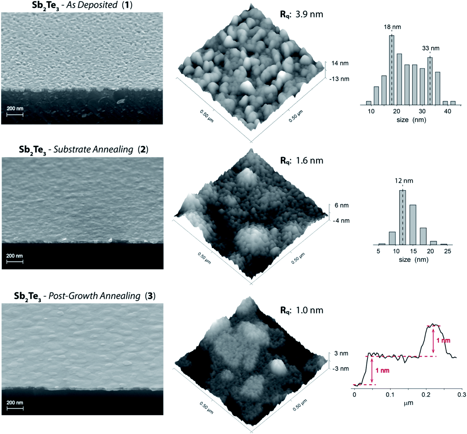 | ||
| Fig. 1 (Left) Tilted cross-section SEM images, (center) AFM images (Rq values are specific to the shown AFM images), (Right) grains size distribution histograms (as determined by AFM) of Sb2Te3 – As Deposited (1) and Sb2Te3 – Substrate Annealing (2), and a selected AFM surface profile of Sb2Te3 – Post-Growth Annealing (3). See ESI (Fig. S1–S8†) for more SEM and AFM images. | ||
In order to improve the film quality, we tested an in situ Si(111) substrate thermal annealing (500 °C and 20 mbar under N2 atmosphere for 1 h). Tilted cross-section SEM images of Sb2Te3 films deposited on the treated substrate (“Sb2Te3 – Substrate Annealing”, 2) clearly showed a film of enhanced crystallinity and significantly improved morphology; granularity was largely diminished to the extent that Sb2Te3 appeared as a continuous film no longer composed of juxtaposed grains of various sizes and, consequently, the surface roughness was lowered (RMS roughness of 1.5–1.8 nm) (Fig. 1).
AFM data highlighted interesting features in the fine structure of the films (Fig. 1). Sb2Te3 – As Deposited (1) exhibited a non-uniform granularity consisting of a bimodal grains size distribution centered at ca. 18 and 33 nm. On the other hand, the Sb2Te3 – Substrate Annealing (2) film could be described by a narrower distribution of smaller grains – mostly within the 11–14 nm range – specifically accountable for the lower surface roughness.
Aiming at further structural improvement, we performed an in situ post-growth treatment; the Sb2Te3 film 2 was subjected to a thermal annealing at 300 °C under N2 atmosphere for 15 min, at a relatively high pressure (900 mbar) to prevent or minimize desorption phenomena (Fig. 1, “Sb2Te3 – Post-Growth Annealing”, 3). This post-growth processing step neither did alter the film thickness nor was detrimental to its uniformity. It triggered instead a reorganization of the grains throughout the film. Nevertheless, the most relevant feature happened to be the film orientation that, as qualitatively ascertained from SEM and AFM images, became highly uniform and well-defined, along with a further lowering of the roughness (RMS roughness of 0.9–1.3 nm). An AFM profile extracted from Sb2Te3 – Post-Growth Annealing (3) (Fig. 1) evidences steps of 1 nm (consistent with an antimony telluride quintuple layer), supporting an improved ordering with respect to the parent Sb2Te3 materials 1 and 2.
The MOCVD average growth rate of 0.44 ± 0.01 nm min−1, extrapolated from films prepared with different deposition times, resulted appreciably lower than literature values that fall within the 8–50 nm min−1 range.33–35,45 However, dissimilar experimental conditions, including the choice of the precursors (their chemical reactivity), the higher deposition temperature (up to 450 °C), and the use of dihydrogen rather than an inert gas, can significantly impact the growth rate and are therefore accountable for the observed low values.
The morphology and structural properties of the films were studied in detail by performing TEM analyses. Typical cross-sectional high-resolution views of the three different types of samples are reported in Fig. 2, including the corresponding Fast Fourier Transform (FFT) (insets). In general, crystalline planes and van der Waals stacks were observed in all samples, although each one showed a different degree of ordering and orientations.
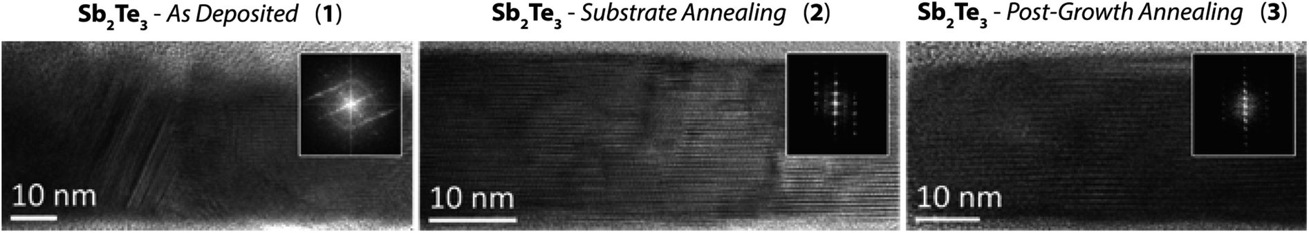 | ||
| Fig. 2 Cross sectional high resolution TEM images of the Sb2Te3 films: Sb2Te3 – As Deposited (1), Sb2Te3 – Substrate Annealing (2), and Sb2Te3 – Post-Growth Annealing (3). Insets: fast Fourier transform analyses. | ||
Amongst the three samples, Sb2Te3 – As Deposited (1) appeared to be the most granular and defective in nature (see also Fig. S9, ESI†). Its FFT also highlights the essentially random orientation of its grains, even though sometimes the c-axis was found to be almost perpendicular to the substrate. Consistently with the SEM and AFM data, the structure of Sb2Te3 – Substrate Annealing (2) revealed a much lower granularity and a more ordered growth. However, different crystallographic orientations were detected throughout the sample (Fig. S10, ESI†).
Lastly, Sb2Te3 – Post-Growth Annealing (3), in agreement with SEM and AFM results, appeared to be composed of larger building units (more details in Fig. S11, ESI†). The c-axis of the Sb2Te3 crystalline cell was almost always found to be perpendicular to the silicon substrate, while grains with very low misalignment were rarely observed. The van der Waals gaps of the Sb2Te3 quintuple layer structure are clearly visible and parallel to the substrate. The (003) periodicity along the c-axis, measured over many pictures, was 1 nm, consistently with the one calculated for the Sb2Te3 rhombohedral structure.
Regardless of the morphological and structural differences between the three films, their thickness, probed via XRR (see Fig. S23 and Table S1, ESI†), remained almost unchanged. In fact, films (2) and (3) showed thicknesses (32.5 and 32.0 nm, respectively) only slightly reduced respect to (1), fact that is principally explained by their higher crystallinity and enhanced packing.
Also, their composition, as determined from the ratio of the Sb and Te Lα lines detected by TXRF, was found consistent with the Sb2Te3 stoichiometry (Fig. S12 and S13, ESI†); similarly, XPS data of the various films (Fig. S14–S22, ESI†) are identical and consistent with literature values.36
XRD studies were undertaken to probe the Sb2Te3 films crystallinity and evaluate the relevance of the substrate annealing and post-growth processing on their structural properties. The Grazing Incidence X-ray Diffraction (GIXRD) pattern of 1 (Fig. 3a, black) exhibited intense reflections at 2θ = 8.46°, 17.3°, 26.0°, 28.26°, and ca. 38.4° corresponding to the 003, 006, 009, 015, and 1 0 10 reflections, attributed to the rhombohedral crystalline structure in the R![[3 with combining macron]](https://www.rsc.org/images/entities/char_0033_0304.gif) m space group.
m space group.
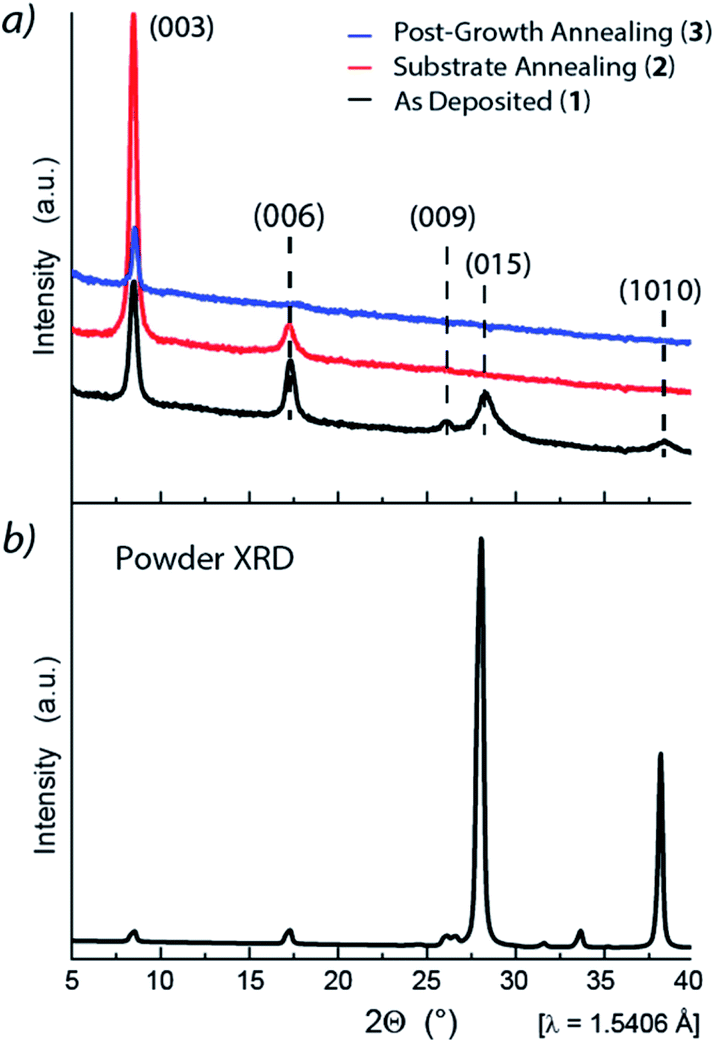 | ||
| Fig. 3 (a) Grazing incidence X-ray diffraction pattern of (bottom, black) Sb2Te3 – As Deposited, (red, middle) Sb2Te3 – Substrate Annealing, and (blue, top) Sb2Te3 – Post-Growth Annealing; (b) powder XRD pattern reference for Sb2Te3 measured at RT and atmospheric pressure. Lattice parameters: a = 4.264 Å and c = 30.458 Å (ICSD Inorganic Crystal Structure Database, FIZ Karlsruhe, 2019, file no. 2084).47 | ||
The relatively small linewidths of the (00![[small script l]](https://www.rsc.org/images/entities/char_e146.gif) ) peaks indicated high crystallinity while the (015) peak – the peak with the highest intensity in the powder diffractogram47 – indicated the polycrystalline nature of the film, and its broadening, possibly, a structural amorphous component.
) peaks indicated high crystallinity while the (015) peak – the peak with the highest intensity in the powder diffractogram47 – indicated the polycrystalline nature of the film, and its broadening, possibly, a structural amorphous component.
Interestingly, the 015 reflection was no longer observed in the Sb2Te3 – Substrate Annealing (2) thin film (Fig. 3a, red), whereas the 003 reflection was drastically enhanced, indicative of grains predominantly oriented along the [00] direction and, consequently, of a more crystalline structure. Moreover, the GIXRD of the Sb2Te3 – Post-Growth Annealing (3) film revealed an overall reduction of the peaks intensity (Fig. 3a, blue) suggesting substantial changes in the structure, compatible with a crystallinity improvement.
To assess the Sb2Te3 crystalline nature, XRD measurements were set up specifically to probe out-of-plane and in-plane orientations.
The XRD patterns collected in the Bragg–Brentano geometry (Fig. 4a) revealed the scattering of the reflections' intensity across ω (plot's y-axis), feature informative of the broadening in the (00) out-of-plane orientation.
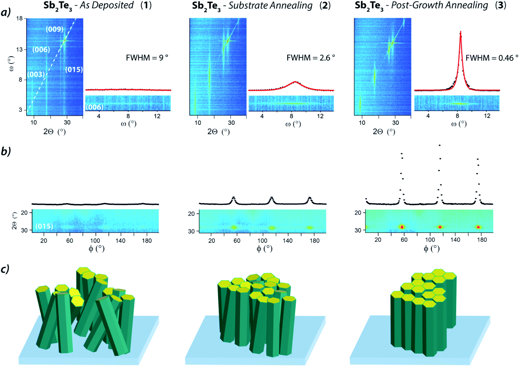 | ||
| Fig. 4 (a) XRD pattern collected in Bragg–Brentano geometry, including the profile of the (006) peak and the mosaicity values, and (b) φ angle scan of Sb2Te3 – As Deposited (1), Sb2Te3 – Substrate Annealing (2), and Sb2Te3 – Post-Growth Annealing (3). The dashed line in (a) evidences the Bragg–Brentano condition. The most intense signal in (a) is the 111 reflection pertaining to the silicon substrates and it is very close to the (015) peak. (c) Graphical representation of the Sb2Te3 crystalline ordering and orientation relative to the Si(111) substrate. | ||
While the full width at half maximum (FWHM) of the ω scan, (see plots in Fig. 4a) was substantial in 1 (up to 9°), it appeared much reduced in 2 (2.6°) and strongly contained in 3 that showed an FWHM value of 0.46°, indicating a mosaicity typical of epitaxial films and suggestive of single crystal-like materials.
These data, along with the absence of the 015 reflection (both in 2 and 3, consistently with the GIXRD – Fig. 3) indicated strongly (00) out-of-plane oriented grains in the Sb2Te3 – Post-Growth Annealing (3) film.
Moreover, the in-plane orientation, probed through a φ angle scan here optimized on the 015 reflection (2θ = 28.26°), appeared positively affected by Substrate Annealing and Post-Growth Annealing, too (Fig. 4b). In fact, while 1 showed almost no in-plane ordering, 60°-spaced peaks distinctive of the 3-fold symmetry of the Sb2Te3 rhombohedral cell (and related to the 015 reflection) emerged in the 2θ–φ plot of 2, as result of a preferential in-plane orientation (Fig. 4b). However, the faint line connecting the (015) peaks revealed residual disorder, indicative of a minor fraction of randomly oriented grains. Differently, the intense, precisely positioned, and narrow peaks of the 015 reflections observed in Sb2Te3 – Post-Growth Annealing (3) indicates an almost complete in-plane ordering (Fig. 4b). Combining the data from the Bragg–Brentano and the φ scan, the epitaxial relationship between the Sb2Te3 and the substrate is found as Sb2Te3[00]‖Si[111] and Sb2Te3[015]‖Si[011]. The latter epitaxial relationship was deduced by a careful positioning of the sample, in the way that the φ = 0 position corresponds to the Si[011] direction parallel to the X-ray beam (Fig. S24, ESI†).
The set of structural information attained from the microscopies and diffraction measurements can be rationalized as sketched in Fig. 4c. This visual representation highlights the structural and morphological transition from a highly granular and poorly oriented film (1) to a smoother and crystallographically out-of-plane ordered one (2), and, finally to an epitaxial layer, consisting of crystallites both in-plane and out-of-plane oriented (3).
The quality improvement observed comparing Sb2Te3 – As Deposited (1) and Sb2Te3 – Substrate Annealing (2) is the result of the Si(111) substrate annealing. A high temperature substrate treatment likely favors the removal of adventitious physisorbed or chemisorbed water, preventing from a disorderly initial-stage deposition, whereas we tend to exclude surface reconstruction phenomena that are known to take place at higher temperatures.48,49
In fact, as the MOCVD process was performed at room temperature, therefore not requiring the precursors' pyrolysis, residual surface water and hydroxyl groups would readily react with the protolyzable organometallic precursors, compromising the integrity of the silicon/Sb2Te3 interfacial van der Waals layers and possibly resulting in an uncontrolled deposition and an unordered and highly granular growth.
While some structural enhancement (out-of-plane orientation) was obtained upon substrate annealing, the most remarkable improvement was indeed achieved with the post-growth processing. This step is specifically responsible for the in-plane ordering. We speculate that the thermal treatment triggers a rearrangement of the grains into a thermodynamically preferred configuration allowed by the symmetry match between the substrate and the film. The crystallites preferential orientation is possibly induced by the surface-exposed crystalline lattice of Si(111). The working hypothesis for the selection of Si(111) as preferred substrate in the present study relies indeed on its surface lattice symmetry, analogous to the Sb2Te3 crystalline cell.
Conclusion
We grew antimony telluride continuous thin films by an MOCVD process unusually conducted at room temperature and described a successful approach to gain control over the structural quality of the films.Substrate annealing and post-growth annealing are found to effectively control the granularity, lower the roughness, and allow the growth of Sb2Te3 films on a highly lattice-mismatched substrate; nevertheless, the resulting thin films are highly oriented along the [00] direction, concomitantly with a specific in-plane crystalline order, a feature typical of an epitaxial growth.
This process appears therefore suitable for large scale preparation of epitaxial Sb2Te3 on Si(111), a substrate commonly adopted in microelectronics and for devices implementation.
Conflicts of interest
There are no conflicts to declare.Acknowledgements
We acknowledge the Horizon 2020 project SKYTOP “Skyrmion-Topological Insulator and Weyl Semimetal Technology” (FETPROACT-2018-01, no. 824123).Notes and references
- S. Manzeli, D. Ovchinnikov, D. Pasquier, O. V. Yazyev and A. Kis, Nat. Rev. Mater., 2017, 2, 17033 CrossRef CAS.
- M. Longo, O. Salicio, C. Wiemer, R. Fallica, A. Molle, M. Fanciulli, C. Giesen, B. Seitzinger, P. K. Baumann, M. Heuken and S. Rushworth, J. Cryst. Growth, 2008, 310, 5053–5057 CrossRef CAS.
- T. P. Ginley, Y. Wang and S. Law, Crystals, 2016, 6, 154 CrossRef.
- P. Guo, A. M. Sarangan and I. Agha, Appl. Sci., 2019, 9, 530 CrossRef CAS.
- M. Longo, T. Stoycheva, R. Fallica, C. Wiemer, L. Lazzarini and E. Rotunno, J. Cryst. Growth, 2013, 370, 323–327 CrossRef CAS.
- E. Rotunno, M. Longo, C. Wiemer, R. Fallica, D. Campi, M. Bernasconi, A. R. Lupini, S. J. Pennycook and L. Lazzarini, Chem. Mater., 2015, 27, 4368–4373 CrossRef CAS.
- S. Selmo, S. Cecchi, R. Cecchini, C. Wiemer, M. Fanciulli, E. Rotunno, L. Lazzarini and M. Longo, Phys. Status Solidi A, 2016, 213, 335–338 CrossRef CAS.
- N. Zibouche, A. Kuc, J. Musfeldt and T. Heine, Ann. Phys., 2014, 526, 395–401 CrossRef CAS.
- J. E. Boschker and R. Calarco, Adv. Phys.: X, 2017, 2, 675–694 CAS.
- D. Campi, L. Paulatto, G. Fugallo, F. Mauri and M. Bernasconi, Phys. Rev. B, 2017, 95, 024311 CrossRef.
- R. Venkatasubramanian, E. Siivola, T. Colpitts and B. O'Quinn, Nature, 2001, 413, 597–602 CrossRef CAS PubMed.
- S. Zastrow, J. Gooth, T. Boehnert, S. Heiderich, W. Toellner, S. Heimann, S. Schulz and K. Nielsch, Semicond. Sci. Technol., 2013, 28, 035010 CrossRef.
- Y. V. Ivanov, A. T. Burkov and D. A. Pshenay-Severin, Phys. Status Solidi B, 2018, 255, 1800020 CrossRef.
- H. Zhang, C.-X. Liu, X.-L. Qi, X. Dai, Z. Fang and S.-C. Zhang, Nat. Phys., 2009, 5, 438–442 Search PubMed.
- J. J. Cha, K. J. Koski and Y. Cui, Phys. Status Solidi RRL, 2013, 7, 15–25 Search PubMed.
- G.-H. Dong, Y.-J. Zhu and L.-D. Chen, CrystEngComm, 2011, 13, 6811–6816 RSC.
- Y. Saito, P. Fons, A. V. Kolobov and J. Tominaga, Phys. Status Solidi B, 2015, 252, 2151–2158 CrossRef CAS.
- Y. Saito, P. Fons, L. Bolotov, N. Miyata, A. V. Kolobov and J. Tominaga, AIP Adv., 2016, 6, 045220 CrossRef.
- P. Marchand, I. A. Hassan, I. P. Parkin and C. J. Carmalt, Dalton Trans., 2013, 42, 9406–9422 RSC.
- S. L. Benjamin, C. H. de Groot, A. L. Hector, R. Huang, E. Koukharenko, W. Levason and G. Reid, J. Mater. Chem. C, 2015, 3, 423–430 RSC.
- V. Pore, T. Hatanpää, M. Ritala and M. Leskelä, J. Am. Chem. Soc., 2009, 131, 3478–3480 CrossRef CAS PubMed.
- K. Knapas, T. Hatanpää, M. Ritala and M. Leskelä, Chem. Mater., 2010, 22, 1386–1391 CrossRef CAS.
- D. Nminibapiel, K. Zhang, M. Tangirala, H. Baumgart, V. S. K. Chakravadhanula, C. Kübel and V. Kochergin, ECS J. Solid State Sci. Technol., 2014, 3, P95–P100 CrossRef CAS.
- V. Pore, K. Knapas, T. Hatanpää, T. Sarnet, M. Kemell, M. Ritala, M. Leskelä and K. Mizohata, Chem. Mater., 2011, 23, 247–254 CrossRef CAS.
- T. Eom, T. Gwon, S. Yoo, B. J. Choi, M.-S. Kim, S. Ivanov, A. Adamczyk, I. Buchanan, M. Xiao and C. S. Hwang, J. Mater. Chem. C, 2015, 3, 1365–1370 RSC.
- L. Zheng, X. Cheng, D. Cao, Q. Wang, Z. Wang, C. Xia, L. Shen, Y. Yu and D. Shen, RSC Adv., 2015, 5, 40007–40011 RSC.
- G. Wang, X. Zhu, J. Wen, X. Chen, K. He, L. Wang, X. Ma, Y. Liu, X. Dai, Z. Fang, J. Jia and Q. Xue, Nano Res., 2010, 3, 874–880 CrossRef CAS.
- N. Peranio, M. Winkler, D. Bessas, Z. Aabdin, J. König, H. Böttner, R. P. Hermann and O. Eibl, J. Alloys Compd., 2012, 521, 163–173 CrossRef CAS.
- J. Kampmeier, C. Weyrich, M. Lanius, M. Schall, E. Neumann, G. Mussler, T. Schäpers and D. Grützmacher, J. Cryst. Growth, 2016, 443, 38–42 CrossRef CAS.
- F. Bonell, M. G. Cuxart, K. Song, R. Robles, P. Ordejón, S. Roche, A. Mugarza and S. O. Valenzuela, Cryst. Growth Des., 2017, 17, 4655–4660 CrossRef CAS.
- R. Venkatasubramanian, T. Colpitts, B. O'Quinn, S. Liu, N. El-Masry and M. Lamvik, Appl. Phys. Lett., 1999, 75, 1104–1106 CrossRef CAS.
- A. Giani, A. Boulouz, F. Pascal-Delannoy, A. Foucaran, E. Charles and A. Boyer, Mater. Sci. Eng., B, 1999, 64, 19–24 CrossRef.
- G. Bendt, S. Schulz, S. Zastrow and K. Nielsch, Chem. Vap. Deposition, 2013, 19, 235–241 CrossRef CAS.
- G. Bendt, S. Zastrow, K. Nielsch, P. S. Mandal, J. Sánchez-Barriga, O. Rader and S. Schulz, J. Mater. Chem. A, 2014, 2, 8215–8222 RSC.
- P. I. Kuznetsov, B. S. Shchamkhalova, V. O. Yapaskurt, V. D. Shcherbakov, V. A. Luzanov, G. G. Yakushcheva, V. A. Jitov and V. E. Sizov, J. Cryst. Growth, 2017, 471, 1–7 CrossRef CAS.
- A. A. Volykhov, J. Sánchez-Barriga, A. P. Sirotina, V. S. Neudachina, A. S. Frolov, E. A. Gerber, E. Y. Kataev, B. Senkovsky, N. O. Khmelevsky, A. Y. Aksenenko, N. V. Korobova, A. Knop-Gericke, O. Rader and L. V. Yashina, Chem. Mater., 2016, 28, 8916–8923 CrossRef CAS.
- R. Cecchini, R. Mantovan, C. Wiemer, L. Nasi, L. Lazzarini and M. Longo, Phys. Status Solidi RRL, 2018, 12, 1800155 CrossRef.
- E. Longo, C. Wiemer, R. Cecchini, M. Longo, A. Lamperti, A. Khanas, A. Zenkevich, M. Fanciulli and R. Mantovan, J. Magn. Magn. Mater., 2019, 474, 632–636 CrossRef CAS.
- E. Longo, R. Mantovan, R. Cecchini, M. D. Overbeek, M. Longo, G. Trevisi, L. Lazzarini, G. Tallarida, M. Fanciulli, C. H. Winter and C. Wiemer, Nano Res., 2020, 13, 570–575 CrossRef CAS.
- R. D. Dupuis, J. Cryst. Growth, 1997, 178, 56–73 CrossRef CAS.
- T. Detchprohm, J.-H. Ryou, X. Li and R. D. Dupuis, in Metalorganic Vapor Phase Epitaxy (MOVPE), ed. S. Irvine and P. Capper, Wiley, Haboken, NJ, 2020, ch. 14, pp. 507–548 Search PubMed.
- G. Bendt, K. Kaiser, A. Heckel, F. Rieger, D. Oing, A. Lorke, N. P. Rodriguez, G. Schierning, C. Jooss and S. Schulz, Semicond. Sci. Technol., 2018, 33, 105002 CrossRef.
- F. Rieger, V. Roddatis, K. Kaiser, G. Bendt, S. Schulz and C. Jooss, Phys. Rev. Mater., 2020, 4, 025402 CrossRef CAS.
- G. Bendt, J. Sonntag, A. Lorke, W. Assenmacher, U. Hagemann and S. Schulz, Semicond. Sci. Technol., 2015, 30, 085021 CrossRef.
- T. J. Groshens, R. W. Gedridge Jr and C. K. Lowe-Ma, Chem. Mater., 1994, 6, 727–729 CrossRef CAS.
- T. J. Groshens, R. W. Gedridge, R. Scheri and T. Cole, in Fifteenth International Conference on Thermoelectrics. Proceedings ICT '96, 1996, pp. 430–434 Search PubMed.
- FIZ Karlsruhe, ICSD Inorganic Crystal Structure Database, 2019, file no. 2084.
- R. J. Phaneuf, E. D. Williams and N. C. Bartelt, Phys. Rev. B: Condens. Matter Mater. Phys., 1988, 38, 1984–1993 CrossRef CAS PubMed.
- Y.-L. Wang, H.-M. Guo, Z.-H. Qin, H.-F. Ma and H.-J. Gao, J. Nanomater., 2008, 2008, 874213 Search PubMed.
Footnote |
| † Electronic supplementary information (ESI) available: Additional SEM, AFM, and TEM images and characterization data. See DOI: 10.1039/d0ra02567d |
| This journal is © The Royal Society of Chemistry 2020 |