
 Open Access Article
 This Open Access Article is licensed under a Creative Commons Attribution-Non Commercial 3.0 Unported Licence
Atomic and electronic structure of solids of Ge2Br2PN, Ge2I2PN, Sn2Cl2PN, Sn2Br2PN and Sn2I2PN inorganic double helices: a first principles study
T. K. Bijoy†
 ab,
P. Muruganb and
Vijay Kumar*ac
ab,
P. Muruganb and
Vijay Kumar*ac
aDr Vijay Kumar Foundation, 1969 Sector 4, Gurgaon 122001, Haryana, India. E-mail: vijay.kumar@snu.edu.in
bCSIR-Central Electrochemical Research Institute, Karaikudi 630003, Tamil Nadu, India
cCenter for Informatics, School of Natural Sciences, Shiv Nadar University, NH-91, Tehsil Dadri, Gautam Buddha Nagar 201314, Uttar Pradesh, India
First published on 14th April 2020
Abstract
We report the results of density functional theory calculations on the atomic and electronic structure of solids formed by assembling A2B2PN (A = Ge and Sn, B = Cl, Br, and I) inorganic double helices. The calculations have been performed using a generalized gradient approximation for the exchange–correlation functional and including van der Waals interactions. Our results show that the double helices crystallize in a monoclinic lattice with van der Waals type weak interactions between the double helices. In all cases except Ge2Cl2PN, the solids are stable with a binding energy between the double helices ranging from 0.06 eV per atom to 0.09 eV per atom and inter-double helices separation of more than 3.33 Å. All the solids are semiconducting. Further calculations have been done by using meta-GGA with a modified Becke–Johnson functional to obtain better band gaps, which are found to lie in the range of 0.91 eV to 1.49 eV. In the case of Ge2Br2PN the solid is a direct band gap semiconductor although the isolated double helix has an indirect band gap and it is suggested to be interesting for photovoltaic, and other optoelectronic applications. The charge transfer between the atoms has been studied using Bader charge analysis and the DDEC6 method in the CHARGEMOL program, which suggests charge transfer from the outer helix to the inner helix.
Introduction
Double helical structures are very common in biological systems and it was believed that only carbon containing compounds can form this interesting geometry. But, in the past few decades inorganic double helices with structural similarity to DNA1 have been the subject of much interest in the search for non-carbon based such structures and they have been found in many cases.2–9 While progress in this direction is slow, an interesting development has been the finding10 of a double helix structure of a simple binary system LiP. Many other systems in this family of group I and group V elements have also been studied, and it was revealed that the structural and vibrational properties are sensitive to the constituent elements.11 In these systems charge transfer from an alkali metal to group V element would tend to make the latter behave like the next element such as P to behave like S in the case of LiP. It is to be noted that a double helical structure of selenium, an element just below S in the periodic table, has been reported12 to occur in a double wall carbon nanotube. Also, sulphur favours polymeric chains13 and a one-dimensional helical structure of phosphorous has also been reported.14,15 Some of the earlier reported inorganic double helices, such as, [(CH3)2NH2]K4[V10O10(H2O)2(OH)4(PO4)7]·4H2O and the combination of cadmium sulphide and cadmium tellurium forms very complicated double helical geometry.16,17 Yet another interesting recent development has been the finding of carbon free inorganic double helices of a relatively simple system, SnIP and their needle-like solids.18–20 Both theoretical and experimental studies suggest that these inorganic double helices crystallize in monoclinic structure. The SnIP double helix has two interpenetrating helices: (i) outer SnI helix and (ii) inner P helix. In the solid phase the unit cell has two SnIP double helices separated by 3.70 Å and they interact with each other via weak van der Waals forces. Interestingly the electronic structure of SnIP double helix shows it to have a band gap of ≈1.86 eV, which is suitable for absorbing visible light. Hence this semiconducting material is interesting as a catalyst for photocatalytic water splitting reaction,21 photovoltaic, optoelectronic, and photoconducting22 applications. Also, such structures are interesting for flexible electronics, as well as atomic scale mechanical and sensor applications. Nilges and co-workers have recently reported that the SnIP double helices are capable of forming heterostructure with g-C3N4 and this heterostructure shows remarkable photocatalytic water splitting.23 These developments are naturally very interesting as they open up new possibilities of materials design and also there is the question of the usefulness of such materials in biological systems. Following the discovery of SnIP inorganic double helices, recently a theoretical study has predicted other double helices of ABP type in the same group, where A = Si–Pb and B = Cl–I.24 Similar to SnIP solid, these systems also stabilize in the same crystal structure.Inspired from these recent developments, in an earlier study we have reported the atomic structure and electronic properties of inorganic double helices of the type A2B2XY. Here A = Si–Pb and B = Cl–I, and therefore the outer helix is similar to the case of SnIP but the inner P helix is a heteroatomic XY (XY = PN and SiS) helix.25 These choices were motivated from the fact that PN also forms polymeric chain structures and SiS satisfies the valency requirement besides the fact that S is also good from the point of view of forming polymeric structures. It was shown that the heteroatomic inner helix not only expends the family of double helical structures, but also the double helices with a PN inner helix were found to be even more stable than those with a pure P helix. Such heteroatomic helices can also provide flexibility to optimize the atomic and the electronic structure. Further, this study shed light on the factors that may lead to the formation of inorganic double helices. Similar to the parent SnIP type inorganic double helices, these new double helices also show semiconducting behavior with a sizeable band gap. Moreover, by adding impurities to the double helix, p type double helices were shown for the first time to be favorable.25 However, it is also important to know if these double helices could exist in a solid form and are stable as in experiments bundles or crystals of double helices are likely to be found as for SnIP. Keeping this in mind, in this work we have studied assemblies of A2B2XY inorganic double helices in the form of their solid structures. Here we report our results on solids of five inorganic double helices, namely Ge2Br2PN, Ge2I2PN, Sn2Cl2PN, Sn2Br2PN, and Sn2I2PN which have been found to be stable. It is noteworthy to mention that we also attempted to assemble double helices of other combination from this group such as Si2I2PN and Ge2Cl2PN, but they were found to be structurally unstable. Our results show that all the double helices reported here form a solid phase in a monoclinic structure with the helices separated from each other by 3.34 Å or more, suggesting that they are weakly interacting with each other as also in the case of SnIP. Hence our work also suggests the possibility to exfoliate the individual nanowire from their respective bulk phase. Moreover, this will open up a new avenue to make heterostructures using these novel nanostructures for potential applications.
Computational methodology
The calculations have been performed using Vienna Ab initio Simulation Package (VASP) within the framework of van der Waals corrected density functional theory.26,27 We used projector augmented wave (PAW) pseudopotential method28 to describe electron–ion interactions while the exchange–correlation functional has been treated within generalized gradient approximation (GGA) of Perdew, Burke, and Ernzerhof (PBE).29 The Brillouin zone integrations for the optimization of the atomic structure of the solid have been performed using Monkhorst–Pack 4 × 6 × 2 k-points mesh. For incorporating van der Waals correction, we performed calculations in all the cases using Grimme's DFT-D2 method.30 The structure optimization calculations were performed without considering any symmetry and allowing ionic positions, cell shape, and volume to relax. The iterative relaxation process was repeated until the absolute value of force on each ion was converged to less than 0.005 eV Å−1. The convergence for energy was set to be 10−5 eV. Further, we have calculated the bandgap using the meta-GGA with modified Becke–Johnson (mBJ) functional31 that yields band gaps with accuracy similar to GW method.Results and discussion
To begin with, we modelled the atomic structure of the solids of A2B2PN (A = Ge and Sn, B = Cl, Br, and I) double helices in a way similar to that of SnIP bulk structure. Fig. 1 shows the optimized atomic structures of the solids in five cases which are found to be stable. Similar to the case of SnIP solid, the unit cell of these solids contains two double helices with one right-handed double helix and the other, left-handed double helix. Each double helix contains 42 atoms and therefore the solid form of A2B2PN double helix has 84 atoms in the unit cell. All these solids are non-magnetic and semiconducting. Similar to the isolated double helices, in the bulk phase also the double helices are chemically bonded along the axis of the helix while along the other two directions the double helices are weakly interacting. The various structural features of the completely relaxed structures are given in Table 1. Our results show that the lattice parameters along all the three directions increase when we move from Ge to Sn and Cl to I. This is due to the increase in the bond lengths in the outer A–B helix. In the case of Ge2Br2PN and Ge2I2PN solids, the mean nearest neighbour bond lengths in the outer helix are 2.79 Å and 2.99 Å, respectively. In the same way the A–B bond lengths in Sn2Cl2PN, Sn2Br2PN, and Sn2I2PN are 2.80 Å, 2.94 Å, and 3.11 Å, respectively. It is interesting to note that the P–N bond length in the inner helix remains almost constant (∼1.77 Å) in all the cases. Further to calculate the distance between the double helices in the bulk structure, we measured the inter double helices A–B (dA′–B′) and B–B (dB′–B′) distances. The obtained results are given in Table 1. The shortest inter-double helices distance 3.34 Å is obtained for Sn2Cl2PN solid. In all other cases, the double helices are separated by more than 3.34 Å, suggesting that they are weakly interacting through van der Waals force of attraction.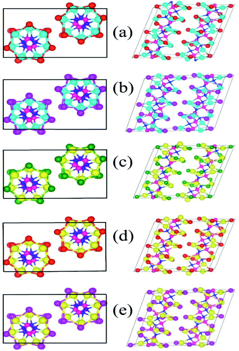 | ||
| Fig. 1 The optimized atomic structures of solids of (a) Ge2Br2PN, (b) Ge2I2PN, (c) Sn2Cl2PN, (d) Sn2Br2PN, and (e) Sn2I2PN double helices. The top (side) view of each system is shown in the left (right) panel. Cyan, yellow, green, magenta, red, blue, and pink balls represent Ge, Sn, Cl, Br, I, P, N, Cl, N, and P atoms, respectively. | ||
| Double helix | a (Å) | b (Å) | c (Å) | dA–B (Å) | dP–N (Å) | dA′–B′ (Å) | dB′–B′ (Å) | Eb (eV per atom) | Eg (eV) |
|---|---|---|---|---|---|---|---|---|---|
| Ge2Br2PN | 13.94 | 8.88 | 16.61 | 2.79 | 1.77 | 3.51 | 3.40 | 0.070 | 1.49 (1.13) |
| Ge2I2PN | 14.00 | 9.43 | 17.30 | 2.99 | 1.77 | 3.68 | 3.56 | 0.064 | 1.41 (1.04) |
| Sn2Cl2PN | 14.42 | 8.65 | 16.66 | 2.80 | 1.76 | 3.34 | 3.40 | 0.093 | 1.04 (0.71) |
| Sn2Br2PN | 14.45 | 9.08 | 17.18 | 2.94 | 1.76 | 3.51 | 3.45 | 0.091 | 0.94 (0.66) |
| Sn2I2PN | 14.51 | 9.63 | 17.82 | 3.11 | 1.77 | 3.66 | 3.57 | 0.075 | 0.91 (0.64) |
A similar behaviour was earlier obtained in the case of the solid of SnIP double helices. Next, we calculated the binding energy/atom (Eb) to understand the strength of interaction between the double helices in the solid phase, from
Here E(A2B2PN)single and E(A2B2PN)solid represent the dispersion corrected total energies of one A2B2PN double helix and the solid form, respectively, while N is the total number of atoms in the unit cell. Among the aforesaid double helices, the maximum value of Eb (0.093 eV per atom) is obtained for Sn2Cl2PN while the lowest value (0.064 eV per atom) is obtained for Ge2I2PN. In general, the variation in Eb suggests that the interaction between the double helices increases as we move from I to Cl. Also, the binding energy of Sn2B2PN is higher than the value for Ge2B2PN for B = Br and I. In order to further understand the energetic stability of these double helices, we also calculated the cohesive energy (Ec) using the following equation
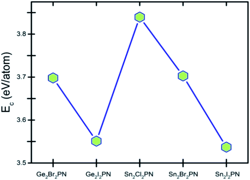
Here, E(A), E(B), E(P), and E(N) denote the atomic energies of the constituent atoms present in the double helix. E(A2B2PN)solid refers to the total energy of the A2B2PN bulk while n represents the number of formula units in the unit cell of the solid. The calculated Ec values are plotted in Fig. 2 and the results show that the Sn2Cl2PN solid has the highest Ec value (3.84 eV per atom) among the five solids of double helices we have studied, while the values for Ge2Br2PN and Sn2Br2PN solids are 3.69 eV per atom and 3.70 eV per atom, respectively. Similarly, the Ge2I2PN and Sn2I2PN solid have nearly the same values (3.55 and 3.54 eV per atom, respectively). It should be noted that Ec gradually decreases as we move from Cl to I. Since all these double helices are heteroatomic systems, we further studied the charge transfer between the constituent atoms by performing Bader charge (QB) analysis32,33 using all electron charge density and the results are given in Table 2. The Bader charge analysis shows that each Ge atom in the outer helix of Ge2Br2PN donates nearly 0.88e while the Br atoms in the same helix receive only 0.51e. Thus, it is clear that the remaining charge is transferred to the inner helix.
 | ||
| Fig. 2 Cohesive energy (Ec) of solids of A2B2PN double helices. Points are connected to aid eyes to see the trend. | ||
| Double helices | QB(A) e | QB(B) e | QB(N) e | QB(P) e |
|---|---|---|---|---|
| Ge2Br2PN | +0.88 (+0.42) | −0.51 (−0.32) | −1.66 (−0.45) | +0.93 (+0.24) |
| Ge2I2PN | +0.77 (+0.33) | −0.39 (−0.23) | −1.66 (−0.43) | +0.91 (+0.24) |
| Sn2Cl2PN | +1.07 (+0.55) | −0.67 (−0.42) | −1.71 (−0.48) | +0.92 (+0.20) |
| Sn2Br2PN | +0.98 (+0.51) | −0.59 (−0.36) | −1.70 (−0.19) | +0.92 (+0.47) |
| Sn2I2PN | +0.91 (+0.42) | −0.49 (−0.28) | −1.70 (−0.47) | +0.88 (+0.19) |
Further, the electronegativities of P and N atoms are different, and similar to the outer helix, in the inner helix also we find charge transfer from less electronegative P to more electronegative N. The charge transfer in the outer helix reduces when I atom replaces Br. It is worth to mention that the charge transfer is enhanced when we move from Ge to Sn. This is due to the more extended nature of valence orbitals of Sn. As a result, the outer helix becomes more ionic. Our Bader charge analysis is consistent with the previous study25 on A2B2PN double helices. Further, we analysed the charge transfer in the above said systems by using DDEC6 CHARGEMOL code.34,35 Although, we find significant variation in the charge state of each atom, namely less charge transfer compared with the Bader charge analysis, the overall charge transfer trend is found to be the same.
Fig. 3 shows the total and the site as well as angular momentum decomposed partial densities of states of various A2B2PN double helices calculated using GGA-PBE exchange–correlation functionals. The results show that all the solids of the double helices are semiconducting with the band gap of 1.13 eV, 1.04 eV, 0.71 eV, 0.66 eV, and 0.64 eV, respectively, for Ge2Br2PN, Ge2I2PN, Sn2Cl2PN, Sn2Br2PN, and Sn2I2PN. A similar trend in the value of the band gap was found in the case of A2B2PN double helices in our previous study.25 Here, all the above said bandgap values have been obtained using PBE calculation including the dispersion correction as discussed in the computational methodology section. As GGA (PBE) generally underestimates the band gap, we expect the actual values to be higher. Fig. 3 also shows that the valence band maximum (VBM) of Ge2Br2PN as well as Ge2I2PN mainly arises from 4p and 5p orbitals of the respective halogen atoms in the outer helix. On the other hand, the conduction band minimum (CBM) has dominant contribution from the 4p bands of Ge atoms.
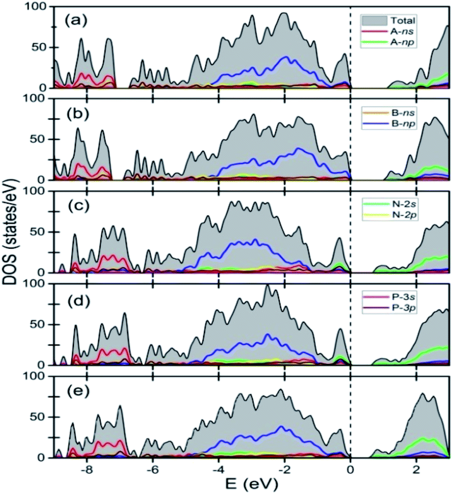 | ||
| Fig. 3 Site and angular momentum resolved electronic density of states of A2B2PN solids: (a) Ge2Br2PN, (b) Ge2I2PN, (c) Sn2Cl2PN, (d) Sn2Br2PN, and (e) Sn2I2PN. The top of the valence band has been taken as reference for energy. | ||
However, in the case of Sn2Cl2PN and Sn2Br2PN, the states near the VBM predominantly arise from the 5p states of Sn atoms, as the bands coming from the halogen atoms in the valence band region lie lower in energy. But, similar to the Ge based double helices, here also the states near the CBM are mainly contributed by the valence 5p bands of Sn atoms.
Next, to get further insight on the semiconducting nature of these solids of double helices and to obtain more reliable values for the band gap, we calculated the electronic band structure using the mBJ method. Our results show that there is an increase in the value of the band gap when we use mBJ method on comparing the GGA values. In Fig. 4 we have shown the results for all the stable A2B2PN double helices. The band gap values are 1.49, 1.41, 1.04, 0.94, and 0.91 eV, respectively, for Ge2Br2PN, Ge2I2PN, Sn2Cl2PN, Sn2Br2PN, and Sn2I2PN. It can be seen that in all the cases, the VBM and CBM are located on the Γ point. However, it is also noted that in most of the cases, the VBM exist in multiple points. Therefore, these systems are quasi-direct bandgap semiconductor. It is noteworthy that there is a transition from indirect to direct band gap nature for Ge2Br2PN, when we assemble the isolated Ge2Br2PN double helix to form its bulk phase. Therefore, it is concluded that the weak van der Waals interactions between the double helices in the solid change this indirect gap into a direct/quasi direct band gap. The obtained mBJ bandgap of the Ge2Br2PN solid is 1.49 eV which is excellent for photovoltaic applications as also in the case of currently well studied organo-metallic perovskite materials.36 Hence this would make these solids very interesting for optoelectronic and photovoltaic applications.
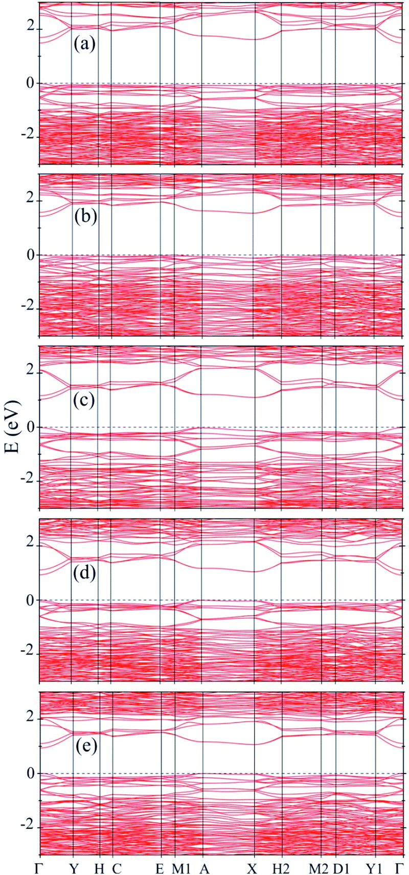 | ||
| Fig. 4 Electronic band structure of solids of (a) Ge2Br2PN, (b) Ge2I2PN, (c) Sn2Cl2PN, (d) Sn2Br2PN, and (e) Sn2I2PN inorganic double helices calculated using DFT-mBJ method. The top of the valence band has been taken as reference for energy. | ||
Conclusions
In brief, we have performed dispersion-corrected DFT calculations to explore the atomic and electronic structure of solids of A2B2PN (A = Ge and Sn, B = Cl, Br, and I) inorganic double helices. Our results suggest that in many cases the A2B2PN double helices can be assembled to form a stable monoclinic crystal. The interaction between the adjacent double helices in the solid phase is weak van der Waals force of attraction and in all the five double helices that we found to form stable solids; the inter-double helix distance is more than 3.33 Å. The Bader charge as well as DDEC6 analysis of the A2B2PN double helices shows that there occurs significant charge transfer from the tetravalent atom ‘A’ to both B atoms of the outer helix as well as to N atoms of the inner PN helix. Also, in contrast to SnIP double helices, there is polar character in the inner helix due to charge transfer from P to N atoms. The charge transfer from the outer helix to the inner helix also helps to stabilize the double helical structure. Interestingly, the electronic structure shows that all the solids of the double helices are semiconductors with the band gap ranging from 0.91 eV to 1.49 eV. Since the mBJ method is good for producing the experimentally reported band gap, we believe that these values would be close to their actual band gap. Our results suggest that Ge based solids of these inorganic double helices may be particularly interesting for many applications including photovoltaic, optoelectronic, and other nano-electronic flexible devices, since their bandgap falls in the range ideal for the above said applications. The formation of solid structure suggests that these types of solid phases can be synthesized. Hence, we believe that our work will motivate experimentalists to realize these systems in laboratory.Conflicts of interest
There are no conflicts of interest to declare.Acknowledgements
T. K. B. expresses deep gratitude for the hospitality at the Dr Vijay Kumar Foundation. Partial support from International Technology Center–Pacific is gratefully acknowledged. We also thankfully acknowledge the use of the high-performance computing facility Magus of Shiv Nadar University and CSIR-CECRI.Notes and references
- J. D. Watson and F. H. C. Crick, Nature, 1953, 171, 737–738 CrossRef CAS PubMed.
- J.-M. Lehn, A. Rigault, J. Siegel, J. Harrowfield, B. Chevrier and D. Moras, Proc. Natl. Acad. Sci. U. S. A., 1987, 84, 2565–2569 CrossRef CAS PubMed.
- E. C. Constable, M. D. Ward, M. G. B. Drew and G. A. Forsyth, Polyhedron, 1989, 8, 2551–2555 CrossRef CAS.
- P. K.-K. Ho, S.-M. Peng, K.-Y. Wong and C.-M. Che, J. Chem. Soc., Dalton Trans., 1996, 1829–1834 RSC.
- V. Soghomonian, Q. Chen, R. C. Haushalter, J. Zubieta and C. J. O'Connor, Science, 1993, 259, 1596–1599 CrossRef CAS PubMed.
- M. T. Caudle, R. A. Nieman and V. G. Young, Inorg. Chem., 2001, 40, 1571–1575 CrossRef CAS PubMed.
- C. Gieck, V. Derstroff, T. Block, C. Felser, G. Regelsky, O. Jepsen, V. Ksenofontov, P. Gütlich, H. Eckert and W. Tremel, Chem.–Eur. J., 2004, 10, 382–391 CrossRef CAS PubMed.
- Y. Koyama, Y. Hayashi and K. Isobe, Chem. Lett., 2008, 37, 578–579 CrossRef CAS.
- D. S. Su, Angew. Chem., Int. Ed., 2011, 50, 4747–4750 CrossRef CAS PubMed.
- A. S. Ivanov, A. J. Morris, K. V. Bozhenko, C. J. Pickard and A. I. Boldyrev, Angew. Chem., Int. Ed., 2012, 51, 8330–8333 CrossRef CAS PubMed.
- W. Ju, H. Wang, T. Li, H. Liu and H. Han, RSC Adv., 2016, 6, 50444–50450 RSC.
- T. Fujimori, R. B. dos Santos, T. Hayashi, M. Endo, K. Kaneko and D. Tománek, ACS Nano, 2013, 7, 5607–5613 CrossRef CAS PubMed.
- H. Mutlu, E. B. Ceper, X. Li, J. Yang, W. Dong, M. M. Ozmen and p. Theato, Macromol. Rapid Commun., 2019, 40, 1800650 CrossRef PubMed.
- D. Liu, J. Guan, J. Jiang and D. Tomanek, Nano Lett., 2016, 16, 7865–7869 CrossRef CAS PubMed.
- G. Sansone, L. Maschio and A. J. Karttunen, Chem.–Eur. J., 2017, 23, 15884–15888 CrossRef CAS PubMed.
- V. Soghomonian, Q. Chen, R. C. Haushalter, J. Zubieta and C. J. O'Conner, Science, 1993, 259, 1596–1599 CrossRef CAS PubMed.
- S. Srivastava, et al., Light-controlled self-assembly of semiconductor nanoparticles into twisted ribbons, Science, 2010, 327, 1177218 CrossRef PubMed.
- D. Pfister, K. Schäfer, C. Ott, B. Gerke, R. Pöttgen, O. Janka, M. Baumgartner, A. Efimova, A. Hohmann, P. Schmidt, S. Venkatachalam, L. van Wüllen, U. Schürmann, L. Kienle, V. Duppel, E. Parzinger, B. Miller, J. Becker, A. Holleitner, R. Weihrich and T. Nilges, Adv. Mater., 2016, 28, 9783–9791 CrossRef CAS PubMed.
- L. M. A. Saleh, R. Dziedzic and A. M. Spokoyny, ACS Cent. Sci., 2016, 2, 685–686 CrossRef CAS PubMed.
- A. Utrap, N. Y. Xiang and T. Nilges, J. Cryst. Growth, 2017, 475, 341–345 CrossRef CAS.
- X. Li, Y. Dai, Y. Ma, M. Li, L. Yu and B. Huang, J. Mater. Chem. A, 2017, 5, 8484–8492 RSC.
- D. Purschke, E. Uzer, C. Ott, M. Pielmeier, N. Amer, T. Nilges and F. Hegmann, Canadian Association of Physicists Congress, 2019 Search PubMed.
- C. Ott, F. Reiter, M. Baumgartner, M. Pielmeier, A. Vogel, P. Walke, S. Burger, M. Ehrenreich, G. Kieslich, D. Daisenberger, J. Armstrong, U. K. Thakur, P. Kumar, S. Chen, D. Donadio, L. S. Walter, R. T. Weitz, K. Shankar and T. Nilges, Adv. Funct. Mater., 2019, 29, 1900233 CrossRef.
- M. Baumgartner, R. Weihrich and T. Nilges, Chem.–Eur. J., 2017, 23, 6452–6457 CrossRef CAS PubMed.
- T. K. Bijoy, P. Murugan and V. Kumar, Phys. Chem. Chem. Phys., 2018, 20, 10060–10068 RSC.
- G. Kresse and D. Joubert, Phys. Rev. B: Condens. Matter Mater. Phys., 1999, 59, 1758–1775 CrossRef CAS.
- G. Kresse and J. Furthmuller, Phys. Rev. B: Condens. Matter Mater. Phys., 1986, 54, 11169–11186 CrossRef PubMed.
- P. E. Blochl, Phys. Rev. B: Condens. Matter Mater. Phys., 1994, 50, 17953–17979 CrossRef PubMed.
- J. P. Perdew, K. Burke and M. Ernzerhof, Phys. Rev. Lett., 1996, 77, 3865–3868 CrossRef CAS PubMed.
- S. Grimme, J. Comput. Chem., 2006, 27, 1787–1799 CrossRef CAS PubMed.
- A. D. Becke and E. R. Johnson, J. Chem. Phys., 2006, 124, 221101–221105 CrossRef PubMed.
- R. F. W. Bader, P. J. MacDougall and C. D. H. Lau, J. Am. Chem. Soc., 1984, 106, 1594–1605 CrossRef CAS.
- G. Henkelman, A. Arnaldsson and H. Jónsson, Comput. Mater. Sci., 2006, 36, 354–360 CrossRef.
- T. A. Manz, RSC Adv., 2017, 7, 45552–45581 RSC.
- T. A. Manz and N. Gabaldon Limas, RSC Adv., 2016, 6, 47771–47801 RSC.
- Z. Xiao, Y. Zhou, H. Hosono, T. Kamiya and N. P. Padture, Chem.–Eur. J., 2018, 24, 2305–2316 CrossRef CAS PubMed.
Footnote |
| † Present address: Indo-Korea Science and Technology Center, New Airport Road, Yelahanka, Bengaluru, 560065, India. |
| This journal is © The Royal Society of Chemistry 2020 |