
 Open Access Article
 This Open Access Article is licensed under a Creative Commons Attribution-Non Commercial 3.0 Unported Licence
Novel patterned sapphire substrates for enhancing the efficiency of GaN-based light-emitting diodes
Szu-Han Chao†
a,
Li-Hsien Yeh† b,
Rudder T. Wuc,
Kyoko Kawagishic and
Shih-Chieh Hsu*ad
b,
Rudder T. Wuc,
Kyoko Kawagishic and
Shih-Chieh Hsu*ad
aDepartment of Chemical and Materials Engineering, Tamkang University, New Taipei City, Taiwan. E-mail: roysos1@gmail.com
bDepartment of Chemical Engineering, National Taiwan University of Science and Technology, Taipei 10607, Taiwan
cSuperalloys and High Temperature Materials Group, National Institute for Materials Science, Tsukuba, Ibaraki, Japan
dWater Treatment Science and Technology Research Center, Tamkang University, New Taipei City, Taiwan
First published on 24th April 2020
Abstract
In this study, a novel patterned sapphire substrate (PSS) was used to obtain mesa-type light-emitting diodes (LED), which can efficiently reduce the threading dislocation densities. Silicon nitride (Si3N4) was used as a barrier to form the PSS, replacing the commonly used silicon dioxide (SiO2). The refractive index of Si3N4 is 2.02, which falls between those of sapphire (1.78) and GaN (2.4), so it can be used as a gradient refractive index (GRI) material, enhancing the light extraction efficiency (LEE) of light-emitting diodes. The simulation and experimental results obtained indicate that the LEE is enhanced compared with the conventional PSS-LED. After re-growing, we observed that an air void exists on the top of the textured Si3N4 layer due to GaN epitaxial lateral overgrowth (ELOG). Temperature-dependent PL was used to estimate the internal quantum efficiency (IQE) of the PSS-LED and that of the PSS-LED with the Si3N4 embedded air void (PSA-LED). The IQE of the PSA-LED is 4.56 times higher than that of the PSS-LED. Then, a TracePro optical simulation was used to prove that the air voids will affect the final luminous efficiency. The luminous efficiency of the four different structures considered is ranked as Si3N4 (PSN-LED) > PSA-LED > PSS-LED with SiO2 (PSO-LED) > PSS-LED. Finally, we fabricated LED devices with different thickness of the Si3N4 barrier. The device shows the best luminance–current–voltage (LIV) performance when the Si3N4 thickness is 220 nm.
1. Introduction
Recently, nitride-based LEDs play an important role in solid-state lighting due to their advantages of high efficiency, long life, small size, and environmental protection. They have been widely used in various applications, such as traffic signals, full color displays, and back lights in liquid crystal displays.1–3 Although GaN-based LEDs with high brightness are commercially available, the light output power of these LEDs is still limited by low internal quantum efficiency and light extraction efficiency.4–7 Generally, a conventional GaN-based LED is grown on sapphire substrates in spite of the fact that the two have a lattice and coefficient of thermal expansion mismatch of 16% and 34%, respectively. These results in the GaN film producing a dislocation density in the order of 109 to 1011 cm−2.8,9 Thus, many techniques have been developed to improve GaN-based LEDs' IQE and LEE, such as using epitaxial lateral overgrowth,10–12 surface roughing,13–16 microstructured air cavities,17 isoelectronic doping,18 patterned sapphire with a silica array,19 metal mirror reflection layers,20–23 and patterned sapphire substrates.24–29The PSS is commonly used to reduce the threading dislocations and enhance IQE.30 When light penetrates from GaN into the air, the refractive index of GaN (n = 2.4) causes a critical angle of only 23.6 degrees and make most of the light reflect to the inner part of the device due to total internal reflection (TIR). As the light gets absorbed by the active layer, LEE degrades.31,32 In order to solve this problem, PSS is proven that is a useful technique, which can damage the flat interface. It would destroy the TIR effect at the emitting interface, so, more light can be extracted out to the outer ambient. Hence, it can significantly increase the light output of LED.33,34 This technique utilizes the patterns created on the sapphire wafers. The patterned SiO2 barrier35 is coated first on sapphire substrate and then form the mesa structure by the following dry etching process. Finally, GaN LED epitaxial structure36,37 are grown on the PSS wafers with this kind of mesa patterns. In the case of this fabrication process, SiO2 barrier is not totally etched and still retain between the PSS and GaN. The light emits from GaN epilayer and pass through the SiO2 thin film layer to sapphire substrate.38,39 The light path is affected by the different refractive index of materials.40 The refractive index of SiO2 is 1.55 and this value is lower than that of sapphire (n = 1.78) and GaN (n = 2.4).41 The difference of refractive index between SiO2 and GaN is too large for the light to escape. The TIR phenomena become severe. Some researchers mentioned the concept of gradient refractive index (GRI) to avoid this deterioration, and it is used to LED encapsulation, such as silicone or epoxy gel.42,43 Most of these reports focus on the optical simulation. It lacks the direct evidence to confirm its feasibility. In this work, we achieve the better lighting performance of LED by means of GRI technique in PSS structure.
Si3N4 thin film is adopted as a novel barrier layer to make a patterned sapphire substrate. Since the refractive index of Si3N4 is 2.02,44 which locates between the sapphire (n = 1.78) and the GaN (n = 2.4), it can be regarded as a gradient refractive index material which allows light to emit downward to the sapphire substrate and finally extract to the air. In addition, the PSS also promotes GaN epitaxial lateral overgrowing in epitaxy process.45 This method not only can reduce the threading dislocations, but can also enhance the LEE of LEDs.46,47
2. Experimental procedure
Prior to the growth of LED structures, Si3N4 layers were deposit on the (0001) sapphire substrate as a barrier layer by Plasma Enhanced Chemical Vapor Deposition (PECVD) with three different thicknesses. The thicknesses are 110, 220 and 330 nm, separately. Subsequently, the patterned sapphire substrate was prepared by the mask with periodic patterns (diameter: 2 μm; spacing: 1 μm). A standard photolithography process and wet etching were carried out to form the patterned sapphire substrate. The required Si3N4 patterns were etched by the atmosphere of Ar, O2, and CHF3 in the reactive ion etcher (RIE). The RF power was 600 W and the etching times of three samples were 120, 200 and 260 s which influenced the thickness of Si3N4 layer. In order to promote the quality of Si3N4, thermal annealing was set at 700 °C for 10 min. A mixture of H2SO4![[thin space (1/6-em)]](https://www.rsc.org/images/entities/char_2009.gif) :H3PO4 solution at a 5:1 ratio was then used to etch the sapphire substrate at 260 °C for 4.5 min.
:H3PO4 solution at a 5:1 ratio was then used to etch the sapphire substrate at 260 °C for 4.5 min.
After preparing the PSS, the full LED structure was epitaxial grown by Metal Organic Chemical Vapor Phase Deposition (MOCVD). The structure consists of a 30 nm-thick LT-GaN nucleation layer, a 2.5 μm-thick Si-doped n-GaN, 10 periods of InGaN/GaN multiple quantum wells (MQWs), and a 100 nm-thick Mg-doped p-GaN layer. To fabricate LED, a p-GaN layer was etched by an inductively coupled plasma (ICP) etching process until the n-GaN layer was exposed for n-type ohmic contact. The parameters of ICP etching were 115 sccm of Cl2 flow rate and 300 W of RF power. And then, the LED of the size of a 1 × 1 mm2 were fabricated and Ni/Au metal layer on the other hand was formed as an n-, p-contact by e-beam evaporation. A schematic diagram of the LED structure was shown in Fig. 1.
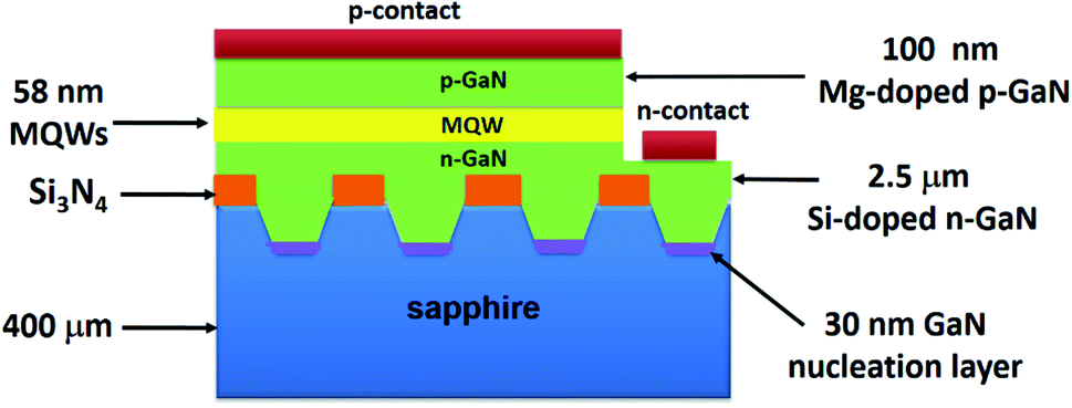 | ||
| Fig. 1 The schematic diagram of PSS-LED with Si3N4 layer. | ||
These samples were characterized by scanning electron microscopy (SEM) and transmission electron microscopy (TEM) to reveal the surface morphology and cross-sectional structure. The temperature-dependent photoluminescence (PL) was employed for evaluation of the internal quantum efficiency. Finally, we performed optical simulation by TracePro to investigate the luminous efficiency of LED. We build four structures and namely, conventional LED (C-LED), patterned sapphire substrate LED (PSS-LED), patterned sapphire substrate LED with Si3N4 barrier (PSN-LED), and patterned sapphire substrate LED with SiO2 barrier (PSO-LED).
3. Results and discussion
In order to confirm the experiment feasibility, we performed optical simulation before the experiment. Fig. 2 shows the simulation result of PSN-LED and PSO-LED. It reveals that both LEDs, especially PSN-LED, have higher luminous efficiency than PSS-LED. The reason is that by using Si3N4 as the gradient refractive index material, the luminous efficiency of PSN-LED will be enhanced by 62.7% compared with that of PSS-LED. The simulation result also shows that the luminous efficiency of PSN-LED can be significantly improved when the interlayer thickness ranges from 110 to 440 nm. It indicated that the suitable thickness in simulation is the range of 110–440 nm (the sample with different thicknesses, 110 nm, 220 nm, 330 nm and 440 nm is named as sample A, sample B, sample C, and sample D.) | ||
| Fig. 2 The simulation results of PSN-LED and PSO-LED. | ||
Fig. 3 shows the top view, 30-degree tilt, and cross-sectional SEM images of PSN-LEDs. The pyramidal patterned was formed after wet etching at 260 °C for 4.5 min by H2SO4:H3PO4 = 5:1 mixture solution. The depth of each pyramidal pattern is 371 nm approximately. In addition, we not only successfully etched a perfect patterned sapphire substrate but also kept a textured Si3N4 film on top of the patterns. Before the patterned sapphire substrate was fabricated, the Si3N4 pattern was treated by dry etching with CHF3 and Ar gases. After dry etching, the surface of Si3N4 intermediate layer was textured due to the plasma damage, which will induce the generation of air voids after lateral growth of GaN, so called PSA-LED.
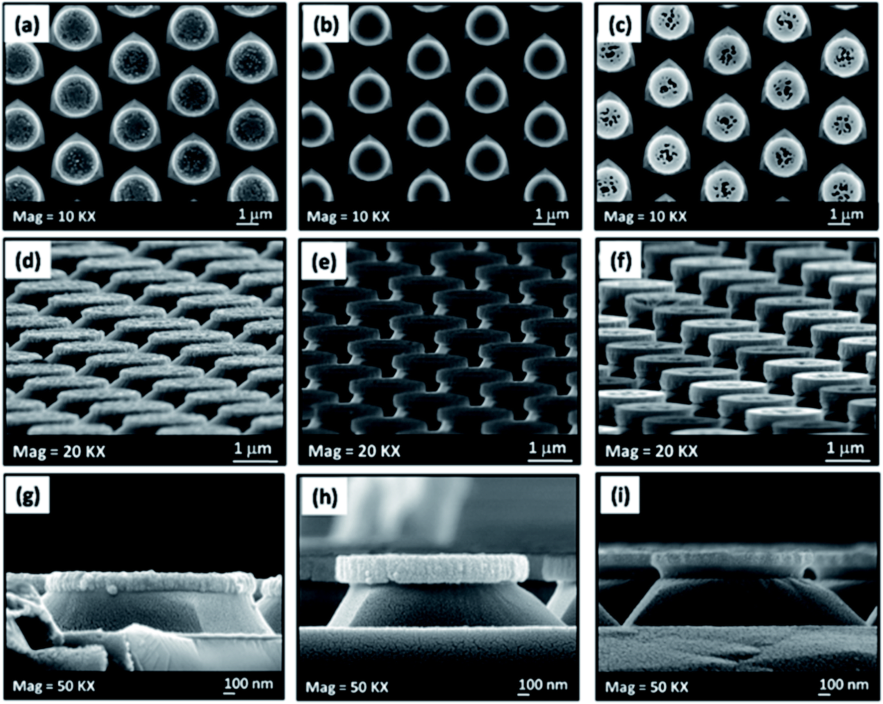 | ||
| Fig. 3 The SEM images of patterned sapphire substrate etched at 260 °C and 4.5 min: (a)–(c) top view SEM images of 110, 220, 330 nm; (d)–(f) tilted view and (g)–(i) cross-sectional SEM images of 110, 220, 330 nm. | ||
Fig. 4(a) shows the LIV results of the fabricated PSA-LEDs. The light output power of sample B has the maximum value, 5 mW, at 350 mA injection current. It is approximately 40% higher than that of the PSS-LED, which is the commercial PSS-LED with SiO2 intermediate layer. Accordingly, significantly increased luminous efficiency for high power PSA-LED chip can be achieved by employing Si3N4. Fig. 4(b) shows the measured wavelength of PSA-LED with different thickness. The intensity of PSA-LED with 220 nm-thick Si3N4 is 40% higher than that of PSS-LED at 450 nm.
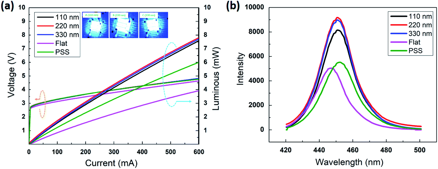 | ||
| Fig. 4 (a) The LIV results of PSA-LEDs and (b) the wavelength of PSA-LEDs. | ||
Fig. 5 shows the TEM images of GaN grown on the PSS. The unexpected air void was observed on top of the textured Si3N4 intermediate layer in Fig. 5(a). The threading dislocations propagating through the whole GaN layer from the sapphire. Conversely, there is dislocation-free region on top of the textured Si3N4 intermediate layer. Only one threading dislocation was generated when the GaN laterally coalesced on top of pattern in Fig. 5(d) and (e). Besides, the stacking faults were formed in the GaN epilayer as shown in Fig. 5(f). These stacking faults interact with the vertical threading dislocations and bend them horizontally. These pieces of evidence all indicated that the presence of PSS induced the subsequent epitaxial layer lateral growth, thus yielding the presence of air voids. Thus, the PSS LED with Si3N4 embedded air void was called as PSA-LED.
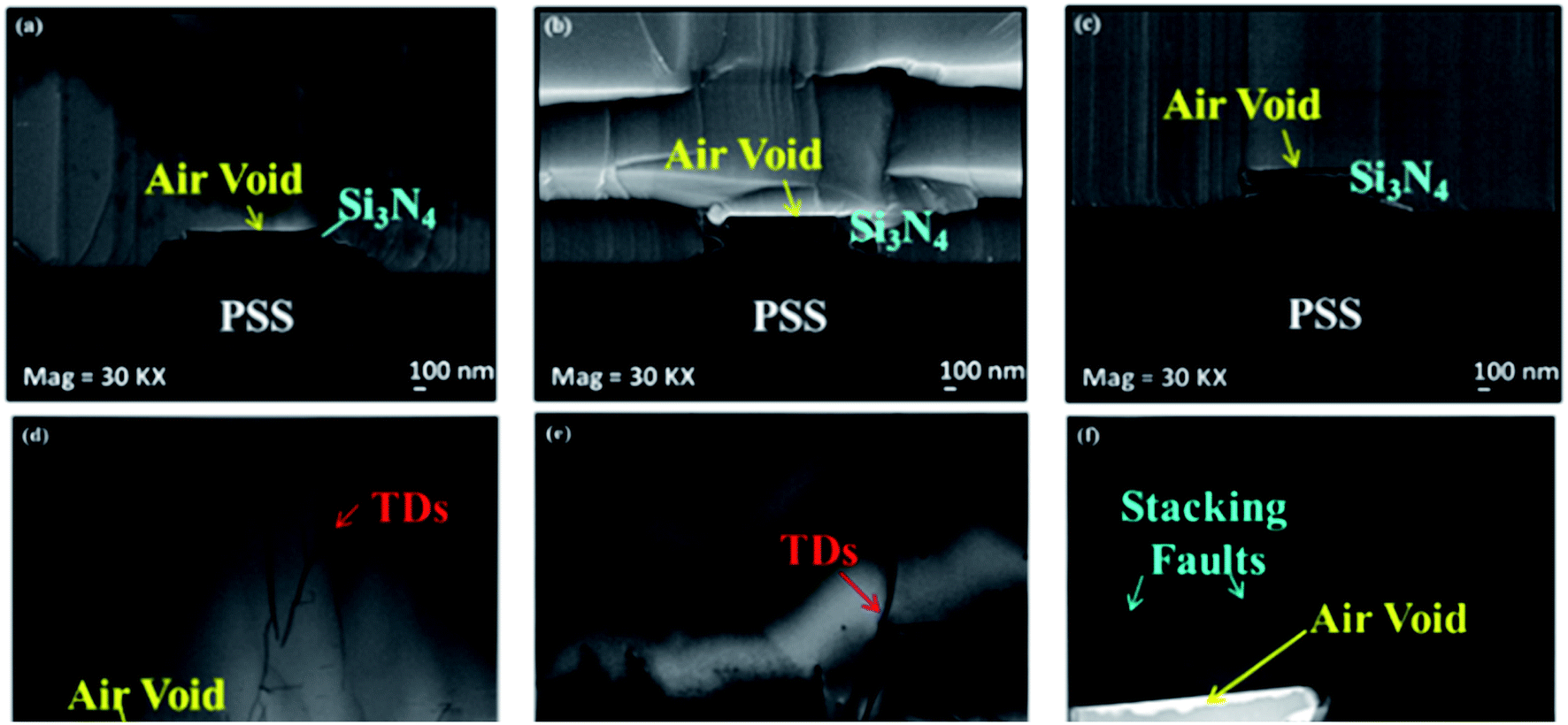 | ||
| Fig. 5 The TEM images of GaN grown on the patterned sapphire substrate: (a)–(c) air voids exist onto the Si3N4 layer; (d)–(f) the distribution of threading dislocations and stacking faults in the GaN epilayer. | ||
In order to confirm the GaN crystalline quality, the temperature-dependent PL was used to estimate the IQE of the LED devices. Fig. 6 shows the PL results for PSS-LEDs and PSA-LEDs with Si3N4 of 110 nm, 220 nm, and 330 nm thickness. The IQE values at room temperature are 8.87%, 12.77%, 40.48% and 11.29%, respectively. The PSA-LED with 220 nm Si3N4 has the highest IQE value, which is 4.56 times the IQE value of the PSS-LED at room temperature. This indicates that crystalline quality can be improved by applying the formation of air voids.
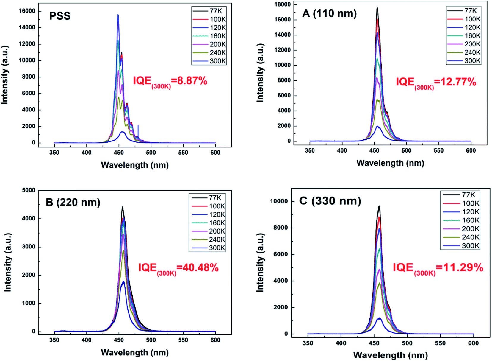 | ||
| Fig. 6 Temperature-dependent PL results of PSS-LED and PSA-LEDs. | ||
Furthermore, optical simulation was performed to verify whether the air voids exist in the GaN epi-layer affect the luminous efficiency of LED or not. Fig. 7 shows the simulation results of four different structures, namely PSS-LED, PSN-LED, PSA-LED and PSO-LED. The results display that the air voids indeed affect the final luminous efficiency. The luminous efficiency rank of the four different LEDs is PSN-LED > PSA-LED > PSO-LED > PSS-LED.
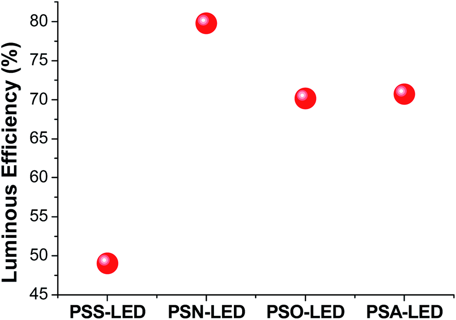 | ||
| Fig. 7 The simulation results of PSS-LED, PSN-LED, PSA-LED and PSO-LED. | ||
In terms of Snell's Law, larger critical angle induces higher LEE. The critical angle of GaN and sapphire is 47.87°. In the case of planar sapphire substrate, most light emerge total internal reflection when the incident angle becomes larger than the critical angle of 47.87° (dash line a, b, c) as shown in Fig. 8(a). If the patterned sapphire substrate instead of the planar sapphire substrate, the light will emit downward to sapphire because the sidewall of patterns reduces the incident angle. That's why using patterned sapphire substrate can enhance LEE (Fig. 8(b) the light ray B1). Fig. 8(c) shows a LED structure inserts an interlayer on top of patterned sapphire in which refractive index falls between GaN and sapphire. In other words, the interlayer can be used as a gradient refractive index material. The light can be extracted downward to the sapphire easily because the critical angle becomes larger (the light ray C1). In other words, the technique reduces the total internal reflection effectively. Conversely, if the interlayer's refractive index is smaller than that of the sapphire, the total internal reflection become further enhanced. Original light D will be smoothly escape to the outside, but the critical angle becomes smaller than 47.87° so that the light is reflected to inner of LED. According to the Snell's law, the bigger difference of refractive index, the more total internal reflection is made.
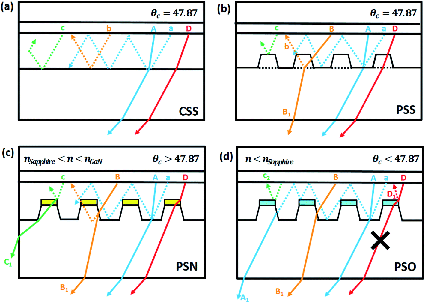 | ||
| Fig. 8 The light rays for four structures of LED (a) C-LED (b) PSS-LED (c) the refractive index between that of GaN and sapphire (d) the refractive index smaller than that of sapphire. | ||
From the light point distribution analysis, the different light point position obtains different LEE as shown in Fig. 9. By three light point positions simulation, namely, between the PSS (BETWEEN), center of the PSS (CENTER), and edge of the top of PSS (EDGE). In terms of PSS-LED with PSO-LED, when the light point is set on the CENTER position, the PSS-LED produces higher luminous efficiency than PSO-LED. Nevertheless, when the light point is set on the BETWEEN position and EDGE position, the PSO-LED has at least one-time higher luminous efficiency than PSO-LED. And, the PSA-LED has nearly the same condition as PSO-LED. That's why the PSA-LED and PSO-LED's luminous efficiency are superior than that of PSS-LED in spite of the fact that their refractive index values are both smaller than the sapphire. The simulation results show that the PSN-LED has the best luminous efficiency because of its incorporation of gradient refractive index material.
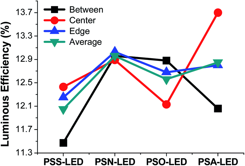 | ||
| Fig. 9 The simulation results for three different light point positions. | ||
4. Conclusions
In this study, the optical properties of patterned sapphire substrate were investigated and reported. The threading dislocations were reduced because the subsequent epitaxial growth is similar to the mechanism of ELOG. Moreover, since the textured Si3N4 surface was retained on top of the patterns, it made the formation of air voids after GaN laterally growth process. The simulation results revealed that the PSN-LED showed the best luminous efficiency because the Si3N4 served as the gradient refractive index layer. The LEE was approximately 62.7% higher than that of the conventional PSS-LED. In the experiment, the LED structure with Si3N4 intermediate layer of 220 nm thickness had the best lighting performance. The luminous intensity and IQE of PSA-LED with 220 nm-thick Si3N4 is 40% and 4.56 times higher than that of PSS-LED at 450 nm.Conflicts of interest
There are no conflicts to declare.Acknowledgements
This work was financially supported by the Ministry of Science and Technology (MOST) of the Republic of China (Taiwan) under Grants 105-2221-E-032-058 and 107-2221-E-032-034. L. H. Y. acknowledges the funding supported by MOST under the Shackleton Program award No. 108-2638-E-002-003-MY2.References
- T. Ayari, S. Sundaram, C. Bishop, A. Mballo, P. Vuong, Y. Halfaya, S. Karrakchou, S. Gautier, P. L. Voss and J. P. Salvestrini, Adv. Mater. Technol., 2019, 4, 1900164 CrossRef CAS.
- Z. Chen, J. Hoo, Y. Chen, V. Wang and S. Guo, Jpn. J. Appl. Phys., 2019, 58, SC1007 CrossRef CAS.
- C. Chiu, Z.-Y. Li, C. Chao, M. Lo, H. Kuo, P. Yu, T. Lu, S. Wang, K. Lau and S. Cheng, J. Cryst. Growth, 2008, 310, 5170–5174 CrossRef CAS.
- H. K. Cho, J. Y. Lee, K. S. Kim, G. M. Yang, J. H. Song and P. W. Yu, J. Appl. Phys., 2001, 89, 2617–2621 CrossRef CAS.
- J.-Y. Cho, J.-S. Kim, Y.-D. Kim, H. J. Cha and H. Lee, Jpn. J. Appl. Phys., 2015, 54, 02BA04 CrossRef.
- M. Chugh and M. Ranganathan, Phys. Chem. Chem. Phys., 2017, 19, 2111–2123 RSC.
- T. Cuong, H. Cheong, H. Kim, H. Kim, C.-H. Hong, E. Suh, H. Cho and B. Kong, Appl. Phys. Lett., 2007, 90, 131107 CrossRef.
- N. P. Gaponik, D. V. Talapin and A. L. Rogach, Phys. Chem. Chem. Phys., 1999, 1, 1787–1789 RSC.
- M. Han, N. Han, E. Jung, B. D. Ryu, K. B. Ko, T. viet Cuong, H. Kim, J. K. Kim and C.-H. Hong, Semicond. Sci. Technol., 2016, 31, 085010 CrossRef.
- E.-J. Hong, K.-J. Byeon, H. Park, J. Hwang, H. Lee, K. Choi and H.-S. Kim, Solid-State Electron., 2009, 53, 1099–1102 CrossRef CAS.
- K.-C. Huang, Y.-R. Huang, C.-M. Tseng, S. H. Tseng and J.-E. Huang, Scr. Mater., 2015, 108, 40–43 CrossRef CAS.
- S. Huang, C. Chang, H. Lin, X. Li, Y. Lin and C. Liu, Thin Solid Films, 2017, 628, 127–131 CrossRef CAS.
- S.-M. Jeong, S. Kissinger, D.-W. Kim, S. J. Lee, J.-S. Kim, H.-K. Ahn and C.-R. Lee, J. Cryst. Growth, 2010, 312, 258–262 CrossRef CAS.
- A. Jiménez-Solano, L. Martínez-Sarti, A. Pertegás, G. Lozano, H. J. Bolink and H. Míguez, Phys. Chem. Chem. Phys., 2020, 22, 92–96 RSC.
- F.-I. Lai, Y.-L. Hsieh and W.-T. Lin, Diamond Relat. Mater., 2011, 20, 770–773 CrossRef CAS.
- D. Lee, J. W. Lee, J. Jang, I.-S. Shin, L. Jin, J. H. Park, J. Kim, J. Lee, H.-S. Noh and Y.-I. Kim, Appl. Phys. Lett., 2017, 110, 191103 CrossRef.
- Y.-J. Moon, D. Moon, J. Jang, J.-Y. Na, J.-H. Song, M.-K. Seo, S. Kim, D. Bae, E. H. Park and Y. Park, Nano Lett., 2016, 16, 3301–3308 CrossRef CAS PubMed.
- S. Zhou, H. Xu, H. Hu, C. Gui and S. Liu, Appl. Surf. Sci., 2019, 471, 231–238 CrossRef CAS.
- H. Hu, B. Tang, H. Wan, H. Sun, S. Zhou, J. Dai, C. Chen, S. Liu and L. J. Guo, Nano Energy, 2020, 69, 104427 CrossRef.
- S. Zhou, X. Liu, H. Yan, Z. Chen, Y. Liu and S. Liu, Opt. Express, 2019, 27, A669–A692 CrossRef CAS PubMed.
- S. Zhou, X. Liu, Y. Gao, Y. Liu, M. Liu, Z. Liu, C. Gui and S. Liu, Opt. Express, 2017, 25, 26615–26627 CrossRef CAS PubMed.
- G. S. Lee, C. Lee, H. Jeon, C. Lee, S. G. Bae, H. S. Ahn, M. Yang, S. N. Yi, Y. M. Yu and J. H. Lee, Jpn. J. Appl. Phys., 2016, 55, 05FC02 CrossRef.
- Y.-J. Lee, H.-C. Kuo, T.-C. Lu and S.-C. Wang, IEEE J. Quantum Electron., 2006, 42, 1196–1201 CAS.
- H. Hu, S. Zhou, X. Liu, Y. Gao, C. Gui and S. Liu, Sci. Rep., 2017, 7, 1–10 Search PubMed.
- S. Zhou, H. Hu, X. Liu, M. Liu, X. Ding, C. Gui, S. Liu and L. J. Guo, Jpn. J. Appl. Phys., 2017, 56, 111001 CrossRef.
- Z. Lin, H. Wang, W. Wang, Y. Lin, M. Yang, S. Chen and G. Li, Opt. Express, 2016, 24, 11885–11896 CrossRef CAS PubMed.
- Y. H. Sung, J. Park, E.-S. Choi, H. C. Lee and H. Lee, Sci. Adv. Mater., 2020, 12, 647–651 CrossRef.
- Y.-J. Lee, C.-J. Lee and C.-H. Chen, IEEE J. Quantum Electron., 2011, 47, 636–641 CAS.
- B.-W. Lin, C.-Y. Hsieh, B.-M. Wang, W.-C. Hsu and Y. S. Wu, Electrochem. Solid-State Lett., 2011, 14, J48–J50 CrossRef CAS.
- S. Zhou, Z. Lin, H. Wang, T. Qiao, L. Zhong, Y. Lin, W. Wang, W. Yang and G. Li, J. Alloys Compd., 2014, 610, 498–505 CrossRef CAS.
- I. H. Malitson, J. Opt. Soc. Am., 1962, 52, 1377–1379 CrossRef CAS.
- M. Mishra, A. Gundimeda, S. Krishna, N. Aggarwal, B. Gahtori, N. Dilawar, V. V. Aggarwal, M. Singh, R. Rakshit and G. Gupta, Phys. Chem. Chem. Phys., 2017, 19, 8787–8801 RSC.
- O.-H. Nam, T. S. Zheleva, M. D. Bremser and R. F. Davis, J. Electron. Mater., 1998, 27, 233–237 CrossRef CAS.
- Q. Nie, Z. Jiang, Z. Gan, S. Liu, H. Yan and H. Fang, J. Cryst. Growth, 2018, 488, 1–7 CrossRef CAS.
- W.-h. Sang, L. Lin, L. Wang, J.-h. Min, J.-j. Zhu and M.-r. Wang, Optoelectron. Lett., 2016, 12, 178–181 CrossRef.
- Y.-K. Su, P.-C. Wang, C.-L. Lin, G.-S. Huang and C.-M. Wei, IEEE Electron Device Lett., 2014, 35, 575–577 CAS.
- P. Törmä, O. Svensk, M. Ali, S. Suihkonen, M. Sopanen, M. Odnoblyudov and V. Bougrov, Solid-State Electron., 2009, 53, 166–169 CrossRef.
- B. T. Tran, N. Maeda, M. Jo, D. Inoue, T. Kikitsu and H. Hirayama, Sci. Rep., 2016, 6, 35681 CrossRef CAS.
- D.-H. Wang, T.-H. Xu and L. Wang, Curr. Opt. Photonics, 2017, 1, 358–363 CAS.
- H. Wang, X. Wang, Q. Tan and X. Zeng, Mater. Sci. Semicond. Process., 2015, 29, 112–116 CrossRef CAS.
- D.-S. Wuu, H.-W. Wu, S.-T. Chen, T.-Y. Tsai, X. Zheng and R.-H. Horng, J. Cryst. Growth, 2009, 311, 3063–3066 CrossRef CAS.
- Y. Xu, J. Zou, X. Lin, W. Wu, W. Li, B. Yang and M. Shi, Appl. Sci., 2018, 8, 1842 CrossRef.
- M. Yamada, T. Mitani, Y. Narukawa, S. Shioji, I. Niki, S. Sonobe, K. Deguchi, M. Sano and T. Mukai, Jpn. J. Appl. Phys., Part 1, 2002, 41, L1431 CrossRef CAS.
- Y. J. Yun, J. K. Kim, J. Y. Ju, S. K. Choi, W. I. Park, J. Y. Suh, H.-k. Jung, Y. Kim and S. Choi, Phys. Chem. Chem. Phys., 2017, 19, 11111–11119 RSC.
- T. S. Zheleva, O.-H. Nam, M. D. Bremser and R. F. Davis, Appl. Phys. Lett., 1997, 71, 2472–2474 CrossRef CAS.
- Q. Zhou, M. Xu, Q. Li and H. Wang, IEEE Photonics Technol. Lett., 2017, 29, 983–986 CAS.
- S. Zhou, S. Yuan, Y. Liu, L. J. Guo, S. Liu and H. Ding, Appl. Surf. Sci., 2015, 355, 1013–1019 CrossRef CAS.
Footnote |
| † These two authors contributed equally to this work. |
| This journal is © The Royal Society of Chemistry 2020 |